Note: Descriptions are shown in the official language in which they were submitted.
CA 02437874 2003-08-08
WO 02/065077 PCT/US02/03283
TEMPERATURE-SENSING COMPOSITION
FEDERALLY SPONSORED RESEARCH OR DEVELOPMENT
This invention was made with government support under Contract No. DMR-98-
08941 from the National Science Foundation and Subcontract No. 301251 from
Contract
No. F33615-98-C-3012 from Air Force Office of Sponsored Research. The
government
may have certain rights in the invention.
TECHNICAL FIELD
This invention relates to a temperature-sensing composition.
BACKGROUND
Specialty compositions, which can contain luminescent probes that are
sensitive to
environmental parameters such as, for example, temperature and pressure, have
a variety
of analytical applications. For example, specialty compositions can form
coatings used to
remotely determine the surface temperature of an object in a non-invasive
manner.
Objects can be coated with films containing the sensing compositions which
emit
light of varying intensities, depending on temperature and oxygen pressure. In
a specific
example, temperature-sensing compositions can be used in combination with
compositions for measuring the pressure of an oxygen-containing gas on an
aerodynamic
surface by oxygen-quenching of luminescent pressure sensing compositions.
These
compositions can be used to provide convenient and inexpensive methods for
determining
pressure or temperature maps at surfaces. An example of a pressure-sensing
composition
2o includes a phosphorescent porphyrin which has an emission that is quenched
by oxygen.
This quenching can be used to quantitatively measure the static pressure on
the surface of
the object. In certain circumstances, the emission of the pressure-sensing
composition
can have temperature dependence in addition to pressure dependence.
Accordingly,
pressure measurements containing a temperature-sensing composition can be
corrected by
25 sensing fluctuations in the temperature in addition to pressure.
SUMMARY
Temperature-sensing compositions can include an inorganic material, such as a
semiconductor nanocrystal. The nanocrystal can be a dependable and accurate
indicator
of temperature. The intensity of emission of the nanocrystal varies with
temperature and
3o can be highly sensitive to surface temperature. The nanocrystals can be
processed with a
-I-
CA 02437874 2003-08-08
WO 02/065077 PCT/US02/03283
binder to form a matrix, which can be varied by altering the chemical nature
of the
surface of the nanocrystal. A nanocrystal with a compatibilizing outer layer
can be
incorporated into a coating formulation and retain its temperature sensitive
emissive
properties.
In one aspect, a method of sensing temperature includes providing a
temperature
sensor including a matrix on a surface of a substrate, the matrix comprising a
semiconductor nanocrystal in a binder, irradiating a portion of the sensor
with an
excitation wavelength of light, detecting emission of light from the sensor,
and
determining the temperature from the emission of light from the sensor.
o In another aspect, a temperature sensor includes a matrix containing a
semiconductor nanocrystal. The matrix can be formed from a semiconductor
nanocrystal
and a binder.
In another aspect, a temperature-sensing coating includes a matrix on a
surface of
a substrate. The matrix can include a semiconductor nanocrystal in a binder.
~ 5 In another aspect, a temperature-sensing paint includes a semiconductor
nanocrystal in a binder and a deposition solvent. The semiconductor
nanocrystal can emit
light independent of oxygen pressure and dependent upon temperature upon
irradiation by
an excitation wavelength of light. The emission intensity can change by 1. l-
1.6% per
degree centigrade. The paint can include a pressure-sensitive composition, the
pressure-
2o sensitive composition emitting light dependent upon oxygen pressure upon
irradiation by
an excitation wavelength of light. The pressure-sensitive composition can
include a
porphyrin, such as a platinum porphyrin. The deposition solvent can include an
alcohol.
In another aspect, a method of manufacturing a temperature-sensing paint
includes
combining a semiconductor nanocrystal, a binder, and a deposition solvent to
form a
25 paint. The paint can be used to manufacture a temperature sensor by
depositing a
temperature-sensing paint on a surface of a substrate.
The semiconductor nanocrystal can include a group II-VI semiconductor, a group
III-V semiconductor, or group IV semiconductor, for example, ZnS, ZnSe, ZnTe,
CdS,
CdSe, CdTe, HgS, HgSe, HgTe, A1N, A1P, AIAs, AISb, GaN, GaP, GaAs, GaSb, InN,
InP,
3o InAs, InSb, T1N, T1P, TIAs, TISb, PbS, PbSe, PbTe, or mixtures thereof. The
semiconductor nanocrystal can be overcoated with a second semiconductor
material. The
semiconductor nanocrystal can include an organic or organometallic overlayer,
the
overlayer making the nanocrystal dispersible in the binder. The overlayer can
include a.
hydrolyzable moiety, such as a metal alkoxide.
-2-
CA 02437874 2003-08-08
WO 02/065077 PCT/US02/03283
The nanocrystal can be a member of a substantially monodisperse core
population,
such as a population exhibiting less than a 15% tins deviation in diameter of
the
nanocrystal, which can emit light in a spectral range of no greater than about
75 nm full
width at half max (FWHM). The nanocrystal can photoluminesce with a quantum
efficiency of at least 10% and can have a particle size in the range of about
15 ~ to about
125 ~.
The binder can include an organic polymer or inorganic matrix.
The details of one or more embodiments are set forth in the accompanying
drawings and the description below. Other features and advantages will be
apparent from
the description and drawings, and from the claims.
DESCRIPTION OF DRAWINGS
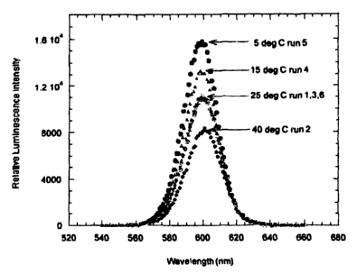
Figure 1 is a graph depicting emission spectra of ZnS-capped CdSe nanocrystals
in a poly(lauryl methacrylate) matrix irradiated at 480 nm at various
temperatures.
Figure 2 is a graph depicting integrated emission intensity of the ZnS-capped
~5 CdSe nanocrystals dispersed in a matrix over a range of temperatures.
DETAILED DESCRIPTION
A temperature-sensing composition can include a semiconductor nanocrystal.
Nanocrystals composed of semiconductor material can be illuminated with a
light source
at an absorption wavelength to cause an emission at an emission wavelength,
the emission
2o having a frequency that corresponds to the band gap of the quantum confined
semiconductor material. The band gap is a function of the size of the
nanocrystal.
Nanocrystals having small diameters can have properties intermediate between
molecular
and bulk forms of matter. For example, nanocrystals based on semiconductor
materials
having small diameters can exhibit quantum confinement of both the electron
and hole in
25 all three dimensions, which leads to an increase in the effective band gap
of the material
with decreasing crystallite size. Consequently, both the optical absorption
and emission
of nanocrystals shift to the blue (i.e., to higher energies) as the size of
the crystallites
decreases.
The emission from the nanocrystal can be a narrow Gaussian emission band that
3o can be tuned through the complete wavelength range of the ultraviolet,
visible, or infrared
regions of the spectrum by varying the size of the nanocrystal, the
composition of the
nanocrystal, or both. For example, CdSe can be tuned in the visible region and
InAs can
-3-
CA 02437874 2003-08-08
WO 02/065077 PCT/US02/03283
be tuned in the infrared region. The narrow size distribution of a population
of
nanocrystals can result in emission of light in a narrow spectral range. The
population
can exhibit less than a 15% rms deviation in diameter of the nanocrystals,
preferably less
than 10%, more preferably less than 5%. Spectral emissions in a narrow range
of no
greater than about 75 nm, preferably 60 nm, more preferably 40 nm, and most
preferably
30 nm full width at half max (FWHM) can be observed. The breadth of the
emission
decreases as the dispersity of nanocrystal diameters decreases. Semiconductor
nanocrystals can have high emission quantum efficiencies such as greater than
10%, 20%,
30%, 40%, 50%, 60%, 70%, or 80%.
o The narrow emission band of the nanocrystal can improve the performance and
reliability of the temperature-sensing composition relative to compositions
that include
conventional molecular probes that have broad, fixed wavelength emission
bands. In
addition, the excitation profile of the nanocrystal can be broad and intense,
which can
allow efficient excitation of the nanocrystals across a range of wavelengths
in the visible
~ 5 spectrum. These factors together offer flexibility in the design of
optical detection
systems for temperature-sensing applications.
The nanocrystal can be chemically stable when illuminated. The nanocrystal can
be relatively unreactive with other materials, which can permit it to be used
as a
temperature probe in a wide variety of environments. For example, the emission
of the
2o nanocrystal can be independent of gas pressure, such as oxygen pressure, or
resistant to
degradation in the presence of oxygen. Conventional organic temperature probes
can
degrade rapidly when illuminated, decreasing the useful lifespan of the
coatings that
contain them. A variety of applications can be envisioned for temperature-
sensing
compositions that contain nanocrystals on the well-defined temperature
dependent
25 emission properties of the nanocrystal. For example, in aerospace
engineering,
nanocrystal-based temperature indicators can be used as the active component
in
temperature sensitive paints or as an internal temperature calibrant for two-
component
pressure sensitive paints.
Methods of preparing monodisperse semiconductor nanocrystals include pyrolysis
30 of organometallic reagents, such as dimethyl cadmium, injected into a hot,
coordinating
solvent. This permits discrete nucleation and results in the controlled growth
of
macroscopic quantities of nanocrystals. Preparation and manipulation of
nanocrystals are
described, for example, in U.S. Appln. No. 08/969,302, incorporated herein by
reference
in its entirety. The method of manufacturing a nanocrystal is a colloidal
growth process.
-4-
CA 02437874 2003-08-08
WO 02/065077 PCT/US02/03283
Colloidal growth occurs by rapidly injecting an M donor and an X donor into a
hot
coordinating solvent. The injection produces a nucleus that can be grown in a
controlled
manner to form a nanocrystal. The reaction mixture can be gently heated to
grow and
anneal the nanocrystal. Both the average size and the size distribution of the
nanocrystals
in a sample are dependent on the growth temperature. The growth temperature
necessary
to maintain steady growth increases with increasing average crystal size. The
nanocrystal
is a member of a population of nanocrystals. As a result of the discrete
nucleation and
controlled growth, the population of nanocrystals obtained has a narrow,
monodisperse
distribution of diameters. The monodisperse distribution of diameters can also
be referred
to as a size. The process of controlled growth and annealing of the
nanocrystals in the
coordinating solvent that follows nucleation can also result in uniform
surface
derivatization and regular core structures. As the size distribution sharpens,
the
temperature can be raised to maintain steady growth. By adding more M donor or
X
donor, the growth period can be shortened.
~ 5 The M donor can be an inorganic compound, an organometallic compound, or
elemental metal. M is cadmium, zinc, magnesium, mercury, aluminum, gallium,
indium
or thallium. The X donor is a compound capable of reacting with the M donor to
form a
material with the general formula MX. Typically, the X donor is a chalcogenide
donor or
a pnictide donor, such as a phosphine chalcogenide, a bis(silyl) chalcogenide,
dioxygen,
2o an ammonium salt, or a tris(silyl) pnictide. Suitable X donors include
dioxygen,
bis(trimethylsilyl) selenide ((TMS)ZSe), trialkyl phosphine selenides such as
(tri-n-
octylphosphine) selenide (TOPSe) or (tri-n-butylphosphine) selenide (TBPSe),
trialkyl
phosphine tellurides such as (tri-n-octylphosphine) telluride (TOPTe) or
hexapropylphosphorustriamide telluride (HPPTTe), bis(trimethylsilyl)telluride
25 ((TMS)zTe), bis(trimethylsilyl)sulfide ((TMS)ZS), a trialkyl phosphine
sulfide such as (tri-
n-octylphosphine) sulfide (TOPS), an ammonium salt such as an ammonium halide
(e.g.,
NH4Cl), tris(trimethylsilyl) phosphide ((TMS)3P), tris(trimethylsilyl)
arsenide
((TMS)3As), or tris(trimethylsilyl) antimonide ((TMS)3Sb). In certain
embodiments, the
M donor and the X donor can be moieties within the same molecule.
3o A coordinating solvent can help control the growth of the nanocrystal. The
coordinating solvent is a compound having a donor lone pair that, for example,
has a lone
electron pair available to coordinate to a surface of the growing nanocrystal.
Solvent
coordination can stabilize the growing nanocrystal. Typical coordinating
solvents include
alkyl phosphines, alkyl phosphine oxides, alkyl phosphonic acids, or alkyl
phosphinic
-5-
CA 02437874 2003-08-08
WO 02/065077 PCT/US02/03283
acids, however, other coordinating solvents, such as pyridines, furans, and
amines may
also be suitable for the nanocrystal production. Examples of suitable
coordinating
solvents include tri-n-octyl phosphine (TOP) and tri-n-octyl phosphine oxide
(TOPO).
Technical grade TOPO can be used.
Size distribution during the growth stage of the reaction can be estimated by
monitoring the absorption line widths of the particles. Modification of the
reaction
temperature in response to changes in the absorption spectrum of the particles
allows the
maintenance of a sharp particle size distribution during growth. Reactants can
be added
to the nucleation solution during crystal growth to grow larger crystals. By
stopping
growth at a particular nanocrystal average diameter and choosing the proper
composition
of the semiconducting material, the emission spectra of the nanocrystals can
be tuned
continuously over the wavelength range of 400 nm to 800 nm. The nanocrystal
has a
diameter of less than 150 ~. A population of nanocrystals has average
diameters in the
range of 1 S ~ to 125 ~.
The nanocrystal can be a member of a population of nanocrystals having a
narrow
size distribution. The nanocrystal can be a sphere, rod, disk, or other shape.
The
nanocrystal can include a core of a semiconductor material. The nanocrystal
can include
a core having the formula MX, where M is cadmium, zinc, magnesmm, mercury,
aluminum, gallium, indium, thallium, or mixtures thereof, and X is oxygen,
sulfur,
2o selenium, tellurium, nitrogen, phosphorus, arsenic, antimony, or mixtures
thereof.
The core can have an overcoating on a surface of the core. The overcoating can
be a semiconductor material having a composition different from the
composition of the
core. The overcoat of a semiconductor material on a surface of the nanocrystal
can
include a group II-VI, III-V or IV semiconductor, such as, for example, ZnO,
ZnS, ZnSe,
25 ZnTe, CdO, CdS, CdSe, CdTe, MgO, MgS, MgSe, MgTe, HgO, HgS, HgSe, HgTe,
AIN,
A1P, AIAs, AISb, GaN, GaP, GaAs, GaSb, InN, InP, InAs, InSb, T1N, T1P, TIAs,
TISb,
TISb, PbS, PbSe, PbTe, or mixtures thereof. For example, ZnS, ZnSe or CdS
overcoatings
can be grown on CdSe or CdTe nanocrystals. An overcoating process is
described, for
example, in U.S. Application No. 08/969,302, incorporated herein by reference
in its
so entirety. By adjusting the temperature of the reaction mixture during
overcoating and
monitoring the absorption spectrum of the core, over coated materials having
high
emission quantum efficiencies and narrow size distributions can be obtained.
The particle size distribution can be further refined by size selective
precipitation
with a poor solvent for the nanocrystals, such as methanol/butanol as
described in U.S.
-6-
CA 02437874 2003-08-08
WO 02/065077 PCT/US02/03283
Application No. 08/969,302, incorporated herein by reference. For example,
nanocrystals
can be dispersed in a solution of 10% butanol in hexane. Methanol can be added
dropwise to this stirring solution until opalescence persists. Separation of
supernatant and
flocculate by centrifugation produces a precipitate enriched with the largest
crystallites in
the sample. This procedure can be repeated until no further sharpening of the
optical
absorption spectrum is noted. Size-selective precipitation can be carried out
in a variety
of solvent/nonsolvent pairs, including pyridine/hexane and
chloroform/methanol. The
size-selected nanocrystal population can have no more than a 15% RMS deviation
from
mean diameter, preferably 10% RMS deviation or less, and more preferably 5%
RMS
deviation or less.
Transmission electron microscopy (TEM) can provide information about the size,
shape, and distribution of the nanocrystal population. Powder x-ray
diffraction (XRD)
patterns can provided the most complete information regarding the type and
quality of the
crystal structure of the nanocrystals. Estimates of size are also possible
since particle
15 diameter is inversely related, via the X-ray coherence length, to the peak
width. For
example, the diameter of the nanocrystal can be measured directly by
transmission
electron microscopy or estimated from x-ray diffraction data using, for
example, the
Schemer equation. It also can be estimated from the UV/Vis absorption
spectrum.
The outer surface of the nanocrystal can include layer of compounds derived
from
2o the coordinating solvent used during the growth process. The surface can be
modified by
repeated exposure to an excess of a competing coordinating group to fomn an
overlayer.
For example, a dispersion of the capped nanocrystal can be treated with a
coordinating
organic compound, such as pyridine, to produce crystallites which disperse
readily in
pyridine, methanol, and aromatics but no longer disperse in aliphatic
solvents. Such a
25 surface exchange process can be carried out with any compound capable of
coordinating
to or bonding with the outer surface of the nanocrystal, including, for
example,
phosphines, thiols, amines and phosphates. The nanocrystal can be exposed to
short
chain polymers which exhibit an affinity for the surface and which terminate
in a moiety
having an affinity for a suspension or dispersion medium. Such affinity
improves the
3o stability of the suspension and discourages flocculation of the
nanocrystal.
The compound forming the overlayer can have a reactive group that can react
with
another compound to bond the nanocrystal to the binder. The binder can form a
matrix.
The matrix can be an organic polymer matrix, such as a polyacrylate matrix, or
an
inorganic matrix, such as a sol-gel-derived matrix.
_7-
CA 02437874 2003-08-08
WO 02/065077 PCT/US02/03283
The reactive group can be a polymerizable moiety, such as an acrylate moiety,
a
stryryl moiety, or a hydrolyzable moiety, for example, silicon alkoxide,
titanium alkoxide,
zirconium alkoxide, or other metal alkoxide, metal amide, metal carboxylate,
or metal
halide groups. The reactive groups can react with each other, or with reactive
groups of
other compounds or monomers, to form a solid matrix containing the
nanocrystals. In
this manner, the nanocrystal can be incorporated into a solid matrix formed in
part by
reaction of the reactive groups. Alternatively, the reactive group can be a
functionality,
such as an amino or hydroxyl group, that can react with a multifunctional
component,
such as a dicarboxylic acid, or reactive derivative thereof, or a
diisocyanate, to form a
o solid matrix containing the nanocrystals.
The temperature-sensing composition can be applied to a substrate as a paint.
The
paint can include a binder and a deposition solvent. The binder can produce a
film on a
surface of an object upon evaporation of solvent. The binder can include an
organic or
inorganic polymer or prepolymer, for example, a polymer or prepolymer
typically used in
~5 a paint composition. The binder can form a film by chemical reaction with
atmospheric
moisture, a heat or light induced reaction, a chemical interaction with other
components
within the paint, such as the nanocrystal overlayer, or combinations thereof.
The binder
can include a silicone polymer, for example, a thermoplastic silicone
copolymer or
dimethyl polysiloxane, a silicone co-polymers such as silicone-polyurethane or
silicone-
2o polyester co-polymers, an acrylate or urethane polymer or prepolymer, or a
hydrolyzable
composition including a silicon alkoxide, a titanium alkoxide, a zirconium
alkoxide, an
aluminum alkoxide, or other metal alkoxide that can form an inorganic matrix.
The
deposition solvent is a solvent that dissolves the nanocrystal and binder and
can be
sufficiently volatile to produce a smooth film. The deposition solvent can
include 1,1,1-
25 trichloroethane, dichloromethane, ethyl alcohol, butyl alcohol, isopropyl
alcohol,
cyclohexane, or mixtures thereof.
The paint can be applied to a substrate to form a film. A white substrate can
improve the performance of the sensor by reflecting the emitted light more
completely.
The film can be thin, for example, 1-100, 2-50, 3-20, or 5-10 microns in
thickness. Film
3o thickness can be determined using an ultraviolet/visible spectrometer by
measuring the
optical absorption of the nanocrystal and applying Beer's law. The nanocrystal
can be
uniformly distributed in the film. The coated surface can be irradiated with
the excitation
wavelength. While the coated object is irradiated, the emission wavelength can
be
monitored, for example, with a photomultiplier tube. The intensity of the
emission can be
_g_
CA 02437874 2003-08-08
WO 02/065077 PCT/US02/03283
compared with predetermined calibration values to produce measurements of the
temperature on the surface. By distributing nanocrystals over a surface and
monitoring
emission at particular regions on the surface, a quantitative map of
temperature on the
surface can be obtained.
The temperature-sensing composition can be used in the preparation of pressure
sensitive paints, such as those described in Gouterman et al., U.S. Patent No.
5,186,046,
incorporated by reference in its entirety. The pressure sensitive paint
includes a pressure-
sensing composition that produces an emission that is dependent on pressure.
Any
temperature dependence can be corrected by including the temperature-sensing
composition in the pressure sensitive paint. A pressure-sensing composition
can include a
porphyrin, such as a platinum porphyrin, in particular, platinum
octaethylporphyrin. For
porphyrins, the individual molecules should be separated by at least about 50~
to prevent
triplet-triplet deactivation. This intermolecular separation corresponds to a
porphyrin
concentration of about 10-Z molar. The excitation spectrum for platinum
~ 5 octaethylporphyrin displays a strong excitation band in the near
ultraviolet region of the
visible spectrum at approximately 380 nm and a weaker band in the green region
at
approximately 540 nm and an emission in the red region of the visible spectrum
at
approximately 650 nm. Platinum octaethylporphyrin has an emission quantum
yield of
approximately 90%.
2o In a pressure sensitive paint, either the excitation wavelength or the
emission
wavelength of the pressure-sensing composition and the temperature-sensing
composition
are different. When a common excitation wavelength is present, the emission
wavelength
maxima can be separated by 10 nm or more, or 20 nm or more, so that the data
for each
composition can be measured separately. One advantage of a temperature-sensing
25 composition including a nanocrystal is that the emission wavelength of the
nanocrystal
can be selected so that the emission does not interfere with the emission from
the
pressure-sensing composition. The excitation wavelength can be selected so
that the
nanocrystal and the pressure-sensing composition are excited at the same
wavelength.
When different emission wavelengths are generated, the intensities can be
3o measured by rotating different interference filters in front of a detection
device, such as a
video camera, or a photomultiplier tube, during irradiation with the
excitation
wavelength. Alternatively, a diode array detector can be used to monitor
emissions.
-9-
CA 02437874 2003-08-08
WO 02/065077 PCT/US02/03283
EXAMPLES
Semiconductor nanocrystals were shown to be emissive temperature probes in
solution and in polymer matrices
Highly emissive nanocrystals of cadmium selenide (CdSe) were synthesized by
colloidal growth, such as, for example, the method described in U.S. Appln.
No.
08/969,302, incorporated herein by reference in its entirety. The CdSe
nanocrystals were
overcoated with zinc sulfide (ZnS). Semiconductor nanocrystals with average
diameters
in the range 4 to 5 nm were size selected by precipitation, reducing the
distribution of
sizes about the average diameter. The size-selected nanocrystals provide
indicators with
an emission maximum at 600 nm at ambient temperature. The absorption profile
of the
size-selected ZnS-capped CdSe nanocrystals was intense, having an onset of
absorbance
that began at approximately 600 nm and extended into the ultraviolet spectral
region.
The nanocrystals are well-suited for use as luminescent temperature probes.
ZnS-
capped CdSe nanocrystals dispersed in a poly(lauryl methacrylate) polymer
matrix
~ 5 provided a material for optical measurements. A polymer rod containing
nanocrystals
was prepared by redispersing synthesized nanocrystals into laurylmethacrylate
monomer
containing TOP (5 % v/v). Then, ethyleneglycol dimethacrylate crosslinker was
added to
the nanocrystal-monomer solution with 1:4 volume ratio of cross-linker to
monomer.
After azobisisobutyronitrile radical initiator (<1 % (w/w)) was added, the
final solution
2o was transferred to a 60 mm x 5 mm (length x diameter) glass tube and
polymerized in an
oven at 70-75°C for 2 hours. The high-clarity nanocrystal-polymer
composite rod was
then removed from the glass mold.
A thin disk of the polymer-supported nanocrystals was cut from the rod with a
single edge razor blade. The disk had a diameter of 5 mm and a thickness of
25 approximately 1 mm. The disk was mounted flat on a surface of a temperature-
controlled
stage using thermal grease (CRY CON thermal conductive grease available from
Lake
Shore Cryotonics). The stage was a flat surface temperature controlled with a
water bath.
Temperatures were maintained within t0.5 per degree Centigrade. The disk was
irradiated with monochromatic blue-green light having a wavelength of 480 nm.
The
3o emission intensity of the nanocrystals in the disk was measured at various
temperatures.
The temperature dependent emission spectrum of the polymer-supported
nanocrystals was
measured using a steady-state emission spectrophotometer. The flat disk of
nanocrystals
mounted on a thermostatically controlled black flat plate was orientated at a
45° angle to
an incident monochromatic excitation beam. Monochromatic excitation was
achieved
- 10-
CA 02437874 2003-08-08
WO 02/065077 PCT/US02/03283
using a 200 W Hg-Xe arc lamp equipped with a Spex Model 1680B monochromator
and
a chopper. The emitted light intensity was measured normal to the incident
excitation
beam using a dry-ice cooled photomultiplier tube (Hamamatsu Type 8943-02)
after
dispersal with a Spex Model 1870B monochromator. The background spectrum was
subtracted using a Stanford Scientific Instruments photon counter.
Specifically, the
temperature of the stage was varied from 25 to 40, 40 to 25, 25 to 15, 15 to
5, and 5 to 25
degrees centigrade. Figure 1 depicts the emission intensity of the disk at
each
temperature.
The decrease in emission intensity with temperature is linear. As depicted in
Figure 2, the change in emission intensity was 1.3% per degree centigrade. The
temperature dependence of the emission intensity is not dependent on the
characteristics
of the sample to any great degree. The slope of the temperature dependent
emission
intensity does not vary greatly from sample to sample. Generally, the slope
varies from
1.1 to 1.6% per degree centigrade. The emission intensity also can be
independent of
~ 5 excitation wavelength in the visible spectrum and is not dependent on the
initial quantum
yield of the sample or the supporting matrix. Furthermore, the change in
emission
intensity with temperature is fully reversible as indicated by the
superposition of spectra
obtained at 25 degrees centigrade at the beginning, middle, and end of the
experiment
after heating and cooling the disk. There is no hysterisis, which could
indicate
2o decomposition of the nanocrystals. Similar effects have been noted for
nanocrystals
dispersed in other matrices. For example, the nanocrystals can be dispersed in
a sol-gel
matrix. 40-50 mg of CdSe nanocrystal, either overcoated with ZnS or bare,
which were
washed repeatedly to remove any excess TOPO cap, are pumped dry under a vacuum
and
transferred into an inert atmosphere glove box. The nanocrystals were then
redissolved in
25 a solvent mixture consisting of 150 mg of tetrahydrofuran, 600 mg ethyl
alcohol and 60
mg of tris-hydroxylpropyl phosphine. After stirring this solution for 10
minutes at
approximately 50°C, 60-70 mg of tetrabutoxy (IV) titanate was added
dropwise to this
solution. The solution was then further stirred for 3 hours under the inert
nitrogen
atmosphere of the glove box. The films were finally prepared by spin-coating a
freshly
3o filtered nanocrystal precursor solution onto freshly cleaned microscope
slides for 1
minute and then annealing for 2 minutes at 160-200°C. The spinning
speed was between
3000 and 7500 rpm and decided by the desired thickness of the film. Thicker
films were
generated at slower spin speeds. It is necessary to eliminate exposure of the
precursor
-11-
CA 02437874 2003-08-08
WO 02/065077 PCT/US02/03283
solution to water prior to spin-coating, hence all the solvents used were
anhydrous and the
solution was allowed to pre-polymerize in the glove box.
In another example, a dispersion of nanocrystals in a binder of Dow C734, a
silicone polymer was prepared. The CdSe nanocrystals were dissolved in
dichloromethane at a concentration of at least 1 mM to form a nanocrystal
solution. A 5:1
or 10:1 ratio of the nanocrystal solution to binder was combined and
thoroughly mixed
until uniform. The binder-nanocrystal solution was deposited on a glass slide
or a quartz
slide to form a film. Various concentrations of nanocrystal in binder were
prepared such
that color of the films ranged from white (low concentration of nanocrystals,
~0.1 mM) to
pale in color as determined by naked eye in room light. The films were excited
using
with monochromatic blue-green light having a wavelength of 480 nm. The lower
concentration films produced emission that were very difficult to detect by
eye, but could
be easily seen with a photomultiplier tube detector. Emission from the more
concentrated
films was visible by eye. The emission from the higher concentration films
could also be
s observed by eye using a hand held Hg lamp for excitation. The maximum
wavelength of
emission and band width of the emission are similar for nanocrystals in binder
and
nanocrystals in solution.
Other embodiments are within the scope of the following claims.
-12-