Note: Descriptions are shown in the official language in which they were submitted.
CA 02438185 2003-08-11
WO 02/071103 PCT/US02/03717
f.j " 1
,~=_
METHOD AND APPARATUS FOR AN OPTICAL FILTER
BACKGROUND OF THE INVENTION
1. Field of Invention
The present invention generally relates to optical filters and more
particularly to
optical filters for optical fiber communication networlcs.
2. Description of the Related Art
The Synchronous Optical Network (SONET) standard defines a hierarchy of
multiplexing levels and standard protocols which allow efficient use of the
wide
bandwidth of fiber optic cable, while providing a means to merge lower level
DSO and
1o DS 1 signals into a common medium. Currently optical communication is
accomplished by what is known as "Wavelength division multiplexing" (WDM), in
which separate subscriber/data sessions may be handled concurrently on a
single optic
fiber by means of modulation of each of those subscriber data streams on
different
portions, a.k.a. channels, of the light spectrum.
The spacing between channels is constantly being reduced as the resolution and
signal separation capabilities of multiplexers and de-multiplexers are
improved.
Current International Telecommunications Union (ITU) specifications call for
channel
separations of approximately 0.4 nm, i.e., 50 GigaHertz (GHz). At this channel
separation as many as 128 channels may be supported in C-band alone. Each
channel
is modulated on a specific center frequency, within the range of 1525-1575 nm,
with
the center frequency of each channel provided by a corresponding one of 128
semiconductor lasers. The modulated information from each of the semiconductor
lasers is combined (multiplexed) onto a single optic fiber for transmission.
As the
length of a fiber increases the signal strength decreases. To offset signal
attenuation
erbium doped fiber amplifiers (EDFAs) are used at selected locations along the
communication path to boost signal strength for all the channels. At the
receiving end
the processes is reversed, with all the channels on a single fiber separated
(demultiplexed), and demodulated optically and/or electrically.
Optical filters play important roles in handling these optical communications
for
the telecommunications industry. They perform wavelength multiplexing and
CA 02438185 2003-08-11
WO 02/071103 PCT/US02/03717
2
demultiplexing of the 128 or more optical channels. They may also be used to
gain
scale EDFAs by flattening their gain profile.
The requirements for optical filters used for any of these applications are
very
demanding. The close spacing between the channels in a WDM, makes it desirable
to
design a WDM with flat pass bands in order to increase the error tolerance.
This is
primarily because the center wavelength of a transmitter slips with
temperature.
Further, the cascading of the WDM stages causes the pass bands to become
narrower
at each WDM down the chain. Therefore, the larger the pass bands the greater
the
shift tolerance of the channel.
Various devices, such as multi-stage band and comb splitters, have been
proposed to fill these new demanding requirements and none are fully
satisfactory. In
a multi-stage band splitter, the first stage makes a coarse split of two
wavelength
ranges, and subsequent stages make finer and finer splits of sub-bands within
each of
the wavelength ranges. In a multi-stage comb splitter, the first de-
multiplexing stage
filters out two interlaced periodic sets of relatively narrow band passes and
the
subsequent stages employ wider band pass periodic filters until the individual
channels
are de-multiplexed. In either case, noise and inter-channel interference are
limiting
factors in the handling of increasingly narrow band pass requirements. Multi-
layer
thin-film filters can be used to construct optical filters in bulk optics, but
they are
undesirable because of an increase in the number of layers for narrow channel
spacing,
precision of manufacture and expense associated with increasingly narrow band
pass
requirements. Further, dispersion will become a major issue as channel spacing
decreases. Especially at 50 GHz channel spacing, dispersion of thin film
filter is so big
that it can not be used for OC-192 signal (lOGbit/sec). Mach-Zehnder
interferometers
have been widely employed, but they have a sinusoidal response, giving rise to
strongly
wavelength dependent transmission and a narrow rejection band. Other designs
have
encountered a variety of practical problems.
Accordingly, there is a need for new optical filters for optical
multiplexing/demultiplexing and other optical applications.
CA 02438185 2003-08-11
WO 02/071103 PCT/US02/03717
3
SUMMARY OF THE INVENTION
The present invention provides an optical device that can be used in a range
of
telecommunications applications including optical multiplexers/demultiplexers,
optical
routers and optical gain scalers. The optical device splits and combines
optical signals
of frequency division multiplexed optical communication channels which are
evenly
spaced apart in frequency from one another.
In an embodiment of the invention apparatus and an associated method is
provided for an optical device which includes a first filter and a second
filter. The first
filter splits and combines odd and even channels depending on the propagation
1o direction of the optical signal. The first filter exhibits complementary
phase
retardations corresponding with odd integer multiples of half a wavelength for
each
center wavelength associated with a selected one of the odd and even set of
channels
and with integer multiples of a full wavelength for each center wavelength
associated
with a remaining one of the odd set and the even set. The second flter couples
with
the first filter to filter the odd and even sets of channels with phase
retardations
complementary to those experienced by the odd and even set of channels in the
first
filter. This complementary filtration has the effect of reducing dispersion in
the device.
In an alternate embodiment of the invention apparatus and associated method is
provided for a modular optical filter, using two or more couplers with a pair
of delay
paths between each pair of couplers in a sequence to generate a range of
optical filter
functions. The desired filter profile/function is obtained by proper selection
of the
coupling ratio for each coupler and by the length of each pair of delay paths.
Each
coupler couples in controllable amounts, one or two inputs with the
corresponding pair
of delay paths. Where a coupler is implemented as a polarization beam
splitter, the
coupling is accomplished by input to the coupler of polarized light and by the
subsequent separation of orthogonal "P" and "S" components of that light onto
corresponding ones of the pair of delay paths. The coupling ratio or
percentage is
determined, in the case of a polarization beam splitter by the rotation of the
polarization beam splitter with respect to the linearly polarized input. Where
the
coupler is implemented as an intensity beam splitter, the coupling is
accomplished by
input of light with the percentage of reflection and transmission of the light
determining the coupling ratio or percentage of the light input onto
corresponding ones
CA 02438185 2003-08-11
WO 02/071103 PCT/US02/03717
4
of the pair of delay paths. The pair of delay paths may include passive
thermal
stabilization to allow the filter to function across a range of temperatures
without
substantial variation in its filter profile. The passive thermal stabilization
of the filter(s)
may be accomplished by a plurality of optical elements positioned in and
defining the
path length of each member of the pair of paths. These optical elements are
designed
so that the optical path length difference between the pair of delay paths
remains
substantially invariant across a range of temperatures. The optical filter is
very easily
fabricated, relying on micro-optic components.
BRIEF DESCRII'TION OF THE DRAWINGS
These and other features and advantages of the present invention will become
more apparent to those skilled in the art from the following detailed
description in
conjunction with the appended drawings in which:
FIG. 1 is a hardware block diagram of a multiplexer/de-multiplexer
(Mux/Demux) fabricated in accordance with the current invention.
FIGS. 2A-B are graphs of frequency vs. phase retardation in the mux/demux
shown in FIG. 1.
FIGS. 3A-B are graphs showing the complementary dispersions profiles about
a representative center frequency of one of the channels.
FIGS. 4A-E are signal diagrams showing filter functions at various locations
along the optical path of the mux/demux sliown in FIG. 1.
FIGS. 5A-B are isometric views showing alternate einbodiments of a
mux/demux shown in FIG. 1.
FIG. 6 is an isometric view of an alternate embodiment of the invention in
which polarization couplers, rather than intensity couplers are used to
split/combine
optical signals within the mux/demux.
FIG. 7A is an isometric view showing an alternate embodiment of the
mux/demux shown in FIG. 6.
CA 02438185 2003-08-11
WO 02/071103 PCT/US02/03717
FIGS. 7B-C are top/plan and side/elevation views of the mux/demux shown in
FIG. 7A.
FIG. 7D shows polarization diagrams for light propagating through the
mux/demux shown in FIGS. 7A-C.
5 FIG. 8A is an isometric view of an optical filter cell with couplers
employing
polarization dependent beam splitting linked by a pair of delay paths.
FIG. 8B is an isometric view of an optical filter cell with couplers
eniploying
intensity dependent beam splitting linked by a pair of delay paths.
FIG. 8C is an isometric view of an optical filter cell shown in FIG. 8A with
one
io of the optical elements configured for adjustment of the center wavelength
and free
spectral range of the filter.
FIG. 8D is an isometric view of an optical filter cell shown in FIG. 8B with
one of the optical elements configured for adjustment of the center wavelength
and
free spectral range of the filter and with an alternate coupler configuration.
FIG. 8E is an isometric view of an optical filter cell shown in FIG. 8B with
one
of the optical elements configured for adjustment of the center wavelength and
free
spectral range of the filter and with an alternate coupler configuration.
FIG. 9A-B are isometric and end views respectively of a multi-cell
implementation of the optical filter cell shown in FIG. 8A.
FIG. 9C is a side elevation view of the delay paths of the multi-cell
implementation shown in FIGS. 9A-B.
FIG. 9D is a side elevation view of the variable coupling between cells of the
multi-cell implementation shown in FIGS. 9A-B.
FIG. 9E shows the individual transfonns associated with each of the four delay
paths through the two cell sequence shown in FIG. 9A.
FIG. l0A is an isonietric side view of an optical filter constructed from a
series
of delay paths coupled by intensity dependent beam splitters. FIG. lOB is a
side
elevation view of the delay paths of the multi-cell implementation shown in
FIG. 10A.
CA 02438185 2003-08-11
WO 02/071103 PCT/US02/03717
6
FIG. 10C is a side elevation view of the variable coupling between cells of
the
multi-cell implementation shown in FIG. 10A.
FIG. l OD shows the individual transforms associated with each of the optical
paths shown in FIG. 10A.
FIG. 11 is a graph showing the pass bands and stop bands associated with a
specific filter transform, which may be achieved using the optical filters of
the current
invention.
DETAILED DESCRIPTION OF THE EMBODIMENTS
FIG. 1 is a hardware block diagram of a multiplexer/de-multiplexer
(Mux/Demux) fabricated in accordance with the current invention. The mux/demux
is
designed to operate on the narrowly spaced frequency division multiplexed
channels of
a telecommunications grid. These channels may be spaced apart in frequency at
50
GHz intervals or less. The mux/demux can depending on the propagation
direction of
an optical signal, split or combine an optical stream with 50 GHz channel
spacing into
two separate optical streams with odd and even 100 GHz channel spacing
respectively
and vice versa. The mux/demux shown in FIG. 1 separates/combines odd and even
channel sets, with a higher degree of isolation and a lower dispersion than
prior art
designs. It may be used in combination with other stages of similar or
different design
to separate out each individual channel of a telecommunications or other
communication grid.
The mux/demux includes at least two sub-stages 190-192. Sub-stage 190
accepts an optical communication signal 102 at an interleave port 104 of a
filter 100
and provides optical outputs in the form of de-interleaved odd and even
channel
components of the signal at ports 106-108 respectively. Sub-stage 192 includes
two
filters 130,160 each of a similar configuration with .filter 100. Each filter
130, 160
accepts a corresponding one of the de-interleaved odd and even components from
sub-
stage 190 at interleave ports 134, 164 respectively and performs further
isolation of the
CA 02438185 2003-08-11
WO 02/071103 PCT/US02/03717
7
odd and even channel components. Filter 130 outputs the odd channel components
at
port 138 with the remaining port 136 serving as a dump port. Filter 160
outputs the
even channel components at port 166 with the remaining port 168 serving as a
dump
port. The propagation direction of light determines whether the device
performs as a
multiplexer or de-multiplexer.
Each filter in each sub-stage may include one or more filter cells. In the
embodiment shown sub-stage 190 includes two filter cells, 110,120 serially
coupled to
one another between an interleave port 104 and de-interleave ports 106-108 by
couplers 112, 118, 122. Each cell includes a pair of delay paths. Within cell
110 delay
paths 114, 116 are shown. One path has a shorter optical pathlength than the
other
and will be identified as the fast path, with the other identified as the slow
path. Light
traversing the paths will at any given frequency experience a phase
retardation
proportionate to the difference in the pathlengths between the slow and fast
paths.
The couplers 112, 118 define the amount of light which will be split/combined
from/to
each delay path within cell 110. The couplers 118,122 define the amount of
light
which will be split/combined from/to each delay path within cell 120.
Sub-stage 192 includes filters 130 and 160. Filter 130 includes two filter
cells,
140,150 serially coupled to one another between an interleave port 134 and de-
interleave ports 136-138 by couplers 142, 148, 152. Each cell includes a pair
of delay
paths. Within cell 140 delay paths 144, 146 are shown. The couplers 142, 148
define
the amount of light which will be split/combined from/to each delay path
within cell
140. The couplers 148,152 define the amount of light which will be
split/combined
from/to each delay path within cell 150. Filter 160 includes two filter cells,
170,180
serially coupled to one another between an interleave port 164 and de-
interleave ports
166-168 by couplers 172, 178, 182. Each cell includes a pair of delay paths.
Within
cell 170 delay paths 174, 176 are shown. The couplers 172, 178 define the
amount of
light which will be split/combined from/to each delay path within cell 170.
The
couplers 178,182 define the amount of light which will be split/combined
from/to each
delay path within cell 180.
Delay paths may be defined by a range of optical elements including:
birefringent crystals, semiconductor waveguides and optical fibers for
example. Delay
paths may also be formed by discrete optical components such as those shown in
the
CA 02438185 2003-08-11
WO 02/071103 PCT/US02/03717
8
following FIGS. 8-10. Couplers may split/combine light on the basis of
intensity or
polarization for example.
The combination of first cell and subsequent cells can be looked at as
establishing by the difference between their delay paths the fundamental
sinusoidal
harmonic for the sequence and higher order harmonics. One of the cells in the
sequence, a.k.a. the fundamental cell, is designed with a FSR corresponding
with the
desired fundamental harmonic. Others of the cells, a.k.a the harmonic cell(s)
are
designed with FSRs which are integer fractions of the base FSR. The
coefficients or
amplitude of each harmonic are provided by varying the coupling
ratio/percentage/coefficients between the cells. Whether a sub-stage includes
within a
filter a single filter cell or multiple serially coupled filter cells, at
least one of the cells,
i.e. the fundamental cell, in each filter exhibits a free spectral range (FSR)
which
corresponds with the periodic frequency spacing between the odd or even
channels,
e.g. 100 GHzThe optical path length difference between the two delay paths in
a filter,
corresponds inversely with the free spectral range (FSR) exh.ibited by the
filter. This
relationship is set forth in the following Equation 1.
Equation 1: FSR = C
(JL/ ' LJ t
where LI and LJ are the total optical path length of each of the delay paths.
In each
filter of a sub-stage additional filter cells, formed from delay path pairs
may be serially
coupled to one another. Where a filter includes more than one filter cell, the
delay
paths formed thereby are serially coupled to provide a plurality of distinct
delays along
a plurality of combinations of optical paths from the input to the output of
the stage.
The spectral characteristics of the output beam(s) formed thereby correspond
to the
sum of a Fourier series in which each term corresponds in amplitude and phase
with
each of the plurality of combinations of optical paths between the input and
the
output(s). The fundamental cell provides the fundamental frequency component
corresponding with the spacing between adjacent odd and adjacent even
channels.
Additional cells may provide the harmonics, required for establishing a flat
top
composite comb filter function for the mux/demux such as that shown in FIG.
4E.
CA 02438185 2003-08-11
WO 02/071103 PCT/US02/03717
9
The mux/demux shows improvements in dispersion over prior art designs as a
result of an optical pathtength shift between the fundamental cell, e.g. cell
110, in the
first sub-stage 190 and the fundamental cell(s) in the second sub-stage 192,
e.g. cells
140, 170. The fundamental cell(s) in the second sub-stage have an optical
pathlength
difference shifted from the optical pathlength difference of the fundamental
cell in the
first stage by odd integer multiples of one-half of the wavelength of interest
as shown
in the following Equation 2:
Equation 2 OPDFr +(2N + 1) 2 OPDF2
where OPDFI is the optical pathlength difference of the fundamental cell in
the
first sub-stage and OPDF2 is the optical pathlength difference of the
fundamental cell(s)
in the second sub-stage. This shift results in substantially complementary
dispersion
profiles for the first and second sub-stages 190-192, the net effect of which
is a
normalization of dispersion within each communication channel and a
concomitant
improvement in signal integrity within each telecommunications channel as
shown in
FIGS 3A-B. This shift is achieved with a negligible deviation, e.g. less than
0.3%,
between the FSR of the fundamental cell 110 of sub-stage 190 and the FSRs of
the
fundamental cells 140, 170 of sub-stage 192.
FIGS. 2A-B are graphs of frequency, expressed in terms of increasing channel
number (y axis) vs. phase retardation (x axis) between the two delay paths for
the
fundamental cell(s) 110, and 130,160 in the sub-stages 190-192 respectively.
Frequency is represented by channel number with channels 9-13 shown and with
each
channel having a fixed center frequency/wavelength. Channels 9-10 might for
example
be spaced apart by a 50GHz interval and be centered on 1549.315 nm and
1550.116
nm wavelengths. The relationship between phase shift and frequency is shown in
the
following Equation 3:
Equation 3 PhaseShift = 2Tt A-L= 27fAL
Ao c
CA 02438185 2003-08-11
WO 02/071103 PCT/US02/03717
where AL is the optical pathlength difference, f is the frequency and c is the
speed of light in free space. The phase shift increases linearly with optical
pathlength
difference and with frequency. In the example shown channel numbers, e.g., Ch.
9-
Ch 13, are evenly spaced apart in frequency, thus in this example the vertical
axis
5 corresponds with frequency, expressed in terms of channel number. The Iinear
relationship between phase retardation and frequency is shown in line 200
which
bisects the x and y axis. The mux/demux fundamental cells in the first and
second
stages are designed to subject the odd channel center frequencies and the even
channel
center wavelengths to asymmetrical phase shifts both within the cell as well
as between
10 stages. The graphs shown in FIGS. 2A-B show one of two possible phase shift
relationships for odd and even wavelengths.
FIG. 2A shows phase retardation in the first sub-stage for fundamental cell
110. The intersects of Ghannels 9-12 with line 200 are shown projected onto
the x
axis. The intersect 202 for Channel 10 and 204 for Channel 11 are explicitly
referenced. Odd channels in this example, experience phase retardations of
half that of
the incident wavelength or odd integer multiples thereof. Thus Channels 9 and
11 are
shown experiencing absolute phase retardations across the slow path as
compared to
the fast path of 180 and 540 respectively. Even channels in this example,
experience
phase retardations equal to the incident wavelength or integer multiples
thereof. Thus
Channels 10 and 12 are shown experiencing absolute phase retardations across
the
slow path as compared to the fast path of 360 and 720 respectively.
FIG. 2B shows phase retardation in the second sub-stage for either of the
fundamental cells 140 and 170. The retardations for the odd channels and even
channels are now shifted so as to experience a retardation complementary to
that
experienced in the first stage. The intersect 206 for Channel 10 and 208 for
Channel
11 are shown. Odd channels in the second sub-stage fundamental cell experience
phase retardations of the incident wavelength or integer multiples thereof.
Thus
Channels 11 and 13 are shown experiencing absolute phase retardations across
the
slow path as compared to the fast path of 380 and 720 respectively. Even
channels
in this example, experience phase retardations equal to half the incident
wavelength or
odd integer multiples thereof. Thus Channels 10 and 12 are shown experiencing
absolute phase retardations across the slow path as compared to the fast path
of 180
and 540 respectively.
CA 02438185 2003-08-11
WO 02/071103 PCT/US02/03717
11
In an alternate embodiment of the invention the asymmetry may be reversed
with the even channels experience phase retardations of half that of the
incident
wavelength or odd integer multiples thereof in the first sub-stage fundamental
cell and
retardations of the incident wavelength or integer multiples thereof in the
fundamental
cell of the second sub-stage. Conversely, in this alternate embodiment the odd
channels experience phase retardations of the incident wavelength or integer
multiples
thereof in the first sub-stage fundamental cell and retardations of the half
the incident
wavelength or odd integer multiples thereof in the fundamental cell of the
second sub-
stage.
FIGS. 3A-B are graphs showing the complementary dispersion profiles about a
representative center frequency of one of the channels. FIG. 3A shows a
representative dispersion profile where coupling of light onto fast and slow
paths is in
equal proportions. The dispersion profiles 300 and 302 for the individual sub-
stages
are shown along with the substantially flat line composite dispersion 304. The
flat line
dispersion profile which results from the asymmetrical phase retardation in
the
fundamental cells of the first and second sub-stages is advantageous because
it
improves the signal integrity associated with multiplexing and de-multiplexing
telecom
communications.
FIG. 3B shows a representative dispersion profile where coupling of light onto
fast and slow paths is in unequal proportions. The dispersion profiles 310 and
314 for
the individual sub-stages are shown along with the composite dispersion 316.
The
composite dispersion exhibits some deviation from the desired flat line
response, but
the tradeoff in terms of enhanced stop bands in the filter transform is
appropriate for
some applications as will be shown in the following FIGS. 4A-E.
FIGS. 4A-E are signal diagrams showing filter functions at various locations
along the optical path of the mux/demux shown in FIG. 1. In this embodiment of
the
invention couplers 112,118,122 and 142, 148, 152 and 172, 178, 182 couple
light
asynunetrically onto the fast and slow paths of each cell.
The signal diagrams shown in FIGS. 4A-B show the different comb filter
functions to which the even channels are exposed in the first sub-stage and
the second
sub-stage respectively. The first comb filter function to which the even
channels are
exposed in the first sub-stage includes passbands for the even channels
interlaced with
CA 02438185 2003-08-11
WO 02/071103 PCT/US02/03717
12
residual components, or bleed through, of the odd channels and is slioum in
FIG. 4A.
In the first sub-stage, in this example the even channels are subject to a
phase
retardation substantially equal to the incident wavelength or integer
multiples thereof.
Thus there is a passband 160 for channel 10 and one for channel 12. The center
frequency 164 for the passband for channel 12 coincides with a selected order
of the
incident wavelength, e.g. order 3875. Between the passbands for the even
channels
there is a bleed through of the odd passbands below the -10dB level. The bleed
through 162 for channel 11, as well as channels 9 and 13 are shown. This bleed
through results from asymmetric coupling of light onto the fast and slow paths
in
amounts other than 50%/50%.
The coupling asymmetries in the first filter between the fast and slow paths
of
each filter cell are continued within each filter and the filter cells thereof
in the second
sub-stage as shown for the even channels in FIG. 4B. Because of the wavelength
shift
of V2 or odd integer multiples thereof, in the optical pathlength difference
between the
fundamental cells of the first sub-stage and the second sub-stage, the even
channels are
subject to a second comb filter function different than that to which they
were exposed
in the first sub-stage. This second comb filter function shown in FIG. 4B
includes
narrow stop bands, and substantially attenuated bleed-through of the odd
channels.
There is a passband 166 for channel 10 and one for channel 12 with a slight
dip in the
flat top. The center frequency 164 for channel 12 coincides with a different
selected
order of the incident wavelength, e.g. order 3876 than was the case in the
filter of the
first sub-stage as shown in FIG. 4A
The signal diagrams shown in FIGS. 4C-D show the comb filter functions to
which the odd channels are exposed in the first sub-stage and the second sub-
stage
respectively. In the first sub-stage, in this example the odd channels are
subject to the
second comb filter function with a wavelength shift of V2 or odd integer
multiples
thereof. Thus there is a passband 170 for channel 11 and one for channels 9
and 13.
The center frequency 164 for the passband for channel 12 coincides with a
selected
order of the incident wavelength, e.g. order 3875. The filter function for the
odd
channels in the first sub-stage exhibits narrow stop bands, and substantially
attenuated
bleed-through. The coupling asyinmetries in the first filter between the fast
and slow
CA 02438185 2003-08-11
WO 02/071103 PCT/US02/03717
13
paths of each filter cell are continued within the filter(s) and the filter
cells thereof in
the second sub-stage.
As show in FIG. 4D the wavelength shift of V2 in the optical pathlength
difference between the fundamental cells of the first sub-stage and the second
sub-
stage results in the odd channels also being subject to a different, i.e.
complementary
filter function to that experienced in the first sub-stage. The odd channels
are exposed
to the first comb filter function with a wavelength shift of a.J2 or odd
integer multiples
thereof. There is a passband 174 for channel 11 and one for cliannels 9,13.
Between
the passbands for the odd channels there is a bleed through of the even
passbands
below the -10dB level. The bleed through 172 for channel 10, as well as
channel 12 is
shown. This bleed through results from asymmetric coupling of light onto the
fast and
slow paths in amounts other than 500o/50%. The same coupling ratios used in
the first
sub-stage are applied in the second stage. The center frequency 164 for the
passband
for channel 12 coincides with a different selected order of the incident
wavelength, e.g.
order 3876 than was the case in the filter of the first sub-stage as shown in
FIG. 4C.
FIG. 4E shows the composite performance for the mux/demux for both the odd
and even channels. The passband 210 for even channel 10 as well as for channel
12 is
shown. The passband 212 for odd channel l l as well as for channels 9,13 are
shown.
Each passband exhibits steep side profiles and broad stopbands when compared
with
prior art designs. The passband 212 for channel 11 is shown with a broad flat
top 204
and with broad passbands 216-218. Superimposed on the passband 212 is a skirt
220
representative of traditional passband profiles. By comparison the current
mux/demux
exhibits a significant improvement in the passband profiles it generates with
relatively
steeper sides and broader stopbands. These improvements translate into
increases in
the signal integrity of the telecommunications data handled by the mux/demux.
FIGS. 5A-B are isometric views showing alternate embodiments of a
mux/demux shown in FIG. 1. In this embodiment of the invention couplers split
light
on the basis of intensity between fast and slow delay paths within each filter
cell. The
delay path pairs in these embodiments may be fabricated from optical fibers,
semiconductor waveguides, or discrete micro-optic elements for example.
Examples
of the latter are described and discussed 'ui connection with the following
FIGS. 8,10.
The intensity couplers may be fabricated from fused optical fibers, within
waveguides,
CA 02438185 2003-08-11
WO 02/071103 PCT/US02/03717
14
or as dielectric coatings on optical elements for example. Examples of the
latter are
described and discussed in connection with the following FIGS. 8,10.
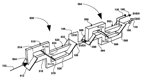
In FIG. 5A the first sub-stage includes filter 500 and the second sub-stage
includes filters 530 and 560. Filter 500 accepts an optical communication
signal 102 at
an interleave port 504 and provides optical outputs in the form of de-
interleaved odd
and even channel components of the signal at ports 106-108 respectively. The
second
sub-stage includes two filters 530,560. Each filter 530, 560 accepts a
corresponding
one of the de-interleaved odd and even components from the filter 500 of the
first sub-
stage at interleave ports 534, 564 respectively and performs further isolation
of the odd
and even channel components. Filter 530 outputs the odd channel components at
port
138 with the remaining port 136 serving as a dump port. Filter 560 outputs the
even
channel components at port 166 with the remaining port 168 serving as a dump
port.
The propagation direction of light determines whether the device performs as a
multiplexer or de-multiplexer.
Each filter in each sub-stage may include one or more filter cells. In the
embodiment shown the filter 500 of the first sub-stage includes two filter
cells,
510,520 serially coupled to one another between the interleave port 504 and de-
interleave ports 506-508 by couplers 512, 518, 522. Each filter cell includes
a pair of
delay paths. Within filter cell 510 delay paths 514, 516 are shown. One path
has a
shorter optical pathlength than the other and will be identified as the fast
path, with the
other identified as the slow path. Optical pathlength is a product of the
physical
distance "d" of an optical path and the index of refraction "n" along the
path. If path
514 and 516 are made from the same optical material then path 514 will have
the
longer optical pathlength and will thus be identified as the slow path. Path
516 would
in therefore be identified as the fast path. Light traversing the paths will
at any given
frequency experience a phase retardation proportionate to the differerice in
the
pathlengths between the slow and fast paths. The couplers 512, 518 define the
amount
of light which will be split/combined from/to each delay path within cell 510.
The
couplers 518,522 define the amount of light which will be split/combined
from/to each
delay path 524, 526 within cell 520.
The second sub-stage includes filters 530 and 560. Filter 530 includes two
filter cells, 540,550 serially coupled to one another between an interleave
port 534 and
CA 02438185 2003-08-11
WO 02/071103 PCT/US02/03717
de-interleave ports 136-138 by couplers 542, 548, 552. Each cell includes a
pair of
delay paths. The couplers 542, 548 define the amount of light which will be
split/combined from/to each delay path within cell 540. In an embodiment of
the
invention the coupling ratios are the same as the coupling ratios for the
filter 500 of the
5 first stage. The couplers 548,552 define the amount of light which will be
split/combined from/to each delay path within cell 550. Filter 560 includes
two filter
cells, 570,580 serially coupled to one another between an interleave port 564
and de-
interleave ports 166-168 by couplers 572, 578, 582. Each cell includes a pair
of delay
paths. The couplers 572, 578 define the amount of light which will be
split/combined
10 from/to each delay path within cell 570. The couplers 578, 582 define the
amount of
light which will be split/combined from/to each delay path within cell 580.
Delay paths may be defined by a range of optical elements including:
semiconductor waveguides and optical fibers for example. Delay paths may also
be
formed by discrete optical components such as those shown in the following
FIGS. 8-
15 10. The couplers may which split/combine light on the basis of intensity
may be
fabricated from transmissive/reflective dielectric coatings. Whether a sub-
stage
includes within a filter a single filter cell or multiple serially coupled
filter cells, at least
one of the cells, a.k.a. a fundamental cell, in each filter exhibits a free
spectral range
(FSR) which corresponds with the periodic frequency spacing between the odd or
even
channels, e.g. 100 GHz. In the embodiment shown in FIG. 5A cell 510 in the
first sub-
stage and cells 540, 570 in the second stage might for example serve as the
fundamental cells. The FSR of the second sub-stages fundamental cell(s) is
adjusted by
a fractional percent, or more particularly by an amount which results in the
optical
pathlength difference in the fundamental cell(s) of the second sub-stage which
diverges
from that of the fundamental cell of the first sub-stage by half the incident
wavelength.
This divergence results in the shift discussed above in connection with FIGS.
2-4,
which widens the stopbands of exhibited by the overall device.
FIG. 5B is an isometric view showing an alternate embodiment of the
mux/demux shown in FIG. 5A in which the second sub-stage comprises a single
filter
584 coupled to both the de-interleaved ports 106,108 of the first sub-stage
filter 500.
Filter 584 includes two interleaved input ports 586, 588 and four de-
interleaved output
ports 166, 138 and 136, 168. The latter two ports, 136,168 are dump ports. The
CA 02438185 2003-08-11
WO 02/071103 PCT/US02/03717
16
optical signals with both odd and even channel components are processed along
parallel optical paths within the ftlter 584. The $lter includes two filter
cells 590, 592.
Light is split/combined along the fast and slow path of the first filter cell
590 via
couplers 594, 596. Light is split/combined along the fast and slow paths of
the second
filter cell 592 by the couplers 596, 598.
In an embodiment of the invention suitable coupling percentages onto the fast
and slow paths are determined by the transmission/reflection ratios for each
of couplers
512, 518, 522 in the first filter. Symmetric coupling would for be satisfied
by couplers
with 50%/50% transmission/reflection. For asymmetrical coupling in accordance
with the current invention the following Table 1 sets forth two among many
acceptable
asymmetric coupling possibiIities for embodiments of the invention in which
each sub-
stage includes within a corresponding filter(s) two filter cells, interlaced
with three
couplers such as those shown in either FIGS. 5A-B.
Table 1
Input 15 Gpir 5low Ia 2" Cl2lr SIoW l0 3rd S1o+N %
intensity. % Tx Fast %; Tx Fast % % Tx Fast %
67% 28% 85%
Case 1 1 67% 33% 28% 72% 85% 15% ____.
. . . . . . .. .,,it~~t .. . .,ftYf . j(
. . . ' !~ . . .
. .. . . ~. . i : ..., ~ . . _ i 7 pl
59% 30% 91%
Case 2 1 59% 41% 30% 70% 91% 9%
FIG. 6 is an isometric view of an alternate embodiment of the invention in
which polarization couplers, ratlier than intensity couplers are used to
split/combine
optical signals within the mux/demux. The delay path pairs in this embodiment
may be
fabricated from optical fibers, semiconductor waveguides, or discrete micro-
optic
elements for example. Examples of the latter are described and discussed in
CA 02438185 2003-08-11
WO 02/071103 PCT/US02/03717
17
connection with the following FIGS. 8, 9. The polarization couplers may be
fabricated
from birefringent crystals or as dielectric coatings on optical elements for
example.
Examples of the latter are described and discussed in connection with the
following
FIGS. 8, 9.
In FIG. 6 the first sub-stage includes filter 600 and the second sub-stage
includes filters 630 and 660. Filter 600 accepts an optical communication in
the form
of a linearly polarized input signal 102 at an angle epl with respect to the
optical axis at
coupler 612. The optical axis may coincide with one or the other of the fast
and slow
axis. The filter 600 provides optical outputs in the form of de-interleaved
odd 106 and
even 108 channel components of the input signal. Each filter 630, 660 of the
second
sub-stage accepts a corresponding one of the de-interleaved odd and even
components
from the filter 600 of the first sub-stage at polarization couplers 642, 672
respectively
and performs further isolation of the odd and even channel components. The odd
and
even channel components are also communicated with the corresponding filter of
the
second stage in the form of linearly polarized light with input vectors of cp
and 0.5n +cp
with respect to the couplers 642, 672 respectively. Filter 630 outputs the odd
channel
components at port 138 with the remaining port 136 serving as a dump port.
Filter
660 outputs the even channel components at port 166 with the remaining port
168
serving as a dump port. The propagation direction of light determines whether
the
device performs as a multiplexer or demultiplexer.
Each filter in each sub-stage may include one or more filter cells. In the
embodiment shown the filter 600 of the first sub-stage includes two filter
cells, 610,
620 serially coupled to one another by couplers 612 and 618. Each filter cell
includes
a pair of delay paths. Within filter cell 610 delay paths 614, 616 are shown.
One path
has a shorter optical pathlength than the other and will be identified as the
fast path,
with the other identified as the slow path. Within cell 620 fast 624 and slow
626 delay
paths are also shown. Optical pathlength is a product of the physical distance
"d" of an
optical path and the index of refraction "n" along the path. If path 614 and
616 are
made from the same optical material, as in the case where a birefringent
crystal forms
the filter cell 610, thein whichever of the "e" or "o" ray experiences a
higher index of
refraction along the optical path will be characterized as the slow path.
Light
traversing the paths will at any given frequency experience a phase
retardation
CA 02438185 2003-08-11
WO 02/071103 PCT/US02/03717
18
proportionate to the difference in the pathlengths between the slow and fast
paths.
The amount of light coupled onto the slow and fast paths 614,616 in cell 610
is
determined by the angle cp of the input vector with respect to the optical
axis. Where
the cell is fabricated from a birefringent crystal the coupler, slow and fast
axis are
integral with the optical axis defined by the crystalline structure of the
birefringent
crystal. Where the cell if formed from a polarization coupler and fast and
slow paths
discrete from the polarization coupler then the optical axis is the optical
axis of the
coupler. In the embodiment shown light propagating in the forward direction
from
input 102 couples with the first cell at an angle cpl with respect to the
optical axis of
the coupler 612 and/or cell 610 and at an angle cp 2 with respect to the
optical axis of
the coupler 618 and/or cell 620.
The second sub-stage includes filters 630 and 660. Filter 630 includes two
filter cells, 640, 650 serially coupled to one another by couplers 642 and
648. Each
cell includes a pair of delay paths. Filter 660 also includes two filter cells
670, 680
serially coupled to one another by couplers 672 and 678. Each cell includes a
pair of
delay paths. The couplers of each filter in the second stage generally exhibit
the same
coupling ratios as the couplers in the filter of the first sub-stage. Delay
paths may be
defined by a range of optical elements including: birefringent crystals,
semiconductor
waveguides and optical fibers for example. Delay paths may also be formed by
discrete optical components such as those shown in the following FIGS. 8-9.
The
couplers may be fabricated from birefringent crystals, or polarization
sensitive
dielectric coatings, such as those discussed in connection with FIGS. 8-9.
Whether a sub-stage includes within a filter a single filter cell or multiple
serially coupled filter cells, at least one of the cells, a.k.a. a fundamental
cell, in each'
filter exhibits a free spectral range (FSR) which corresponds with the
periodic
frequency spacing between the odd or even channels, e.g. 100 GHz. The
fundamental
cell may in a multi-cell embodiment be placed in any sequence with respect to
the other
cells of the filter. In the embodiment shown in FIG. 6, cell 610 in the first
sub-stage
and cells 640, 670 in the second stage might for example serve as the
fundamental
cells. The FSR of the second sub-stages fundamental cell(s) is adjusted by a
fractional
percent, or more particularly by an amount which results in an optical
pathlength
difference in the fundamental cell(s) of the second sub-stage which diverges
from that
of the fundamental cell of the first sub-stage by half the incident
wavelength. This
CA 02438185 2003-08-11
WO 02/071103 PCT/US02/03717
19
divergence results in the shift discussed above in connection with FIGS. 2-4,
which
widens the stopbands of exhibited by the overall device.
The odd and even channel sets within an optical signal experience the
filtering
of the fundamental cell 610 of the first sub-stage differently. The
fundamental cell of
the first sub-stage operates as a full waveplate to a selected one of an odd
channel set
and an even channel set and as a half-waveplate to a remaining one of the odd
set and
the even set. Within the fundamental cell(s) 640, 670 of the second sub-stage
the
opposite filtration effect is experienced by the odd and even channel sets.
The
fundamental cell(s) of the second sub-stage operate as a half-waveplate to the
selected
one of the odd set and the even set and as a full waveplate to the remaining
one of the
odd set and the even set. Where a selected channel set odd/even experiences
the
fundamental cell as a half waveplate linearly polarized light with frequency
components
associated with the selected channel set which enters the cell with one
polarization
vector, emerges from the cell with a relative phase shift of 1/~ ar and a
rotation in the
associated polarization vector in the direction of the optical axis of the
coupler in an
amount 2cp where cp is the angle between the input polarization vector and the
optic
axis of the cell. Where a selected channel set odd/even experiences the
fundamental
cell as a full waveplate linearly polarized light with frequency components
associated
with the selected channel set which enters the cell with one polarization
vector,
emerges from the cell with the same polarization vector.
In the embodiments of the invention shown in FIG. 6 as well as in FIGS. 7A-D
suitable coupling percentages onto the fast and slow paths are determined by
the angle
cp between the input polarization vector and the optic axis of the
ce11/coupler. The
following Table 2 shows suitable angles for both symmetric (Case 1) and
asymmetric
coupling (Cases 2-3) for embodiments of the invention in which each sub-stage
includes within a corresponding filter(s) two filter cells and corresponding
couplers as
shown in FIG. 6.
CA 02438185 2003-08-11
WO 02/071103 PCT/US02/03717
Table 2
lnpuf 15Gplr Stavit 2 Cplr Slciw % 3' ~plr Sbw0o
int~nsity ~~ q> Fast %' sp ~ Past lo -~. Fast = ~o 50% 25% 93%
Case 1 1 45 50% -15 75% 0 7 fo
Symmetric
r,njm ; } .,
. . . . .._4r. . . . .
. : {, . . . .i -.. . ~i .: il ..._ ...,.._ . . . . .: . r~.n .,~IN ...:-.
rri'} ... .-.. .
-.. -. ._. __.. _.. -.._ _ - _ - .j.-._. .__
59% 30% 91%
Case 2 1 40 41% -17 70% 0 9%
Asymmetric
67% 29% 85%
Case 3 1 35 33% -2,2.5 71% 0 15%
As mmetric
FIG. 7A is an isometric view showing an alternate embodiment of the
mux/demux shown in FIG. 6. FIGS. 7B-C are top/plan and side/elevation views of
the
5 mux/demux. FIG. 7D shows polarization diagrams 776-798 for light propagating
through the mux/demux. In this embodiment of the invention the second sub-
stage
comprises a single filter 730 optically coupled with the polarized outputs of
the first
sub-stage filter 700.
On the forward/demux path an optical signal 102 may be introduced via an
10 optical fiber into lens 702. Lens 702 may include a Graded Index of
Refraction
(GRIN) or other lens system. The lens collimates/focuses light depending on
the
propagation direction from/to the beam splitter 704. The beam splitter may be
fabricated from a birefringent crystal with an optic axis oriented to effect a
walk-off of
the forward beam onto waveplates 706-708. The waveplates are broadband and
have
15 optical axis oriented to effect a linearization of the polarization vectors
of the two rays
formed by the beam splitter. The linearly polarized rays are then introduced
into the
filter 730 of the first sub-stage 700 and specifically into cell 710 thereof.
Cell 710 is, in
this embodiment of the invention, fabricated from dielectric polarization
dependent
couplers on opposite ends of a pair of fast and slow delay paths. The general
cell
20 structure for this and subsequent filter cells, 720, 740, 750 is set forth
in detail in the
CA 02438185 2003-08-11
WO 02/071103 PCT/US02/03717
21
following FIGS. 8-9. Light is coupled between filter cell 710 and filter cell
720. The
rotation angle cp of the filter cells 710, 720 with respect to the input
polarization vector
of each of the two rays into which the optical signal has been split
determines the
coupling of light onto the fast and slow paths of each cell. Odd and even
signal
components are output by filter cell 720. The passbands for the odd and even
channel
components at this point correspond with the passbands discussed above in
connection
with FIGS. 2A, 4A and 4E.
Between the first sub-stage and the second sub-stage a beam splitter 722 and
waveplates 724-726 are positioned. The beam splitter splits the odd and even
signal
1o outputs from the first sub-stage into component vectors which are then
linearized by
waveplates 724-726. The component vectors for the odd and even channels are
then
introduced into the second sub-stage 730 where they will be further isolated.
The
second sub-stage includes two .filter cells 740, 750 serially coupled with one
another
One of these cells a.k.a. the fundamental cell, as also one of the cells of
the first stage,
exhibits a free spectral range corresponding with the channel spacing between
adjacent
odd or even channels. The fundamental cell of the first sub-stage and the
second sub-
stage diverge from one another in optical pathlength difference by the above
discussed
amount of 1/~ the incident wavelength. This produces the shift which results
in
dispersion reduction/compensation. Light propagating from the filter cell 750
of the
second sub-stage propagates through an optical beam bender 762 formed from an
inclined surface. This has the effect of linearizing the rays as they are
presented to the
combined waveplates 764 and splitter/combiner 766. The waveplates
orthogonalize
the odd and even channel components and pass them to the splitter/combiner. On
the
forward /demux path this results in two arbitrarily polarized beams
corresponding with
the de-interleaved odd and even channel signal components. These are focused
via
lens 768 oiito optical fiber or other suitable connectors which accept the odd
and even
channel components 138, 166 respectively.
In the embodiment of the invention shown in FIG. 7A-D the odd and even
channel sets experience the first sub-stage and second sub-stage differently.
The
fundamental cell , e.g. cell 720, of the first sub-stage 700 operates as a
full waveplate
to a selected one of an odd channel set and an even channel set and as a half-
waveplate to a remaining one of the odd set and the even set. Within the
fundamental
cell, e.g. cell 750 of the second sub-stage 730 the opposite filtration effect
is
CA 02438185 2003-08-11
WO 02/071103 PCT/US02/03717
22
experienced by the odd and even channel sets. The fundamental cell of the
second sub-
stage operates as a half-waveplate to the selected one of the odd set and the
even set
and as a full waveplate to the remaining one of the odd set and the even set.
FIG. 8A is an isometric view of an optical filter cell 1100 with couplers
employing polarization dependent beam splitting linked by a pair of delay
paths 1150
and 1146,1148,1152. Each coupler transmits and reflects light depending on the
input
properties of the light. In the embodiment of the invention shown in FIG. 8A,
each
coupler is polarization sensitive and includes "P" and "S" polarization axis
orthogonal
to one another. A first coupler is positioned in the propagation path of
incoming
polarized light and transmits and reflects components of inconiing polarized
light
aligned with the "P" and "S" polarization axis of the coupler respectively.
Light
transmitted and reflected by the coupler follows two distinct delay paths, one
for
transmitted light and the other for reflected light. Where incoming light is
orthogonally
polarized, the first coupler provides configurable amounts of coupling and
cross-
coupling of each of the orthogonal polarization vectors of the incoming light
with
either of the pair of delay paths. A second coupler positioned at a location
where the
two distinct delay paths intersect reverses the process and re-aligns light
with
orthogonal polarization vectors onto a common propagation axis.
The cell is shown within an "x,y,z" Cartesian coordinate system. The cell
includes opposing optical glass blocks 1110, 1130 displaced from one another
along
the z axis with the optical elements 1120A-B covering the span between the
blocks.
Optical glass block 1110 is shown with a reflector 1112 and a polarization
dependent
beam splitter 1114 displaced from each other in a direction defined by the y
axis.
Optical glass block 1130 is shown with a reflector 1132 and a polarization
dependent
beam splitter 1134 displaced from each other in a direction defined by the y
axis. The
polarization dependent beam splitters have "S" polarization axes 1116 and 1136
respectively which are aligned with one another and in the orientation of the
cell that is
shown, also aligned with the x axis. The "P" polarization axis of each
polarization
dependent beam splitter are orthogonal to the "S" axis. Polarized light input
at the
first port 1102 will couple with both the P and S axis of the first coupler
1114, a
polarization beam splitter in amounts which corresponded with the relative
angular
rotation between the polarization vector(s) of the polarized input and the
orthogonal P
CA 02438185 2003-08-11
WO 02/071103 PCT/US02/03717
23
and S polarization axis of the beam splitter. The component of a polarized
input which
projects onto the S polarization axis of the beam splitter will be reflected
by the beam
splitter. The component of a polarized input which projects onto the P
polarization
axis of the beam splitter will be transmitted by the beam splitter. Between
the couplers
an optical element 1120 is shown.
Each optical glass block 1110,1130 may in fact be fabricated from two pairs of
prisms. In the case of block 1110 the polarization dependent beam splitter
1114 may
be formed from a first pair of prisms at right or other complementary angles
to one
another. These may be affixed to one another, e.g. cemented, to minimize wave
front
distortion. The hypotenuse of one of the prisms is coated with a multi layer
dielectric
polarizing beam splitter coating. The prisms are then affixed to one another,
to form a
first rectangle, the exterior surfaces of which may be antireflection coated
(AR) to
minimize surface reflection losses. A second pair of prisms may be used to
form the
reflector 1112. The hypotenuse of one of this second pair of prisms is coated
with a
reflective dielectric coating, and cemented to the hypotenuse of the other of
the second
pair of prisms. The hypotenuses of this second pair of prisms are then affixed
to one
another as well to form a second rectangle, the exterior surfaces of which may
also be
AR coated. The two rectangles formed by the two pairs of prisms may then be
affixed
to one another to form the glass block 1110. A similar technique may be used
to
fabricate the second block 130.
The cell couples light bi-directionally between a first port 1102 and a second
port 1104 displaced from one another in a direction defined by the z axis. For
purposes of illustration, polarized light 1140 is shown entering the cell at
the first port
and exiting as a polarized output beam 1154 at the second port though the
propagation
in the opposite direction is also supported. The cell is also highly
directional so that
light propagating in one direction is independent of the light propagating in
the reverse
direction. The polarized light beam 1140 may be arbitrarily, circularly or
linearly
polarized. In the example shown, beam 1140 is linearly polarized with a
polarization
vector 1144 at an angle cpi with respect to the "S"polarization axis 1116 of
the cell. As
the beam 1140 enters the cell it is accepted onto either of two distinct P and
S delay
paths 1150 and 1146, 1148, 1152 respectively. These delay paths link the
polarization
dependent beam splitters 1114, 1134. The amount of light that is coupled onto
either
CA 02438185 2003-08-11
WO 02/071103 PCT/US02/03717
24
delay path is determined by the angle (pl of the incoming beam vector with
respect to
the S polarization axis of the cell. In the example shown, light from
polarization vector
1144 in amounts proportionate to sin(q)i ) and cos(cpi ) will couple to the P
and S delay
paths respectively. Rotation of the cell about the propagation path, e.g. the
z axis, of
the beam 1140 can be used to vary the coupling percentages or ratios between
the
incoming light and the P and S delay paths. Where incoming light includes
orthogonal
polarization vectors the coupling of either vector will be determined by
projecting that
vector onto the P and S polarization axis of the polarization beam splitter as
well. The
polarization beam splitters 1114,1134 thus serve as couplers which provide
configurable amounts of coupling and cross-coupling of incoming beams with
either of
the pair of delay paths.
The amount of delay on the P and S delay paths are p, and 8s, respectively.
The delay of each path is determined by its corresponding optical path length.
The
optical path length of each path is the sum of the product of physical
dimension and the
index of refraction of all the optical elements on each of the two distinct P
and S delay
paths 1150 and 1146,1148,1152 respectively. The delay difference for the cell
is
proportional to the difference in the optical path lengths between the P and S
delay
paths. The delay difference exhibits itself in the optical properties of the
output beam
1154. That output beam exhibits the interference pattern produced by the re-
coupling
of the P and S delay paths by the second of the polarization beam splitters
1134 into a
single output beam. The output beam includes orthogonal polarization vectors
1156-
1158. Each contains complementary periodic stop bands and pass bands of the
other
with center wavelengths the spacing between which is inversely related to the
delay
difference between the P and S delay paths. In other words the larger the
delay
diiference the smaller the wavelength spacing which the optical filter cell
can resolve.
The first vector 1156 contains pass bands with center wavelengths at even
integer
multiples of the periodic interval established by the delay difference. The
second
vector 1158 contains pass bands with center wavelengths at odd integer
multiples of
the periodic interval established by the delay difference.
The cell may be provided with an appropriate lens, e.g. a GRIN lens or other
suitable lens, and a linear polarizer coupled to the first port to linearly
polarize
arbitrarily polarized incoming light and to direct it to the first port. At
the opposite
CA 02438185 2003-08-11
WO 02/071103 PCT/US02/03717
end, a beam displacer/combiner may be coupled with the second port to displace
and
combine orthogonally polarized odd and even channel components 1156-1158 of an
optical beam depending on the propagation direction of the light beam. An
appropriate lens(es), e.g. GRIN, may also be added at this end to focus and
collimate
5 the light from the beam displacer/combiner depending on the propagation
direction.
The resultant system may serve as either or both a multiplexer or a
demultiplexer
depending on a propagation direction of the light.
In an alternate embodiment of the invention there may be a single reflector
replacing reflectors 1112 and 1130 to bend the S delay path between the two
10 polarization beam splitters 1114 and 1134. In still another embodiment
additional
reflectors may be added.
In an alternate embodiment of the invention an opposing pair of back-to-back
birefringent crystals may be used instead of the polarization beam splitters
to split
incoming light into an "e" and an "o" ray delay path corresponding with "S"
and "P"
15 delay paths respectively. The principal planes of the pair of crystals
would be aligned
in a common plane witli the optical axis of each birefringent crystal at
substantially
complementary angles to one another so as to cause a splitting and recombining
of the
e and o ray delay paths.
FIG. 8B is an isometric view of an optical filter cell 1106 with couplers
20 employing intensity dependent beam splitting linked by a pair of delay
paths 1170 and
1166,1168,1172. This cell is also shown within an "x,y,z" Cartesian coordinate
system. The cell includes many of the features of the cell shown in FIG. 8A
with the
exception that the coupling function is here performed by partial reflectors
1164,1174
which form intensity beam splitters. The cell includes opposing optical glass
blocks
25 1110, 1130 displaced from one another along the z axis with the optical
element 1120
covering the span between the blocks. Optical glass block 1110 is shown with a
reflector 1112 and the intensity beam splitter 1164 displaced from each other
in a
direction defined by the y axis. Optical glass block 1130 is shown with a
reflector
1132 and an intensity beam splitter 1174 displaced from each other in a
direction
3o defined by the y axis. Between the couplers an optical element 1120 is
shown.
CA 02438185 2003-08-11
WO 02/071103 PCT/US02/03717
26
Each optical glass block may in fact be fabricated from two pairs of prisms.
In
the case of block 1110 the intensity beam splitter 1164 may be formed from a
first pair
of prisms at right or other complementary angles to one another, which are
cemented
together to minimize wave front distortion. The hypotenuse of one of the
prisms is
coated with a multi layer dielectric beam splitter coating which exhibits
configurable
amounts of transmission and reflection of an incident beam. The prisms are
then affixed
to one another, e.g. cemented together, to form a first rectangle, the
exterior surfaces
of which may be antireflection coated (AR) to minimize surface reflection
losses. A
second pair of prisms may be used to form the reflector 1112. The hypotenuse
of one
of this second pair of prisms is coated with a reflective dielectric coating,
and affixed
to the hypotenuse of the other of the second pair of prisms. The hypotenuses
of this
second pair of prisms are then affixed to one another as well to form a second
rectangle, the exterior surfaces of which may also be AR coated. The two
rectangles
formed by the two pairs of prisms may then be affixed to one another to form
the glass
block 1110. A similar technique may be used to fabricate the second block
1130.
The cell 1102 couples light bi-directionally between first/second ports 1180-
1182 and the third/fourth ports 1184-1186. For purposes of illustration
optical beams
1160-1162 are shown entering the cell at the first and second ports 1180-1182
respectively and exiting the cell as beams 1178-1176 at the third and fourth
ports
1184-1186 respectively. Propagation in tlie opposite direction is also
supported. The
cell is also highly directional so that light propagating in one direction is
independent of
the light propagating in the reverse direction. In the example shown, beam
1160 enters
the cell at port 1180 and beam 1162 enters the cell at port 1182. Each beam is
accepted onto either of two distinct transmission (Ti) and reflection (Ri)
delay paths
1170 and 1166, 1168, 1172 respectively. These delay paths link the intensity
beam
splitters 1164, 1174. The amount of light that is coupled from the inputs at
ports 1180
and 1182 onto either delay path by each beam is determined by the beam path
and the
ratio or percentage of transmission and reflection of the beam splitter 1164.
The
amount of light that is coupled from the either delay path to the output at
ports 1184
and 1186 is determined by the beam path and the ratio or percentage of
transmission
and reflection of the beam splitter 1174. The percentage of transmission and
reflection
is an optical property that can be precisely specified. The intensity beam
splitters
CA 02438185 2003-08-11
WO 02/071103 PCT/US02/03717
27
1164,1174 thus serve as couplers which provide configurable amounts of
coupling and
cross-coupling of incoming beams with either of the pair of delay paths.
The amount of delay on the Tl and Rl delay paths 1170 and 1166, 1168, 1172
are 8Ti and ORi respectively. The delay of each path is determined by its
corresponding
optical path length. The optical path length of each path is the sum of
product of the
physical dimension and the index of refraction of all the optical elements on
each of the
two distinct delay paths. The delay difference for the cell is proportional to
the
difference in the optical path lengths between the R, and Ti delay paths. The
delay
difference exhibits itself in the optical properties of the output beams 1176-
1178. The
output beams exhibit an interference pattern produced by the re-coupling of
the Rl and
Tl delay paths by the second of the beam splitters 1174. Each output beam
contains
complementary periodic stop bands and pass bands of the other with center
wavelengths the spacing between which is inversely related to the delay
difference
between the Rl and T1 delay paths. In other words the larger the delay
difference the
smaller the wavelength spacing which the optical filter cell can resolve.
Output beam
1176 contains pass bands with center wavelengths at even integer multiples of
the
periodic interval established by the delay difference. Output beam 1178
contains pass
bands with center wavelengths at odd integer multiples of the periodic
interval
established by the delay difference.
The single cell 1102 may serve as either or both a multiplexer or a
demultiplexer depending on a propagation direction of the light.
For each of the optical filters discussed above it may be necessary to adjust
the
center wavelength and free spectral range of any given cell or set of delay
paths. This
can be accomplished by tilting of the cell about the x axis normal to the
propagation
path, or by tilting each of the component within the cell resulting a net
change of
effective optical path length difference. This will allow a coarse tuning to
the
appropriate free spectral range followed by a shifting, i.e. a fine tuning, of
the center
wavelength of all the pass bands generated by each cell or delay path.
FIG. 8C is an isometric view of an optical filter cell shown in FIG. 8A with
one
of the optical elements, i.e. element 1120AB, configured for adjustment of the
center
wavelength and free spectral range of the filter. Optical element 1120AB is
shown
cleaved into a pair of complementary wedges 1120A and 1120B. As each wedge is
CA 02438185 2003-08-11
WO 02/071103 PCT/US02/03717
28
moved in opposing directions along the x axis the optical path length of delay
path
1150 is altered. This results in a shift in the center wavelength and a change
in the free
spectral range of the cell. Once the cell exhibits the desired center
wavelength the
wedges 1120A, 1120B are fixed relative to the blocks 1120 and 1130.
FIG. 8D is an isometric view of an optical filter cell shown in FIG. 8B with
one of the optical elements configured for adjustment of the center wavelength
and
free spectral range of the filter and with an alternate coupler configuration.
As
discussed above in connection with FIG. 8C the cleaving of element 1120 into
wedges
1 120A and 1120B provides a means for shifting the center wavelength and
adjusting
the free spectral range of the cell.
. FIG. 8D also introduces an alternate configuration for the blocks 1110 and
1130 shown in FIGS. 8A-B. This alternate block configuration is shown in the
context
of intensity dependent beam splitting as introduced in FIG. 8B, and may be
applied
with equal advantage to the polarization dependent beam splitting shown in
FIG. 8A.
The couplers 1164,1174 are defined on the corresponding external base faces of
a pair
of opposing blocks 1188 and 1190. Each block 1188,1190 is configured with an
upper
angular portion on the corresponding external surfaces of which the reflectors
1112,1132 respectively are defined.
FIG. 8E is an isometric view of an optical filter cell shown in FIG. 8B with
one
of the optical elements configured for adjustment of the center wavelength and
free
spectral range of the filter and with an alternate coupler configuration. As
discussed
above in connection with FIG. 8C the cleaving of element 1120 into wedges
1120A
and 1120B provides a means for shiffing the center wavelength and adjusting
the free
spectral range of the cell.
FIG. 8E also introduces still another configuration for the blocks 1110 and
1130 shown in FIGS. 8A-B. This alternate block configuration is also shown in
the
context of intensity dependent beam splitting as introduced in FIG. 8B, and
may be
applied with equal advantage to the polarization dependent beam splitting
shown in
FIG. 8A. In this embodiment of the invention the block structure is dispensed
with and
each coupler 1164,1174 is defined on its own discrete substrate. Suitable
substrates
include any suitable transparent medium, e.g. optical glass or a semi-
conductor.
CA 02438185 2003-08-11
WO 02/071103 PCT/US02/03717
29
Similarly, reflectors 1112 and 1132 are realized on their own discrete
substrate, which
in this case does not need to be transparent. Each coupler and reflector is
positioned
with respect to one another by a suitably stable frame, not shown.
FIG. 9A-B are isometric and end views respectively of a multi-cell
implementation of the optical filter cell shown in FIG. 8A. Two cells 1100 and
1200
are shown coupled serially to one another in sequence. This concept of
serially
coupling cells allows an optical filter to exhibit a more complex transfer
function than
the simple sinusoidal output provided by the single cell shown in FIG. 8A. In
this
example the delay paths provided by cell 1200 and their delay difference are
larger than
the delay paths and delay difference provided by the cell 1100. This result
can be
achieved either by fabricating cell 1200 from the same optical elements as
cell 1100
with an increase in the physical length of the elements or by fabricating cell
1200 from
optical elements with higher indices of refraction than those of cell 1100
thus
maintaining the same form factor for both cells.
The combination of first cell and subsequent cells can be looked at as
establishing by the difference between their delay paths the fundamental
sinusoidal
harmonic for the sequence and higher order harmonics. In an embodiment of the
invention this objective is achieved by designing one of the cells in the
sequence with a
FSR corresponding with the desired fundamental harmonic and with others of the
cells
designed with FSRs which are integer fractions of the base FSR. The
coefficients or
amplitude of each harmonic are provided by varying the coupling
ratio/percentage/coefficients between a polarized input to a cell and the P
and S
polarization axes of the cell as provided by the corresponding polarization
beam
splitter. The coupling coefficients are varied by tilting of a cell about the
propagation
path of a polarized input to each cell.
Cell 1100 includes the components described above in connection with FIG.
8A. Cell 1200 includes couplers 1214,1234 employing polarization dependent
beam
splitting linked by a pair of delay paths 1250 and 1246, 1248, 1252. The cell
1200
includes opposing optical glass blocks 1210, 1230 displaced from one another
along
the z axis with the optical element 1220 covering the span between the blocks.
Optical
glass block 1210 is shown with a reflector 1212 and a polarization dependent
beam
splitter 1214 displaced from each other in a direction defined by the y axis.
Optical
CA 02438185 2003-08-11
WO 02/071103 PCT/US02/03717
glass block 1230 is shown with a reflector 1232 and a polarization dependent
beam
splitter 1234 displaced from each other in a direction defined by the y axis.
The
polarization dependent beam splitters have "S" polarization axis which are
aligned with
one another. Between the couplers an optical element 1220 is shown. The
various
5 components are shown on top of base 1206.
Polarized beam 1140 has, in the example shown, a linearly polarized input with
a vector 1144. This beam enters the cell 1100 at the first port 1102, is
reflected and
transmitted by polarization beam splitter 1114 onto one end of the pair of
delay paths
8s, and Opi. At the opposite end of the delay paths reflection and
transniission by the
10 polarization beam splitter 1134 produces a common output beam 1154 which
exits the
cell 1100 at port 1104. Port 1104 of the first cell couples with port 1202 of
the next
cell 1200 in the sequence. Thus, the beam 1154 output from the first cell
enters the
second cell 1200 where it is reflected and transmitted by polarization beam
splitter
1214 onto one end of the pair of delay paths 6s2 and r2. At the opposite end
of the
15 delay paths reflection and transmission by the polarization beam splitter
1234 produces
a common output beam 1254 whicli exits the cell 1200 at port 1204, with
orthogonal
polarization vectors 1256-1258 with odd and even components, respectively. The
process can be repeated to form a longer sequence of cells and a more complex
optical
filter transfer function.
20 FIG. 9C is a side elevation view of the delay paths of the multi-cell
implementation shown in FIGS. 9A-B. The delay introduced into light passing
along
any delay path is a function of the optical path length of the optical
elements which
comprise the delay path. Optical path length "L" of an optical element is
expressed as
the product of the physical distance "d" traversed by a beam propagating
through the
25 element multiplied by the index of refraction "n" of the element. Where
multiple
optical elements are involved the individual contributions to the optical path
length
from the individual elements are summed. For purposes of the current invention
optical elements include: a vacuum, a gas, a liquid, a solid or a plasma along
the
propagation path. The index of refraction of a medium identifies the ratio of
the speed
30 of light in a vacuum to that of light in the medium. Where the optical path
length
varies as here between two delay paths one path is said to be faster/slower
than the
other and there is said to be a delay difference between the two.
CA 02438185 2003-08-11
WO 02/071103 PCT/US02/03717
31
Beam 1140 propagates through the first cell 1100 across delay paths Opi and
8s, and through the second cell 1250 across delay paths OP2 and Os2. Delay
path 8P,
comprises optical elements defined by optical path length L15-L17. Delay path
Osi
comprises optical elements defined by optical path lengths Llo-L14. Delay path
6P2
comprises optical elements defined by optical path length L25-L27. Delay path
Os2
comprises optical elements defined by optical path lengths L20-L24: In the
embodiment
shown the optical elements defined by optical path lengths L12 and L22 include
air/gas/vacuum. The remaining optical elements may be fabricated from various
types
of optical glass including: BKx, fused silica, SFx. By proper design of delay
paths the
fundamental and higher order harmonics for the optical filter may be
established.
The delay for the delay paths 8P1 and 8s1 in the first filter 1100 are
expressed as
a function of the optical path lengths of each path in the following Equations
4-5
respectively.
V t=j
Equation 4: BS1 = 2z -~, din1
c ~=1
~djnj)
Equation 5: 8P1 = 29Z v C j=1
where c and v are the frequency and velocity of light in free space and where
I and J
2o are the number of optical elements which make up the delay paths with
delays OS, and
0p1 respectively. For each of the I optical elements: vacuum, gas, plasma,
liquid or
solid which make up the delay path 85, the i~' element has a physical length
di and an
index of refraction n;. For each of the J optical elements: vacuum, gas,
plasma, liquid
or solid which make up the delay path 8P1 the j"' element has a physical
length dj and an
index of refraction nj. Optical elements include the optical coatings
associated with
polarization or intensity dependent beam splitters, which also contribute to
optical
pathlength and phase accumulations.
The delay difference between the two paths is expressed in Equation 6.
CA 02438185 2003-08-11
WO 02/071103 PCT/US02/03717
32
I_I ~~
Equation 6: 8s1 - ePl = 2)r ~Idnl -Edjn j
i=1 j=1
The delay difference for the cell is proportional to the difference in the
optical
path lengths between the S and P delay paths. Similar considerations apply in
determining the delays and delay differences for the pair of delay paths in
the second
cell 1200.
The optical path length difference between the two delay paths in a cell,
corresponds inversely with the free spectral range (FSR) generated by the cell
as
evidenced in the orthogonal vector components of the output beam from the
cell. This
relationship is set forth in the following Equation 7.
Equation 7: FSR = L J cj_' 2~ v
(FL;-~C~ I 1=I 8 -8
s p
dn= - E d.in.i
i=1 j=1
where LI and Lj are the total optical path length of the I and J elements
which make up
the corresponding delay paths 8si and Opi.
For an optical mux/demux the FSR should be a constant perhaps equal to the
channel spacing, e.g., 100 GHz. Using Equation 7 the delay difference required
to
generate this result can be determined, and from it a solution to the optical
path lengths
for each of the delay paths.
FIG. 9D is a side elevation view of the variable coupling between cells of the
multi-cell implementation shown in FIGS. 9A-B. Coupling is used to control the
amount an input of polarized light that will be projected onto the S and P
delay paths
of a corresponding cell. Three coupling views 1260, 1262 and 1264 are shown at
appropriate locations at the input to cell 1100, the interface between cells I
100 and
1200 and at the output of cell 1200 respectively. The three views 1260-1264
are from
the output port 1204 looking back along the propagation path of the input beam
1140.
In the first of the coupling views 1260, the polarized input is shown with a
single input
vector 'P' and the orthogonal polarization axis P 1 and S 1 of the first cell
1100 are
shown. The input I may include orthogonal input vectors. The amount of light
that is
CA 02438185 2003-08-11
WO 02/071103 PCT/US02/03717
33
coupled onto either delay path in the first cell is determined by the angle
cpi of the
incoming beam vector with the S polarization axis of the cell. In the example
shown
light from polarization vector 1144 in amounts proportionate to sin ((pi) and
cos(cpi )
will couple to the P and S delay paths respectively. Rotation of the cell
about the
propagation path of the beam 1140 can be used to vary the coupling percentages
or
ratios between the incoming light and the P and S delay paths. In the next
coupling
view 1262, light from the output port of cell 1100 is coupled with the input
port of cell
1200. The orthogonal polarization vectors P1,S1 present in the output of the
first cell
are shown along with the orthogonal polarization vectors P2,S2 which are
defined by
the coupler of the next cell in the sequence, i.e. cell 1200. The amount of
light that is
coupled onto either delay path in the second cell is determined by the angle
e02 between
the two sets of orthogonal vectors for the input and the cell 1200. The last
coupling
view 1264, shows both the orthogonal polarization vectors P2, S2 present in
the output
of the second cell along with a second set of orthogonal polarization vectors
Po,So .
This last orthogonal vector set is used to represent output optics used to
separate the
orthogonal vectors within the single output beam into two discrete beams (not
shown).
The amount of light coupled onto the output beams is defined by the angle cQ3
between
the two sets of orthogonal vectors.
FIG. 9E shows the individual transforms 1288 associated with each of the four
2o distinct delay paths from the input port 1102 to the output port 1204. The
number of
discrete paths in a multi-cell sequence of N cells with two delay paths
between each
equals 2N. For two cells there are 22 or 4 discrete paths between an input and
an
output. The first of these paths is along delay paths 8si and 6s2 in the first
cell 1100
and the second cell 1200 respectively. The second of these paths is along
delay paths
8s, and 6P2. The tliird of these paths is along delay paths 8P, and 6s2. The
fourth of
these paths is along delay paths 8P, and 8P2. The transfer function for the
optical filter
in single or sequential cell embodiments is the sum of the individual transfer
functions
associated with each discrete path from input to output. Transfer functions:
1288,
1290, 1292, 1294 are shown for the lt to 4th paths discussed above. Each
transfer
function includes two terms 1296-1298. The first term 1296 corresponds to a
coefficient in a Fourier series with the coefficient magnitude proportional to
the
product of the coupling or cross coupling coefficients along the particular
path. The
CA 02438185 2007-07-23
WO 02/071103 1'CT/C!'S02/03717
34
second te.nn 1298 corresponds to the firequency coinponent associated vvith
that
coefficient. The frequency component corresponds with the sum of the delays
along a
corresponding path. This in turn corresponds with the optical path lengths
along each
path. The sum of all the transfer functions forms a truncated Fourier series
which fully ~
S defiuces the optioa{ filter.
Li axt embodiment of the invention a tnuh.i-cell design itacludes: a first
cell of
100 GHz FSR and a 2pd cellof 50 GHz FSit can be used to form a polarization
type
square top conib filters. This fx,lter can split tui optical stream ivith 50
GHz chaenel
spacing into two separate oplical streams with odd and even 100 GHz channel
spaciixg
respectively or combining two optical stream witli 100 GI4z odd and even
channel
spacing respectively iulto zui optical stream with 50 GrYdT chanatel spacing.
The I' angle
q>1 can substantially equal to 45 degree and 2aid angle 02 ean substa13tially
equal to (45
+ 22.5) degree. Sitalarly, a first cell of 100 GT-lz FSR and a 2"d ceIl of 50
CxIizk'SR
can be used to forim a intensity type of'square top comb filters. '1'}te 1"
splitting ratio
iS equals substantially to 50/50% aatd the 2d splitting ratio equals
Coe(45+22_5)/
Sina(45+22.5=). fn still another embodiment of the invention a first stage
with a
plurality of cells and a second stage with a plurality of cells can be coupled
together to
fintber clean up the signal_ Yn a multi-cell elnbodumertt a scluare top filter
funetion may
be achieved by choosing one cell with the base F5R and with the FSRs of the
2o remainirr,g cells standing in relation to the FSR of'the base c:ell as
integer fractional
tnultiples thereof.
Further teachings on secluontially coupled optical filter cells znay be found
in
either of the two following references. See S.E. Harris et al., Qnt cal
Network Svnt]kesis
Using,VlrefrinAent Crys=tals, JOURNAL OP T1-lE OPTICAL SOCIETY OF AMP',RICA,
25 VOLUNIE 54, Number 10, October 1964 for a general discussion of transfer
functions
i-elated to birefrxngent crystals. See C.H. Henry et aJ. U.S. Patent No.
5,596,661 entitled
"Monolttlaic Optical Waveguide Filters based on FourierEzpansioiz" issued on
Jan. 21,
1997 for a general discussion of transfer functions related to waveguides.
CA 02438185 2003-08-11
WO 02/071103 PCT/US02/03717
Passive Thermal Stabilization
The typical application of optical filters constructed using the above
techniques
is an optical mux/demux. In order for that device to function properly it must
create
the desired stop bands and pass bands for the odd and even channels which it
5 separates. For current telecommunication applications the filter would be
designed
with a constant FSR perhaps equal to the channel spacing, e.g., 100 GHz. An
optical
filter with this FSR would generate the required stop bands and pass bands in
each of
the orthogonal polarization vectors present on the output. One of the
orthogonal
output vectors would contain the pass bands associated with the center
wavelengths of
10 the odd channels. The other of the orthogonal output vectors would contain
the pass
bands associated with the center wavelengths of the even channels.
Temperature variations in a mux/demux that may effect the performance may
result from the environment or from the power transmitted through the device.
Tlus
can result in the periodic odd and even pass bands generated by the optical
filter
15 moving out of alignment with the selected grid, e.g., the ITU grid. This is
primarily
because the center wavelength of a pass band slips with temperature. This
misalignment results in attenuation of signal strength, cross talk and
ultimately loss of
transmission/reception capability until the optical filter returns to its
original
temperature. In practice therefore, the optical filters and devices fabricated
therefrom
20 must be thermally stable across a range of temperatures.
One solution is to flatten the pass bands of the filter. Multi cell filter
designs
such as those discussed above allow the pass bands to exhibit higher order
harmonics
in the form of non-sinusoidal pass band profiles, a.k.a. "flat tops" (See FIG.
11). The
close spacing between the channels in a WDM, makes it desirable to design a
WDM
25 with flat pass bands in order to increase the error tolerance to
temperature induced
shifts in the pass bands. Even with flat top filter profiles temperature
stabilization is
still required due to the precise telecommunication chazuiel spacing.
One solution is to actively stabilize the temperature of the multiplexer/de-
multiplexer using a heater or cooler and a closed loop feedback of temperature
or
30 wavelength. This solution can be expensive and may increase the form factor
of the
mux/demux. Nevertheless, the current invention may be practiced with active
temperature stabilization. A possible benefit to active temperature
stabilization is that
CA 02438185 2003-08-11
WO 02/071103 PCT/US02/03717
36
the optical elements which make up each pair of delay paths may all be
fabricated from
a common medium with identical indices of refraction and thermal expansion
coefficient.
Although capable of being utilized in systems with active temperature
stabilization, the current invention is capable of providing temperature
stability for the
optical filters without active temperature control where appropriate. This
greatly
enhances the precision of the devices or systems fabricated therefrom and
reduces
system cost. The current invention is capable of providing passive temperature
stabilization of an optical device, through proper selection and design of the
optical
elements which form each pair of delay paths so that the delay difference for
each pair
of delay paths and hence the system as a whole remain constant. Since the
delay
difference is directly related to the difference in the optical path lengths
this invention
provides thermal stabilization of the delay difference. As opposed to prior
art designs
that use a single medium for each pair of delay paths, the current invention
provides at
least one of the delay paths with two optical elements each of which exhibits
a different
optical path length response to temperature. Typically this takes the form of
optical
elements with different thermal optic coefficients.
The system is designed so that d(LI - LJ )IdT equals substantially zero. This
latter condition is satisfied when the derivative of the denominator in
Equation 7
substantially equals zero as set forth in the following Equation 8:
Equation 8
Z=-' .i=j
d Edtnt Yd.-n..
d(LI -LJ)- i=i .i=1 (d.,t3 +a'.n.d'.)-~j=j
(djfl, +c~nd), 0
dT dT ~ ~ ~ ' ' '
r=1 j=1
where ai and o~ are the thermal expansion coefficients for each optical
element which
form the S and P delay paths respectively in each cell and where P; and O; are
the
thermal optic coefficients for the temperature induced change in the
refractive index
for each element in the S and P delay paths respectively.
CA 02438185 2003-08-11
WO 02/071103 PCT/US02/03717
37
The following Table 3 shows various relevant optical parameters for some
optical mediums which may be used to fabricate the optical elements which make
up
each pair of delay paths.
Table 3
1 @1550 nm vacuum Air BK7 SF5 Fused BaKl LaSFN3
Silica 0
2 n 1 1.00027 1.50066 1.64329 1.44409 1.55517 1.77448
3 dn 0 0* 0.907465 1.407 13.7 0.066 2.293
R dT x10-6
4 o-11 0 0* 5.1 8.2 0.52 7.6 6.2
* assuming constant volume
For each material its refractive index at 1550 nm is set forth in row 2
respectively. The change in refractive index n as a function of temperature 0
is set
forth in rows 3. Row 7 sets forth the coefficient of thermal expansion a for
the
medium.
The selection of physical length of each optical components can be determined
by solving Equation 4 and 5 together. For example, for cell 1100, 1 st coupler
1110,
2"a coupler 1130 and spacer 1150 can be made of fused silica. The 1't beam
splitting
surface of prism 1110 forms 35 degree angle with respect to bottom surface of
the
coupler. For a 100 GHz FSR and thermally compensated cell, L16=2.862 mm and
its
width is Fig 2c is 3.014 mm. The spacer length L10=1.8475 mm. 2d coupler 1130
is
identical to 1 st coupler 1110.
FIG. 10A is an isometric side view of an optical filter 1300 constructed from
a
series of delay paths coupled by intensity dependent beam splitters. Such a
filter could
be fabricated strictly by repetition of the cell structure shown in FIG. 8B.
In this
embodiment of the invention however, intermediate couplers are configured in a
single
coupling block with a pair of reflectors. Each intermediate coupling block
couples an
adjacent pair of delay paths.
Three coupler/reflector blocks 1110, 1310, 1330 are shown with a first delay
path pair 8R1, T, also referenced as 1168-1170 respectively and a second
delay path
pair 9R2, 0T2 also referenced as 1322, 1318 respectively, between them to form
a
sequence of delay paths. The sequence of delay paths allows, as discussed
above, an
CA 02438185 2003-08-11
WO 02/071103 PCT/US02/03717
38
optical filter to exhibit a more complex transfer function than the simple
sinusoidal
output provided by the single cell shown in FIG. 8B. The second pair of delay
paths
R2, AT2 are shown with a delay difference larger than the first pair of delay
paths. For
purposes of example the physical dimension of the second pair of delay paths
is larger
than the first pair. If the indices of refraction of the optical elements of
the second set
of delay paths are increased the physical dimension required to generate the
larger
delay difference will decrease. The first delay path pair can establish by the
difference
between its delay paths the fundaniental sinusoidal harmonic for the sequence
with the
second delay path pair providing higher order harmonics. The coefficients or
amplitude of each harmonic are provided by varying the coupling
ratio/percentage/coefficients between the reflection and transnlission delay
paths within
each delay path pair. The coupling coefficients are varied by varying the
reflection and
transmission ratios for each intensity beam splitter 1164, 1314 and 1334
within the
sequence.
The first coupler block includes intensity beam splitter 1164 and reflector
1112.
The intensity beam splitter accepts input from either or both of beams 1160-
1162 at
the first and second ports 1180-1182 respectively. Optical element 1120
bridges the
gap between coupler/reflector block 1110 and the next coupler/reflector block
1310 in
the sequence. Coupler/reflector block 1310 includes intensity beam splitter
1314 and
reflectors 1312, 1316. The intensity beam splitter couples the inputs/outputs
from the
first pair of delay paths Rl, 8T1 to the outputs/inputs of the second delay
path pair 0m,
OT2. The reflectors 1312, 1316 handle the redirection of the delay paths 8R1,
8R2
respectively. Optical element 1320 bridges the gap between coupler/reflector
block
1310 and the next coupler/reflector block 1330 in the sequence.
Coupler/reflector
block 1330 includes intensity beam splitter 1334 and reflectors 1332, 1336.
The
intensity beam splitter couples the inputs/outputs from the second pair of
delay paths
8R2, 6T2 to the third and fourth ports 1338-1340. The reflector 1336 handles
the
redirection of the delay path OR2. Each coupler reflector block may be
fabricated from
optical glass in the same manner discussed above in connection with FIG. 8B.
The
various components are shown on top of base 1302.
Optical beams 1160-1162 input at ports 1180-1182 respectively, traverse the
sequence of delay paths to exit as two discrete optical beams 1350-1352 at
ports 1338-
CA 02438185 2003-08-11
WO 02/071103 PCT/US02/03717
39
1340 respectively. The basic structure shown here can be continued to form a
longer
sequence of cells and a more complex optical filter transfer function.
FIG. 10B is a side elevation view of the delay paths of the multi-cell
implementation shown in FIG. I OA. The delay introduced into light passing
along any
delay path is a function of the optical path length of the various optical
elements on the
delay path. For purposes of the current invention optical elements include: a
vacuum,
a gas, a liquid, a solid or a plasma along the propagation path. Beams 1160-
1162
propagate through the first pair of delay paths AR, and T, and the second
pair of delay
paths 8R2 and 8T2. Delay path OT1 comprises optical elements defined by
optical path
length Llo-Li1 and L15. Delay path ARi comprises optical elements defined by
optical
path lengths L12-L16. Delay path OT2 comprises optical elements defined by
optical path
lengths L25-LZ7. Delay path 8R22 comprises optical elements defined by optical
path
lengths L20-L24. In the embodiment shown the optical elements defined by
optical path
lengths L14 and L22 include air/gas/vacuum. The remaining optical elements may
be
fabricated from various types of optical glass including: BK7, fused silica,
SF5. By
proper design of delay paths the fundamental and higher order harmonics for
the
optical filter may be established.
The delay for the delay paths BRl and 6T, are expressed as a function of the
optical path lengths of each path as discussed above in equations Equations 4-
5, with
8R1 substituted for 8S1 in Equation 4 and with OT1 substituted for Pl,
respectively.
The delay difference between the two delay paths is calculated in the same
manner as
shown in Equation 6 above. The delay difference for the cell is proportional
to the
difference in the optical path lengths between the reflection (R) and
transmission (T)
delay paths. Similar considerations apply in determining the delays and delay
differences for the second pair of delay paths 8R2 and T2.
The optical path length difference between the two delay paths in a delay path
pair corresponds inversely with the free spectral range (FSR) of the cell as
evidenced in
the pass bands and stop bands in the two output beams 1350-1352 from the cell.
This
relationship is set forth and discussed in Equation 7 above with LI and LJ
representing
in this embodiment the total optical path length of the I and J elements which
make up
the corresponding delay paths 8R, and 8T1. Now, for an optical mux/demux a
condition
to be satisfied is that the FSR be a constant perhaps equal to the channel
spacing, e.g.,
CA 02438185 2003-08-11
WO 02/071103 PCT/US02/03717
100 GHz. Using Equation 7 the delay difference required to generate this
result can
be determined, and from it a solution to the optical path lengths for each of
the delay
paths.
FIG. 10C is a side elevation view of the variable coupling between cells of
the
5 multi-cell implementation shown in FIG. 10A. Coupling is used to control the
amount
an input of polarized light that will be projected onto the R and T delay
paths. The
coupling values for the intensity beam splitters 1164, 1314, and 1318 are
[Rr,TI],
[R2,T2] and [R3,T3] respectively.
FIG. 10D shows the individual transforms associated with each of the optical
10 paths for input beam 1160 from the input port 1180 (See FIG. 10A) to the
output port
1350. The number of discrete paths in a multi-cell sequence of N cells with
two delay
paths in each delay path pair, equals 2N as discussed above in connection with
FIGS.
9D-E. For the embodiment shown in FIGS. l0A-C with two pairs of delay paths
there
are 22 or 4 discrete paths between any one of the two ports serving as inputs
and any
15 one of the two output ports serving as output. Dealing with beam 1160 as an
input at
the first port 1180 (See FIG. 10A) and beam 1350 as an output at port 1338
(See FIG.
l0A) there are 4 discrete delay paths from input to output. These paths are
Rl > 8R2,
OR1 > 8T2, 6Ti > 9T2, and 8Ti > O. The transfer function for the optical
filter in single
or sequential cell embodiments between any input and output port is the sum of
the
20 individual transfer functions associated with each discrete path from input
to output.
Transfer functions: 1388, 1390, 1392, 1394 are shown for the 1st to 4t'' paths
discussed
above. Each transfer function includes two terms 1396-1398. The first term
1396
corresponds to a coefficient in a Fourier series with the coefficient
magnitude
proportional to the product of the coupling or cross coupling coefficients
along the
25 particular path. The second term 1398 corresponds to the frequency
component
associated with that coefficient. The frequency component corresponds with the
sum
of the delays along a corresponding path. This in turn corresponds with the
optical
path lengths along each path. The sum of all the transfer functions forms a
truncated
Fourier series which fully defines the optical filter.
30 Thermal stabilization of the delay pairs is effected in this embodiment of
the
invention in the same manner as discussed above in connection with Equation 8,
for all
the optical elements which make up each of the delay paths.
CA 02438185 2003-08-11
WO 02/071103 PCT/US02/03717
41
FIG. 11 is a graph showing the pass bands and stop bands associated with a
specific filter transform, which may be achieved using the optical filters of
the current
invention. In the example shown the envelope associated with six narrowly
spaced,
i.e., 100GHz or 0.8nm WDM channels. The odd channels 1400, 1404, 1408 are
shown in solid line. The even channels 1402, 1406 are shown in dashed line.
The
precise center frequencies of each channel are specified by standard setting
organizations such as the International Telecommunications Union (ITU). These
center frequencies are set forth as part of a wavelength grid which defines
the center
frequencies and spacing between channels. The pass bands exhibit flat tops
which may
be preferred because each channel is subject to shifting around the center
frequency
and a flat top avoids attenuation of a channel subject to such shifting.
Shifting may be
caused by any one of a number of factors includ'uig temperature, inter-
cllannel
interference and polarization mode dispersion. The flat top profile is
achieved by the
sequencing of optical filters as shown in either of FIGS. 9A or 10A, to
provide higher
order hannonics.
In alternate embodiments of the invention the cells and serially coupled cells
may be fabricated on a common semi-conductor substrate. The various
components:
reflectors, couplers, and optical elements may be fabricated using a
combination of
etching and deposition techniques well know in the semi-conductor industry.
The foregoing description of preferred embodiments of the invention has been
presented for purposes of illustration and description. It is not intended to
be
exhaustive or to limit the invention to the precise forms disclosed. Obviously
many
modifications and variations will be apparent to practitioners skilled in this
art.
What is claimed is: