Note: Descriptions are shown in the official language in which they were submitted.
CA 02438214 2003-08-12
. 1 -
SPECIFICATION
COMPLEMENTARY MIS DEVICE
TECHNICAL FIELD
The present invention generally relates to
semiconductor devices and more particularly to a
complementary MIS device in which the carrier
mobility is balanced between a p-channel MOS
transistor and an n-channel MOS transistor.
BACKGROUND ART
A CMOS circuit is a fundamental electronic
circuit that includes a p-channel MOS transistor and
an n-channel MOS transistor. Thus, CMOS devices
constituting such a CMOS circuit are used extensively
in various electronic apparatuses.
Conventionally, a CMOS device has been
formed on a (100) surface of a Si substrate, on which
it is possible to form a high-quality thermal oxide
film.
On the (100) surface of a Si substrate, on
the other hand, there appears a significant
difference in the effective mass and lattice
scattering probability between the electrons and
holes, and because of this, the electron mobility
takes a value twice or three times as large as that
of the hole mobility.
FIG.1 shows the circuit of a typical CMOS
inverter 10.
Referring to FIG.1, the CMOS inverter 10 is
formed of a p-channel MOS transistor 11 and an n-
channel MOS transistor connected in series, and an
input signal is supplied commonly to the p-channel
CA 02438214 2003-08-12
.3 -
MOS transistor and the n-channel MOS transistor.
In such a CMOS inverter 10, the hole
mobility of the p-channel MOS transistor, and hence
the current drivability, can have a value of only 1/2
- 1/3 of the electron mobility of the n-channel MOS
transistor as explained before. Thus, in order to
realize sufficient current drivability and
operational speed for the CMOS device as a whole, it
has been necessary in conventional CMOS inverters to
1o set a channel width Wi of the p-channel MOS
transistor 11 to be 2 - 3 times as large as a channel
width WZ of the n-channel MOS transistor.
However, there arises various difficulties
when using of such a conventional CMOS device
construction due to the fact that the area of the
channel region of the p-channel MOS transistor
becomes larger than the area of the channel region of
the n-channel MOS transistor, in that it becomes
necessary to array the devices of different sizes at
the time of designing highly miniaturized high-speed
integrated circuits. Further, there arises a problem
of increased parasitic capacitance in the p-channel
MOS transistor having a large area, while such an
increase of parasitic capacitance causes the problem
of degradation of operational speed and increase of
power consumption.
Further, it should be noted that such a
CMOS circuit shows non-linear operational
characteristics due to the asymmetry of
characteristics between the p-channel MOS transistor
and the n-channel MOS transistor, while the existence
of such an asymmetric characteristics imposes a
limitation when the CMOS circuit is to be applied to
CA 02438214 2003-08-12
~ _
analog circuits, and the like, in which a linear
operation is required.
As explained before, conventional
semiconductor devices, including CMOS circuits, have
been formed on the (100) surface of a Si substrate.
On the other hand, it should be noted the (100)
surface of a silicon crystal has the character of low
atomic density and easily undergoes cracking. Thus,
there has been a difficulty in handling a wafer
1o particularly in the case the diameter of the wafer is
increased.
DISCLOSURE OF THE INVENTION
Accordingly, it is a general object of the
present invention to provide a novel and useful
semiconductor device and fabrication process thereof
wherein the foregoing problems are eliminated.
Another and more specific object of the
present invention is to provide a CMOS semiconductor
2o device in which current drivability is balanced
between a p-channel MOS transistor and an n-channel
MOS transistor.
Another object of the present invention is
to provide a complementary MIS device, characterized
by:
a semiconductor substrate having a first
crystal surface as a principal surface, said
semiconductor substrate being defined with a p-
channel MIS transistor region and an n-channel MIS
transistor region;
a p-channel MIS transistor comprising: a
first semiconductor structure formed in said p-
channel MIS transistor region as a part of said
CA 02438214 2003-08-12
r ~ -
semiconductor substrate and formed of a pair of
sidewall surfaces defined by a second crystal surface
different from said first crystal surface and a top
surface defined by a third crystal surface different
from said second crystal surface; a first gate
insulation film formed on said p-channel MIS
transistor region so as to cover said principal
surface and said sidewall surfaces and said top
surface of said first semiconductor structure with a
1o substantially uniform thickness; a first gate
electrode formed on said p-channel MIS transistor
region so as to cover said principal surface and said
sidewall surface and said top surface of said first
semiconductor structure continuously via, said first
gate insulation film; and first and second p-type
diffusion regions formed in said semiconductor
substrate and said first.semiconductor structure in
said p-channel MIS transistor region at a first side
and an opposite side of said first gate electrode,
2o each of said first and second p-type diffusion
regions extending continuously along said principal
surface of said semiconductor substrate and said
sidewall surfaces and said top surface of said first
semiconductor structure;
an n-channel MIS transistor comprising: a
second semiconductor structure formed in said p-
channel MIS transistor region as a part of said
semiconductor substrate and formed of a pair of
sidewall surfaces defined by a fourth crystal surface
3o different from said first crystal surface and a top
surface defined by a fifth crystal surface different
from said fourth crystal surface; a second gate
insulation film formed on said n-channel MIS
CA 02438214 2003-08-12
r .~ -
transistor region so as to cover said principal
surface and said sidewall surfaces and said top
surface of said second semiconductor structure with a
substantially uniform thickness; a second gate
electrode formed on said n-channel MIS transistor
region so as to cover said principal surface and said
sidewall surface and said top surface of said second
semiconductor structure continuously via said second
gate insulation film; and first and second n-type
1o diffusion regions formed in said semiconductor
substrate and said second semiconductor structure in
said n-channel MIS transistor region at a first side
and an opposite side of said second gate electrode,
each of said first and second n-type diffusion
regions extending continuously along said principal
surface of said semiconductor substrate and said
sidewall surface and said top surface of said second
semiconductor structure;
a width of said top surface and said
2o sidewall surfaces of said first semiconductor
structure and a width of said top surface and said
sidewall surfaces of said second semiconductor
structure being set such that a current drivability
of said p-channel MIS transistor balances
substantially with a current drivability of said n-
channel MIS transistor.
Another object of the present invention is
to provide a complementary MIS device characterized
by:
3o a semiconductor substrate;
an n-channel MIS transistor comprising: a
first gate electrode formed on a principal surface of
said semiconductor substrate via a first gate
CA 02438214 2003-08-12
x -
insulation film with a first crystal orientation; and
first and second n-type diffusion regions formed in
said semiconductor substrate at a first side and an
opposite side of said first gate electrode; and
a p-channel MIS transistor comprising: a
second gate electrode formed on said semiconductor
substrate via a second gate insulation film with a
second crystal orientation; and first and second p-
type diffusion regions formed in said semiconductor
1o substrate at a first side and an opposite side of
said second gate electrode,
said first gate electrode and said second
gate electrode being commonly connected,
said second p-type diffusion region and
said first n-type diffusion region being commonly
connected,
said first crystal orientation and said
second crystal orientation being set such that a
current drivability of said p-channel MIS transistor
2o balances a current drivability of said n-channel MIS
transistor.
According to the present invention, it
becomes possible to balance the current drivability
between a p-channel MOS transistor and an n-channel
MOS transistor by using a crystal surface other than
0100) surface of silicon.
BRIEF DESCRIPTION OF THE DRAWINGS
FIG.l is an equivalent circuit diagram of a
conventional CMOS device;
FIG.2 is a diagram showing the construction
of a substrate processing apparatus used in the
present invention;
CA 02438214 2003-08-12
- 7 -
FIG.3 is a diagram showing oxidation
processing of a silicon substrate conducted by using
the substrate processing apparatus of FIG.2;
FIG.4 is a diagram showing the film quality
of oxide films formed on various crystal surfaces of
silicon while using the substrate processing
apparatus of FIG.2 in comparison with a thermal oxide
film;
FIGS.SA - 5C are diagrams showing the drain
current characteristics of p-channel MOS transistors
formed on various crystal surfaces;
FIG.6 is a diagram showing the construction
of a CMOS device according to a first embodiment of
the present invention;
FIG.7 is a diagram showing a part of the
CMOS device of FIG.6;
FIG.8 is a diagram showing the construction
of a CMOS device according to a second embodiment of
the present invention;
2o FIG.9 is a diagram showing the construction
of a three-input NAND circuit according to a third
embodiment of the present invention;
FIG.10 is a diagram showing the
construction of a three-input NAND circuit according
to a fourth embodiment of the present invention;
FIG.11 is a diagram showing the
construction of a five-input NAND circuit according
to a fifth embodiment of the present invention;
FIG.12 is a diagram showing the
construction of a 5-input NAND circuit according to a
sixth embodiment of the present invention;
FIG.13 is a diagram showing the
construction of a CMOS switch according to a seventh
CA 02438214 2003-08-12
r _
embodiment of the present invention;
FIGS.14A - 14C are diagrams explaining the
operation of the CMOS switch of FIG.13;
FIG.15 is a diagram showing the
construction of a push-pull amplifier according to an
eighth embodiment of the present invention.
BEST MODE FOR IMPLEMENTING THE INVENTION
[PRINCIPLE]
1o FIG.2 shows the construction of a microwave
substrate processing apparatus 20 used in the present
invention for formation of a gate insulation film.
Referring to FIG.2, the microwave substrate
processing apparatus 20 has a processing vessel 21
evacuated at an evacuation port 21A and a stage 23 is
provided in the processing vessel 21 for holding a
substrate 24 to be processed. The evacuation port 21A
is formed so as to surround the periphery of the
stage 23 and excessive radicals or byproducts
2o associating with the substrate processing are
exhausted from a process space in the vicinity of the
surface of the substrate 24 to the outside of the
apparatus uniformly along the substrate surface.
Further, the processing vessel 21 is
provided with a flat microwave window 22 of typically
A1203 or quartz as a part of the chamber wall such
that the microwave window 22 faces the substrate 24.
Further, there is formed a flat shower plate 25 at
the inner side of the microwave window 22 so as to
3o face the substrate 24, wherein the shower plate 25 is
used to supply a process gas uniformly.
Further, at the outer side of the
processing vessel 21, there is provided a microwave
CA 02438214 2003-08-12
_ g _
antenna 26 such as a radial line slot antenna 26 fed
with microwave via a coaxial waveguide 27 in
connection with the microwave window 22, and there is
formed high-density but low-energy plasma right
underneath the showerhead plate as a result of
driving the microwave antenna 26 with a microwave
having a frequency of 900MHz - lOGHz, typically
2.45GHz.
It should be noted that the microwave
1o substrate processing apparatus 20 of FIG.2 induces
excitation in the process gas supplied from the
shower plate 25 with the plasma, and the surface of
the substrate 24 undergoes processing by the radicals
formed as a result of such an excitation.
More specifically, the interior of the
processing vessel 21 is evacuated at first to a
highly vacuum state, and a mixed gas of Kr and OZ is
introduced subsequently into the interior of the
processing vessel 21 from the shower plate 25.
2o Thereby, the internal pressure of the processing
vessel 21 is set to about l Torr (about 133Pa).
Further, the temperature of the substrate 24 is set
to 200 - 550, preferably 400~C, and high-density
plasma is formed uniformly in the vicinity of the
surface of the substrate 24 by supplying a microwave
to the foregoing microwave antenna.
As a result of plasma formation, Kr
undergoes excitation to an intermediate excitation
state, and there is caused efficient formation of
3o atomic state oxygen O* in the vicinity of the surface
of the substrate 24 as a result of collision of Kr*
thus excited and oxygen molecules. By processing the
surface of the substrate by the atomic state oxygen
CA 02438214 2003-08-12
. , - 10
thus formed, it becomes possible to form a high-
quality oxide film suitable for a gate insulation
film not only on the (100) surface of the silicon
substrate but also on the (111) surface and the (110)
surface.
FIG.3 shows the growth rate of the Kr/Oz
plasma oxide film formed on the (100) surface, (111)
surface and (110) surface of a silicon substrate by
using the microwave substrate processing apparatus 20
of FIG.2 in comparison with a growth rate of a
thermal oxide film.
Referring to FIG.3, it can be seen that a
far greater growth rate is achieved in the case of
the Kr/Oz plasma oxide film as compared with a
thermal oxide film, while this clearly indicates that
the oxidation of the Si substrate proceeds with very
high rate by using highly reactive atomic state
oxygen 0*. Further, FIG.3 also indicates that the
growth rate becomes smaller in the Kr/Oz plasma oxide
2o film on the (111) surface or (110) surface having a
larger surface density of the Si atoms as compared
with the case the oxide film is grown on the (100)
surface. It should be noted that this result is in
agreement with the conclusion predicted from a source
supply rate control process, and it is indicated that
the plasma oxide film formed as such as excellent
film quality.
In the case of forming a thermal oxide film
on the (111) surface or (110) surface of the Si
3o substrate, on the other hand, it will be noted that
the growth rate becomes larger than the case of
forming the thermal oxide film on the (100) surface.
This indicates that the thermal oxide film formed on
CA 02438214 2003-08-12
- 11 -
the (111) surface of (110) surface has a poor film
quality.
FIG.4 shows the result of comparison of the
surface state density between the Kr/Oz plasma oxide
film thus formed and the thermal oxide film.
Referring to FIG.4, it can be seen that the
Kr/Oz plasma oxide film has a lower interface state
density as compared with the thermal oxide film
formed on the (100) surface irrespective of the case
1o whether the Kr/Oz plasma oxide film is formed on the
(100) surface or (111) surface or (110) surface. Thus,
the result of FIG.4 shows that a very high quality
oxide film is obtained in the Kr/Oz plasma oxide film.
In the case of the thermal oxide film
formed on the (111) surface or (110) surface of
silicon, on the other hand, it can be seen that there
is formed a very large interface state density as is
predicted from the result of FIG.3. Thus, the use of
such a thermal oxide film for the gate insulation
2o film of a MOS transistor would cause various problems
associated with carrier trapping such as variation of
threshold voltage, increase of gate leakage current,
and the like.
FIGS.SA - 5C show the relationship between
a drain voltage and a normalized drain current of a
p-channel MOS transistor formed on the (100) surface,
(111) surface and the (110) surface of a silicon
substrate by using the silicon oxide film formed on
these surfaces by the substrate processing apparatus
of FIG.2 for the gate insulation film. In FIGS.SA and
5B, it should be noted that the case of forming the
silicon oxide film by the Kr/Oz plasma process and
the case of forming the silicon oxide film by the
CA 02438214 2003-08-12
- 12 -
thermal oxidation process are both represented. In
FIG. SC, on the other hand, only the case of forming
the gate oxide film by the Kr/Oz plasma process is
shown in view of the fact that no oxide film can be
formed on the (110) surface by a thermal oxidation
process. It should be noted that the result of FIG.SA
is for the p-channel MOS transistor having a gate
length of 10u m and a gate width of 50~ m, while the
results of FIGS.5B and 5C are for the p-channel MOS
1o transistor having a gate length of 10u m and a gate
width of 300 I~ m.
Referring to FIGS.5A - 5C, it can be seen
that the drain current, and hence the trans-
conductance or current drivability, of the p-channel
MOS transistor can be increased by forming the
transistor on a crystal surface other than the (100)
surface of silicon, such as the (111) surface or
(110) surface. In the case the p-channel MOS
transistor is formed on the (111) surface, for
2o example, a current drivability of about 1.3 times as
large as the current drivability of a p-channel
transistor formed on the (100) surface. In the case
the p-channel MOS transistor is formed on the (110)
surface, a current drivability of about 1.3 times is
obtained.
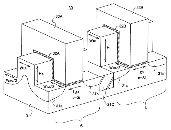
[FIRST EMBODIMENT]
FIGS.6 and 7 show the construction of a
CMOS device 30 according to a first embodiment of the
3o present invention, wherein it should be noted that
FIG.7 is a diagram showing a part of FIG.6.
Referring to FIGS.6 and 7, the CMOS device
is constructed on a Si substrate having a (100)
CA 02438214 2003-08-12
- 13 -
principal surface on which a p-type region A and an
n-type region B are formed with a separation from
each other by a device isolation region 31C. As
represented in FIG.7, the region A is formed with a
proj ection 31A having a width W1A and a height HA,
while the region B is formed with a projection 31B
having a width Wls and a height HB at both lateral
sidewalls. As can be seen from FIG.7, the top
surfaces of the projections 31A and 31B are defined
1o by the (100) surface, while the sidewall surfaces
thereof are defined by the (110) surface.
On the Si substrate 31 of FIG.7, a silicon
oxide film is formed uniformly by using the substrate
processing apparatus 20 explained with reference to
i5 FIG.2, and polysilicon gate electrodes 33A and 33B
shown in FIG.6 are formed further thereon
respectively on the region A and on the region B. The
foregoing silicon oxide film is patterned with the
patterning of the gate electrodes 33A and 33B, and
20 thus, there is formed a gate insulation film 32A in
correspondence to the gate electrode 33A and there is
formed a gate insulation film 32B in correspondence
to the gate electrode 33B.
In the p-type region A of the CMOS device
25 30 of FIG.6, there are further formed n-type
diffusion regions 31a and 31b at both sides of the
gate electrode 33A including the projection 31A, by
conducting ion implantation of an n-type impurity
while using the gate electrode 33A as a self-
3o alignment mask. Similarly, there are formed p-type
diffusion regions 31c and 31d in the n-type region B
at both Bides of the gate electrode 33B including the
projection 31B. As a result, a p-channel MOS
CA 02438214 2003-08-12
- 14 -
transistor is formed on the region A and an n-channel
MOS transistor is formed on the region B of the
substrate 31.
In the CMOS device of FIG.6, it should be
noted that the p-channel MOS transistor has a gate
length LgA while the n-channel MOS transistor has a
gate length Lga, and the gate electrode 33A covers
the flat part of the Si substrate at respective sides
of the projection 31A with a gate width WzA/2. As a
1o result, the gate width of the gate electrode 33A on
the (100) surface including the top surface of the
projection 31A is given by WiA + WzA. On the contrary,
the gate width WA of the gate electrode 33A on the
(110) surface is given by 2HA in view of the fact
that the gate electrode 33A is formed on the both
sidewall surfaces. As a result, the current
drivability of the p-channel MOS transistor formed on
the region A is given by the equation a pi (WiA+WzA) +2 I~
pzHA, wherein I~ pi represents the hole mobility on the
(100) surface while upz represents the hole mobility
on the (110) surface. .
Similarly, the current drivability of the
n-channel MOS transistor formed on the region B is
given by the equation a ni (Wir.+WzA) +2 a nzHA, wherein l~
represents the electron mobility on the (100) surface
while ~nz represents the electron mobility on the
(110) surface.
Thus, in the CMOS device 30 of the present
embodiment, in which the p-channel MOS transistor has
3o the sidewall part also on the both sidewall surfaces,
the width and the height of the projections 31A and
31B are determined such that the current drivability
thereof balances the current drivability of the n-
CA 02438214 2003-08-12
- 15 -
channel MOS transistor and hence the relationship
~ p1 ~W1A + w2A~ 'f' ~ p2wA = ~ n1 ~wlA + w2A~ +' /~ n2wA,
wherein it should be noted that the relationship
WA=2HA~ Ws=2Ha is used.
In such a construction, in particular, it
becomes possible to balance the current drivability
of the p-channel MOS transistor and the n-channel MOS
transistor by setting the heights HA and HB of the
projections 31A and 31B while maintaining the same
device area.
It should be noted that it is not always
necessary to form the transistor on the both sidewall
surfaces but it is also possible to form the
transistor only on one sidewall surface.
In the description heretofore, it was
assumed that the gate insulation films 42A and 32B
are formed of a silicon oxide film, while the present
invention also allows formation of a silicon nitride
film for the gate insulation films 32A and 32B by
forming a mixed gas plasma of a rare gas such as an
Ar or Kr gas and an NH3 gas or a mixed gas of the
rare gas and an N2 gas and a Hz gas in the substrate
processing apparatus of FIG.2. Further, it is
possible to form a silicon oxynitride film for the
gate insulation films 32A and 32B by adding thereto
an 02 gas. In this case, a p-channel MIS transistor
and an n-channel MIS transistor are obtained instead
of the p-channel MOS transistor and the n-channel MOS
transistor.
Further, the substrate 31 is not limited to
silicon in the present embodiment. For example, it is
CA 02438214 2003-08-12
- 16 -
possible to use a Site substrate in which Si is added
with other element such as Ge.
[SECOND EMBODIMENT]
FIG.8 shows the construction of a CMOS
device 40 according to a second embodiment of the
present invention.
Referring to FIG.8, the CMOS device 40 is
formed on a Si substrate 41 having a (111) surface or
1o a (110) surface as the principal surface and includes
an n-channel MOS transistor 40A having a gate
electrode 42A extending on the Si substrate 41 in a
first orientation and a p-channel MOS transistor 40B
having a gate electrode 42B extending on the Si
substrate in a second, different orientation. At both
lateral sides of the gate electrode 40A, there are
formed n-type diffusion regions 43A and 44A.
Similarly, p-type diffusion regions 43B and 44B are
formed at both lateral sides of the gate electrode
40B .
Thereby, it should be noted that there is
formed a CMOS circuit by connecting the diffusion
region 44A and the diffusion region 43B and by
connecting the gate electrodes 42A and 42B.
In the CMOS device of such a construction,
it should be noted that the current drivability of
the p-channel MOS transistor changes with the
orientation 8 thereof with respect to the p-channel
MOS transistor. In the case of the silicon wafer of
(110) orientation, the current drivability becomes
maximum in the case the direction connecting the
source and drain regions of the transistor is
oriented in the <111> direction. In the direction
CA 02438214 2003-08-12
- 17 -
rotated by 180 , on the other hand, the current
drivability becomes minimum. Further, the current
drivability takes an intermediate value between the
maximum and the minimum at an intermediate angle. In
the case of a p-channel MOS transistor,. the ratio of
the maximum and the minimum is about 2.5. In the case
of an n-channel MOS transistor, on the other hand,
the ratio of the maximum and the minimum is about 1.4.
Thus, by optimizing the mutual orientation
1o angle 8, it becomes possible to balance the current
drivability of the n-channel MOS transistor 40A and
the p-channel MOS transistor 40B.
[THIRD EMBODIMENT]
FIG.9 shows the construction of a three-
input NAND circuit that uses the CMOS circuit of any
of the foregoing embodiments.
Referring to FIG.9, the three-input NAND
circuit includes n-channel MOS transistors Tri - Tr3
connected in series between an output line connected
to an output terminal and a ground line, while there
are connected p-channel MOS transistors Tr4 - Trs in
parallel between an output line Vo~T and a supply
voltage source Vop. Thereby, an input logic signal A
is supplied to respective gates of the MOS
transistors Trl and Tr4, while another input logic
signal B is supplied to respective gates of the MOS
transistors Tr2 and Trs. Further, an input logic
signal C is supplied to respective gates of the MOS
3o transistors Tr3 and Tr6.
In FIG.9, it should be noted that the
numerals attached to the transistors indicate the
relative device area of the respective transistors.
CA 02438214 2003-08-12
~ - 18 -
Thus, in the case the entire transistors are formed
on the (100) surface of silicon, it will be noted
that the illustrated NAND circuit has the relative
device area of 18. On the other hand, in the case the
current drivability of the p-channel MOS transistor
has been increased by three times as a result of the
construction of FIG.6 or FIG.8, the device area can
be decreased to 1/3, and the relative area of the
NAND circuit is reduced to 12. As a result of the
1o decrease of the device area, the oscillation
frequency of a ring circuit, formed by cascading the
NAND circuit for 31 times, is increased from the
conventional value of 855MHz to 879MHz for the case
in which each transistor has a gate length of 0.251~m.
[FOURTH EMBODIMENT]
FIG.10 shows the construction of a three-
input NOR circuit that uses the CMOS circuit of any
of the preceding embodiments.
Referring to FIG.10, the three-input NOR
circuit includes n-channel MOS transistors Trii - Tris
connected in parallel between an output line
connected to an output terminal and a ground line,
and p-channel MOS transistors Trl4 - Trls are
connected in series between the output line VouT and
the supply voltage source Vpn. Thereby, an input
logic signal is supplied to the respective gates of
the MOS transistors Trll and Trl4, an input logic
signal B is supplied to the respective gates of the
3o MOS transistors Trl2 and Trls, and an input logic
signal C is supplied to the respective gates of the
MOS transistors Tris and Trl4.
In FIG.10, it should be noted that the
CA 02438214 2003-08-12
- 19 -
numerals attached to respective transistors represent
the relative device area of the transistors. Thus, in
the case the entire transistors are formed on the
(100) surface silicon, the illustrated NOR circuit
has the relative device area of 30. On the other hand,
when the current drivability of the p-channel MOS
transistors Tr4 - Tr6 has increased by three times as
a result of the construction of FIG.6 or FIG.8, the
necessary device area is reduced to 1/3, and the
1o relative device area of the NOR circuit is reduced to
12. As a result of such a decrease of the device area,
the ring oscillator, formed by cascading the NOR
circuit 31 for 31 stages, shows an increase of the
oscillation frequency from the conventional value of
447MHz to 879MHz, provided that each transistor has
the gate length of 0.25I~m.
[FIFTH EMBODIMENT]
FIG.11 shows the construction of a five-
input NAND circuit that uses the CMOS circuit of any
of the preceding embodiments.
Referring to FIG.11, the 5-input NAND
circuit includes n-channel MOS transistors Tr21 -
Tr25 connected in series between an output line
connected to an output terminal and a ground line,
and p-channel MOS transistors Tr26 - Tr30 are
connected in parallel between the output line VO~T and
the supply voltage source Vop. Thereby, an input
logic signal A is supplied to the respective gates of
the MOS transistors Trzi and Tr26, an input logic
signal B is supplied to respective gates of the MOS
transistors Tr22 and Tr2~, an input logic signal C is
supplied to respective gates of the MOS transistors
CA 02438214 2003-08-12
- 20 -
Tr23 and Tr2g, an input logic signal D is supplied to
respective gates of the MOS transistors Tr2a and Tr29,
and an input logic signal E is supplied to respective
gates of the MOS transistors Tr25 and Trio.
In FIG.11, it should be noted that the
numerals attached to the respective transistors
represent the relative device area of the transistors.
Thus, in the case the entire transistors are formed
on the (100) surface of silicon; the NAND circuit has
1o a relative area of 40. On the other hand, in the
event the current drivability of the p-channel MOS
transistors Tr26 - Trio are increase by three times as
a result of the construction of FIG.6 or FIG.8, the
necessary device area is decreased to 1/3, and the
relative area of the NAND circuit is reduced to 30.
[SIXTH EMBODIMENT]
FIG.12 shows the construction of a five-
input NOR circuit that uses the CMOS circuit of any
of the proceeding embodiments.
Referring to FIG.12, the five-input NOR
circuit includes n-channel MOS transistors Tr41 -
Tr45 connected parallel between an output line
connected to an output terminal and a ground line,
and p-channel MOS transistors Tr4s - Trso are
connected in series between the output line Vo~T and a
supply voltage source VDO. Thereby, an input logic
signal A is supplied to respective gates of the MOS
transistors Tr4i and Tr46, an input logic signal B is
3o supplied to the respective gates of the transistors
Tr42 and Tr4~, an input logic signal C is supplied to
the respective gates of the transistors Tr43 and Tr48,
an input logic signal D is supplied to the respective
CA 02438214 2003-08-12
- 21 -
gates of the transistors Tr44 and Tr49, and an input
logic signal E is supplied to the respective gates of
the transistors Tr4s and Trso .
It should be noted that the numerals
attached to the transistors of FIG.12 indicate the
relative device area of the respective transistors.
Thus, in the event the entire transistors are formed
on the (100) surface of silicon, the NOR circuit has
an overall relative area of 80. In the case the
1o current drivability of the p-channel MOS transistors
Tr46 - Trso has increased three times as a result of
the construction of FIG.6 or FIG.8, the necessary
device are is decreased to 1/3, and the relative area
of the NOR circuit is reduced to 30. As a result of
such a decrease of the device area, the ring
oscillator, formed by cascading the NOR circuit for
31 stages shows an increase of the oscillation
frequency from the conventional value of 207NHz to
431MHz for the case each transistor ahs the gate
length of 0 . 25 a m.
[SEVENTH EMBODIMENT]
FIG.13 shows the construction of a CMOS
switch according to a seventh embodiment of the
present invention.
Referring to FIG.13, the CMOS switch is
formed of a p-channel MOS transistor Trsl and an n-
channel MOS transistor Trsz connected parallel
between an input terminal VIN and an output terminal
3o VoUT, and causes sampling of the signal supplied to
the input terminal VIN in response to the clock
signals CLKp and CLKn supplied to the respective gate
electrodes.
CA 02438214 2003-08-12
- 22 -
FIG.14A shows the waveform of the clock
signals CLKp and CLKn, while FIG.14B shows the
waveform of the output signal obtained at the output
terminal VouT for the case a conventional p-channel
MOS transistor and a conventional n-channel MOS
transistor formed on the (100) surface of the silicon
substrate is used for the CMOS switch.
Referring to FIGS.14A and 14B, it can be
seen that the conduction of the n-channel MOS
i0 transistor Tr52 and the conduction of the p-channel
MOS transistor Tr51 is disconnected in response to
occurrence of transition in the clock signals CLKp
and CLKn. On the other hand, the conventional p-
channel MOS transistor Trsi has a larger parasitic
capacitance, associated with the large device area
thereof, as compared with the n-channel MOS
transistor Tr5z, and because of this, there is caused
a large drop of output voltage.
On the contrary to this, FIG.14C shows the
output waveform of the CMOS switch that uses the CMOS
device of the present invention. In this case, the
parasitic capacitance Cp of the p-channel MOS
transistor Trsl is reduced to the value comparable to
the parasitic capacitance Cn of the n-channel MOS
transistor Trsz, and the offset of the output voltage
is decreased significantly.
Thus, by using the CMOS device of the
present invention, a CMOS switch having an excellent
response speed is realized.
[EIGHTH EMBODIMENT]
FIG.15 shows the construction of a B-class
push-pull amplifier according to an eight embodiment
CA 02438214 2003-08-12
- 23 -
of the present invention that uses a p-channel MOS
transistor Tr61 and an n-channel MOS transistor Trsz.
Referring to FIG.15, the operational
characteristics and the parasitic device
characteristics are balanced in the B-class push-pull
amplifier of the present embodiment between the p-
channel MOS transistor Tr61 and the n-channel MOS
transistor Tr62, and it becomes possible to realize
amplification free from harmonic distortion over wide
1o dynamic range and frequency range.
Further, the present invention is not
limited to the embodiments described heretofore, but
various variations and modifications may be made
without departing from the scope of the invention
recited in the claims.
INDUSTRIAL APPLICABILITY
According to the present invention, it
becomes possible to balance the current drivability
of a p-channel MOS transistor and an n-channel MOS
transistor by using a crystal surface other than the
(100)-surface of silicon. Thereby, miniaturization of
the CMOS device is facilitated and the operational
speed is improved.