Note: Descriptions are shown in the official language in which they were submitted.
CA 02438341 2003-08-14
- 1 -
81785
Vertilas GmbH 449 001 P-WO
15.02.2002
Surface-emitting semiconductor laser
The invention relates to a semiconductor laser of the
surface-emitting type having an active zone with a pn
transition (pn junction).
Semiconductor lasers are in principle a semiconductor
diode operated in the direction of flow which generate
coherent light of a narrow spectral band by stimulated
emission and shine it in a directed manner. The
population inversion needed for the laser process is
achieved by an injection of current into the pn
transition. As a supporting measure the starting
material may be highly doped. In the region of the pn
transition in which the electrons and holes are adjacent
to one another in space, the induced radiant
recombination then takes place.
The optical resonator is formed, in the simplest case,
from two opposing optical mirrors at right angles to the
pn transition. In this construction emission takes place
in the plane perpendicular to the injection of current.
Alternatively, surface-emitting semiconductor laser
diodes are already known in which emission takes place
perpendicularly to the plane of the active zone. (In
English: vertical-cavity surface-emitting laser diode,
VCSEL) .
CA 02438341 2003-08-14
- 2 -
From US 5 936 266, a semiconductor laser of the surface
emitting type is known in which tunnel contact over the
entire surface is used to create a conductive transition
between the p side of the active zone and an n-doped
semiconductor layer. This means that n-doped
semiconductor layers can also be used on the p side of
the active zone, resulting in electrical series
resistances which are 10-30 times lower owing to the
10 improved electrical conductivity of n-doped
semiconductors. However, one disadvantage of tunnel
contact over the whole surface is that additional oxide
layers have to be provided for controlled guidance of the
current, which result in a complex and thermally
unfavourable structure of the semiconductor laser as a
whole.
US 6 052 398 describes a semiconductor laser of the
surface emitting type which has a structured tunnel
20 contact, the resonator being formed by two semiconductor
mirrors. The problem here is that the heat has to be
removed through one of the mirrors, which usually consist
of ternary or quaternary mixed crystals with
correspondingly poor thermal conductivity.
Alternatively, US 6 052 398 also mentions the use of a
dielectric mirror on the p side of the active zone
without mentioning any particular advantages attaching to
this alternative solution. In practice, this solution is
not used because reflective contact layers (usually gold
30 or silver) may diffuse into the adjacent semiconductor
layers, with the result that long term stability cannot
be guaranteed.
CA 02438341 2003-08-14
- 3 -
The aim of the invention is to provide a semiconductor
laser which can be operated under normal ambient
temperatures and which has stable long term
characteristics.
This problem is solved by a semiconductor laser having
the features of claim 1. Specifically, the features
according to the invention comprise a semiconductor layer
of the surface emitting type with an active zone having a
pn transition, with a first n-doped semiconductor layer
on the n-side of the active zone, with structured tunnel
contact (tunnel junction) on the p side of the active
zone which forms a conductivity transition or conductive
junction to a second n-doped semiconductor layer on the p
side of the active zone, with a structured dielectric
mirror which is applied to the second n-doped
semiconductor layer, with a contact layer with forms a
contact to the second n-doped semiconductor layer at the
20 point where the dielectric mirror is not applied, and
with a diffusion barrier between the contact layer and
the second n-doped semiconductor layer.
The solution according to the invention is based on the
25 finding that on the p side of the active zone the n-doped
semiconductor layer located thereon is sealed off from a
contact layer both by a dielectric mirror and also by a
diffusion barrier. The contact layer forms a heat sink
and thus allows effective removal of heat. Gold or
30 silver, in particular, are suitable for producing a good
heat sink. However, it has been found that components
from these layers may diffuse into the second n-doped
CA 02438341 2003-08-14
- 4 -
semiconductor layer and destroy it. The diffusion
barrier, together with the dielectric mirror, therefore
prevents components from the contact layer from diffusing
into the second n-doped semiconductor layer and, in the
5 worst case, entering the active zone and suppressing
radiant recombination therein. Thus, there is a free
choice of materials for the heat sink, in order to
achieve thermally optimised construction of a
semiconductor laser.
A process according to the invention for applying a
diffusion barrier comprises the features of claim 16,
wherein, in a first region, the diffusion barrier is
applied to the second n-doped semiconductor layer, in a
second region a dielectric mirror is applied to the
second n-doped semiconductor layer, and the contact layer
is applied at least over the diffusion barrier.
To summarise, the semiconductor laser according to the
invention has the following advantages:
- As a result of the structured tunnel contact (tunnel
junction) on the p side of the active zone the
remaining semiconductor layers on the p side of the
25 active zone may be n-doped. Because of the
substantially improved electrical conductivity of n-
doped semiconductors this results in electrical
series resistances which are approximately 10-30
times lower.
CA 02438341 2003-08-14
- 5 -
- The first n-doped semiconductor layer on the n-side
of the active zone serves as a charged carrier
inclusion layer.
5 - On the p side a highly reflective dielectric mirror
is used. A metallic covering layer may be provided
to increase reflectivity.
The heat is removed through the p side, i.e.
essentially by the tunnel contact, i.e. tunnel
junction, and the dielectric mirror, which may have
a low thermal resistance.
- Between the active area and the dielectric mirror a
thermally conductive layer (e. g. a binary InP layer)
may be used for expansion and for removal of the
heat.
- An integrated, e.g. galvanically produced, metal
heat sink which is provided over a larger area on
the p side may provide efficient heat removal. The
metal layer may simultaneously provide mechanical
stabilisation, which is particularly advantageous
when the substrate is completely removed on the n-
25 side, e.g. in order to obtain an increased jump in
the refractive index between the epitactic mirror
and air.
- The light decoupling is preferably carried out
30 through the n-side (based on the active layer), so
that the partially absorbing tunnel contact is
located on the opposite side from the light
CA 02438341 2003-08-14
- 6 -
decoupling, as a result of which higher illumination
power can be achieved.
Another inventive solution for which independent
5 protection is sought consists in the construction of the
dielectric mirror. Conventional dielectric mirrors
consist of ternary or quaternary mixed crystals with
correspondingly poor thermal conductivity. To improve
the heat conductivity US 6,052,398 proposes the use of a
10 metamorphic mirror of epitactic GaAs/AlAs. This binary
substance does indeed have better heat conductivity but
has poor lattice matching to the adjacent layers, which
means that as a result of crystal displacements only
limited long term stability is achievable.
It is therefore proposed, as an independent inventive
solution, to provide for the dielectric mirror an
alternating series of binary layers in such a way that
the binary layers on average have good lattice matching
20 to the adjacent layers. For example, the binary layers
may consist alternately of InAs and GaAs with layer
thicknesses of 3 nm in each case, so that the average
lattice spacing of the binary layers corresponds to the
adjacent semiconductor layer.
This solution may be implemented on its own or in
conjunction with the solution described above according
to claims 1 and 16.
30 Other preferred embodiments will become apparent from the
subsidiary claims. Naturally, the features recited
therein and those which will be explained hereinafter may
CA 02438341 2003-08-14
_ 7 _
be used not only in the combination specified but also in
other combinations or on their own.
According to a preferred embodiment an adhesion promoter
is provided between the diffusion barrier and the second
semiconductor layer. Preferably, the adhesion promoter
consists of a layer of titanium and the diffusion barrier
consists of a layer of platinum. In addition, to
increase the reflectivity between the dielectric mirror
10 and the contact layer, a metallic covering layer may be
provided. To simplify the production process the
metallic covering layer may be provided right the way
through between the diffusion barrier and the contact
layer. Suitable materials are gold for the metallic
covering layer and gold or silver for the contact layer.
The dielectric mirror consists, for example, of a
plurality of dielectric ~/4 pairs of layers, preferably
formed from materials with a large difference in
refractive index such as for example MgF2 and Si.
It is particularly advantageous if the dielectric mirror
has a lower heat resistance than the semiconductor
materials as this ensures a directed heat conduction.
25 For this purpose the second n-doped semiconductor layer
may consist of an InP semiconductor, for example.
According to another preferred embodiment, the contact
layer is applied sufficiently thickly to act as a heat
30 sink. Preferably, the contact layer is applied over the
whole surface and also covers the dielectric mirror. The
thickness of the contact layer may be 10 Vim, for example.
CA 02438341 2003-08-14
According to another preferred embodiment the light
decoupling takes place on the n side of the active zone.
Preferably, for this reason, the substrate is removed
from the n side of the active zone.
The invention will now be described more fully with
reference to various embodiments referring to the
accompanying drawings, wherein:
Fig. 1 shows a first embodiment of the invention,
Fig. 2 shows a second embodiment of the invention,
Fig. 3 shows a third embodiment of the invention,
Fig. 4 shows a fourth embodiment of the invention,
Fig. 5 shows a fifth embodiment of the invention,
Fig. 6 shows three process steps for preparing a
diffusion barrier according to a first
embodiment, and
25 Fig. 7 shows three process steps for preparing a
diffusion barrier according to a second
embodiment.
First of all, five embodiments of the invention will be
described with reference to Figures 1 to 5. What all the
embodiments have in common is a diffusion barrier between
the contact layer and the n-doped semiconductor layer on
CA 02438341 2003-08-14
_ g _
the p side of the active zone. The process steps for
forming the diffusion barrier will be explained with
reference to Figures 6 and 7.
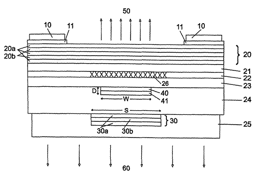
Fig. 1 shows a first embodiment of the invention. The
current is supplied through the lower p contact (25),
which simultaneously operates as an integrated heat sink,
and the n-contacts (10), which may optionally be applied
to a highly doped contact layer (11). The light escapes
10 upwards (50) while the heat is removed downwards (60)
through the integrated heat sink (25), e.g. onto a copper
housing. The active laser region (26) is situated within
the active layer (22), which preferably consists of a
braced multi-layer structure (in English: Multiquantum
well: MQW structure). The lateral dimensions of the
active laser region are determined by the flow of current
through the structured tunnel contact or tunnel junction
consisting of a highly p-doped layer (40) and a highly n-
doped layer (41) which is laterally circular in
structure, for example (diameter W), and by the lateral
expansion of the current in the layer (23) and the charge
carrier diffusion in the active layer (22). The vertical
limit of the electrons and holes injected into the active
region is provided by the n- and p-doped boundary layers
(21) and (23), respectively.
On the n side is the mirror (20) produced epitactically
according to the prior art and consisting for example of
a plurality (e.g. 36) of ~/4 pairs of layers of two
semiconductor materials (20a) and (20b) with different
refractive indices. The lower mirror (30) consists of
several (e. g. 1.5 or 2.5) pairs of dielectric ~/4 pairs
CA 02438341 2003-08-14
-
of layers (30a) and (30b), such as MgF2 (30a) and Si
(30b), for example. Its reflectivity is additionally
increased by the reflection on the lower interface with
the integrated heat sink (25), particularly if the latter
5 consists of highly reflective metals such as gold or
silver.
In the vertical direction the tunnel contact is placed in
the minimum amount of the electromagnetic field so that
10 there are no or only very negligible optical losses in
the highly doped and absorbent layers (41) and (42). For
the same reason the tunnel contact should be as thin as
possible; favourable values for the total thickness D are
to 60 nm for 1.3 to 1.55 ~m VCSEL. The second
15 semiconductor layer (24) on the p side may be (highly) n-
doped by virtue of the tunnel contact or may have a
gradient in the n doping with lower doping adjacent to
the layer (23) and higher doping on the underside towards
the mirror (30) and the integrated heat sink (25). In
20 each case there is a blocking npn structure adjacent to
the tunnel contact which blocks the flow of current at
this point so that the entire current flows through the
tunnel contact into the active layer. The layer (24)
should preferably have good thermal conductivity in order
to improve and expand the flow of heat from the active
region (e. g. to a multiple of the diameter S), thus
giving the advantage of reduced overall heating.
Thanks to the low impedance of the n-doped layer (24) the
lateral supply of current adjacent to the insulating
dielectric mirror (30) may take place without any
substantial electric losses and without generating heat.
CA 02438341 2003-08-14
- 11 -
The lateral dimension S of the dielectric mirror is
preferably selected to be at least as great as the
lateral dimension W of the tunnel contact. It is
particularly useful if the dimension S is about 3-8 ~m
5 greater than W (typically 2-20 ~m for 1.3 ~m and 1.55 ~m
VCSELs) as the lateral expansion of the optical field as
a result of the wave guiding by the amplification and
thermal lensing of the active laser region (26) is
restricted to roughly the dimension of the active laser
region.
Fig. 2 shows a second embodiment of the invention. In
contrast to Fig. 1, the manufacturing process is such
that the structure of the tunnel contact is imaged in the
15 epitactic overgrowing into the surface of the layer (24).
This results in increase lateral wave guiding which is
25
aligned precisely, in self-adjusting manner, with the
tunnel contact and the active region (26). Depending on
the course of the process, the imaging of the tunnel
contact may be widened or reduced, thus allowing the
lateral limits of the optical field to be influenced over
a wide range. This method may be combined with the
structural variants described below in order to optimise
the laser properties.
Fig. 3 shows a third embodiment of the invention. It is
clearly emphasised here that the application of an
additional highly reflective metallic layer (30c) onto
the dielectric mirror (30) as a whole can produce high
30 reflectivity which in this embodiment does not depend on
the properties of the integrated heat sink and contact
layer (25) .
CA 02438341 2003-08-14
- 12 -
Fig. 4 shows a fourth embodiment of the invention. In
this embodiment the contact resistance to the contact
layer (25) on the p side can be reduced by lateral
5 insertion of a highly n-doped intermediate contact layer
(70). For example, the layer (24) may consist of
thermally highly conductive n-doped InP and the
intermediate contact layer (70) may consist of highly n-
doped InGaAs, which produces very low contact
resistances.
As the n-doped intermediate contact layer according to
the Fig. 4 may be a poor conductor of heat, as in the
case of InGaAs, Fig. 5 shows a fifth embodiment of the
invention in which both low-impedance contact by means of
the intermediate contact layer (70) and also a good
discharge of heat through the window (71) are made
possible by the fact that an intermediate space is
provided between the dielectric mirror (30) and the
20 intermediate contact layer (70), through which the heat
is able to flow away. The lateral width of the region
(71) is therefore preferably greater than the thickness
of the layer (24).
25 Fig. 6 shows three process steps for producing a
diffusion barrier according to a first embodiment.
In a first step (a) a diffusion barrier 601 is applied to
a first area, while a second area 602 is masked. The
30 diffusion barrier may consist of platinum (Pt), for
example. In order to achieve better adhesion to the
underlying n-doped semiconductor layer, a layer of
CA 02438341 2003-08-14
- 13 -
titanium may be applied underneath the layer of platinum.
Finally, a layer of gold may be applied to the layer of
platinum. In this form the diffusion barrier then
consists of layers of Ti/Pt/Au.
In a second step (b) a dielectric mirror 603 is applied
in the second region 602. A certain overlap with the
diffusion barrier 601 may be allowed at the points 605,
606. The advantage of this overlap is that a tight seal
can be guaranteed between the dielectric mirror and the
diffusion barrier so as to safely rule out any
possibility of diffusion from the contact layer into the
n-doped semiconductor layer.
15 Finally, in a third step (c), a layer of gold 604 is
applied to the dielectric mirror 603.
Fig. 7 shows three process steps for the preparation of a
diffusion barrier according to a second embodiment. The
20 main difference from the process steps according to Fig.
6 is that, in a first process step (a), first of all a
dielectric mirror is applied and in a second process step
(b) the diffusion barrier 702 is then applied which may
in turn consist of the sequence of layers Ti/Pt/Au
25 mentioned above. Then, in a third step (c), a layer of
gold 703 is applied to the dielectric mirror. In the
process sequence according to Fig. 7 the masking must be
precisely adjusted so as to prevent diffusion between the
dielectric mirror and the n-doped semiconductor layer
30 underneath it, as before.
CA 02438341 2003-08-14
- 14 -
Table 1, finally, lists some typical data for a
semiconductor diode according to the invention, the
numbers in the first column referring to the reference
numerals in the figures.
5
CA 02438341 2003-08-14
- 7.5 -
Table 1: Typical data for a semiconductor diode according to
the invention with a wavelength of 1.55 Vim. 7:,g indicates the
wavelength corresponding to the band spacing.
No. Material Doping Thickness Diameter Note
(ClLI (ntll)
3)
10 Ti: lOnm ca. 530 55 on the
Pt: 20nm inside
Au: 500nm 240 on
the
outside
11 InGaAa (lattice n=5x10" 100 50 on the
matched to
InP) inside
250 on
the
outside
20 20a InGaAlAs (refractiven=2x10' 111 250
index
approx 3.48)
20b InAlAa (refractiven=2x10' 121 250 Repeated
index
approx 3.2) 36 times
21 InAlAS n=5x10 50 250
22 InGaAlAs (7.~=1.1)xm)Undoped 108 250
: 20nm
InGaAlAa (~=1.78m):
Snrn
InGaAlAs (7~=l.l~m):
7nm
InGaAlAs (~=1.7~m):
8nm
InGaAlAS (71,9=1
. 18m) : 7nm
InGaAlAs (~9=l.7wm):
Bnm
InGaAlAs (R9=l.lwm):
7nm
InGaAlAs (7.,9=l.7wm):
8nm
InGaAlAS (7~=l.lwm):
7nm
InGaAlAa (T9=1.7~m);
8nm
InGaAlAS (~=1.1~m):
20nm
23 InAlAa p=5x10 50 250
24 InP n=1-5x10
25 Ti: lOnm
ca. 50 250
~m
Pt: 20nm
Au : 5 0 ~xm
30 30 MgFs 280 12 2x
a
30 Si 110 12 lx
b
40 InGaAlAa (7.,9=1.4~m)p=10 20 8
41 InGaAs (lattice n=10'" 20 8
matched to
InP)
50 Light exit aperture ca. 50
~m
60 Discharge of heat ca. 250
yam