Note: Descriptions are shown in the official language in which they were submitted.
CA 02438609 2003-08-18
WO 02/073858 PCT/US02/06884
-1-
OPTICALLY AMPLIFIED BACK-UP RECEIVER
Field of the Invention
This invention relates to the field of optical
communication systems, and more particularly, this
invention relates to an optical communication system using
wavelength division multiplexed (G~1DM) optical
communication signals and having back-up receiver
capability.
Background of the Invention
G~lavelength division multiplexing (TnIDM) is commonly
used in optical communication systems for increasing the
bandwidth of a fiber optic telecommunications link,
without increasing the speed of associated electronics.
In many prior art optical communication techniques, the
bandwidth of a single channel (or wavelength fiber optic
telecommunication link) has been limited primarily by the
high-speed electronics required at the transmitter and
receiver. By using wavelength division multiplexing at a
telecommunications system receiver, the optical channels
that receive the optical communication signals are
separated, or demultiplexed, and sent to individual
receivers, which vary in their rate of data receipt. One
example of a receiver is a 2.488 Gb/S receiver.
The number of individual receivers used in the
optical communications system can vary. These
communication receivers connect into a back plane of
existing telecommunications equipment. For example, a
telecommunications rack could include one~or more
receivers, such as 8 or 16 receivers, each mounted on a
board within the telecommunications rack. when optical
components fail, it is necessary to determine the channel
CA 02438609 2003-08-18
WO 02/073858 PCT/US02/06884
-2-
that is being used by the failed optical component or
particular receiver.
In the past, telecommunication links have rerouted
signals on the electrical switching level when any optical
components failed, thus loading another path onto the
network. It would be more advantageous to re-route an
optical communication signal on a particular wavelength
channel at the receiver terminal, in the case of a
receiver failure or other optical component failure, and
not consume network bandwidth as in prior art techniques.
This would allow receiver maintenance at any time without
increasing. downtime or network re-routing.
It would also be desirable to monitor a channel and
allow continuous sweeping of the optical communications
channels. For example, if a channel showed any signs of
weakening or failure, it would be advantageous to identify
the source of the problem so that corrective measures
could be sought. Thus, there is a need for greater
channel monitoring capability. Although there are some
channel monitoring devices that use single mode fiber,
such as one commercially available system manufactured
under the trade designation "Spectra SPAN," it has no
capability as a back-up signal receiver.
Summary of the Invention
The present invention is advantageous and allows the
re-routing of optical communication signals at the
receiver terminal, in case of receiver failure or other
optical component failure. The system also does not
consume network bandwidth as in past practices, where
signals have been re-routed on the electrical switching
level when optical components failed. Thus, in the
present invention, another path is not loaded onto the
network and bandwidth is not consumed. The present
CA 02438609 2003-08-18
WO 02/073858 PCT/US02/06884
-3-
invention also allows receiver maintenance at any time,
without down time or network re-routing.
The present invention can also function as a channel
monitor, allowing continuous sweeping of optical
communication channels for quality and performance. When
a channel shows signs of weakening or failure,
identification of the source of the problem can be
triggered, and corrective measures sought. If any one of
the dedicated telecommunications system receivers fail on
any given wavelength, the back-up receiver system of the
present invention can be tuned to that particular
wavelength and take over the link, while repairs are being
conducted.
The present invention can also be used as a tracking
filter for systems that use a tunable laser for laser
transmitters that fail. The receiver can track to a new
wavelength location where a tunable transmitter has been
positioned to account for a failing, or a failed laser
transmitter. The present invention can also be used as a
tunable receiver for systems/locations requiring
tunability, such as add/drop nodes on a fiber.
In accordance with the present invention, an
optically amplified back-up receiver system includes an
optical splitter positioned along an optical
communications path for receiving a wavelength division
multiplexed (WDM) optical communications signal and
splitting a portion of the WDM optical communications
signal into a low power WDM signal onto a back-up path. An
optical amplifier receives the low power WDM signal and
amplifies same. A tunable filter receives the WDM signal
after amplification and selects an optical signal of a
desired wavelength that is to be backed-up from the
communications path. A receiver section is operatively
connected to the tunable filter and receives the selected
CA 02438609 2003-08-18
WO 02/073858 PCT/US02/06884
optical signal and backs up the desired wavelength from
the optical communications path. A receiver includes a
PIN detector for receiving the optical signal and converts
the optical signal into an electrical communications
signal.
In one aspect of the present invention, the tunable
filter comprises a fiber Fabry Perot filter. The tunable
filter also includes a controller operatively connected to
the tunable filter in a controller feedback path for
controlling the selection of desired wavelengths. An
optical/electrical converter, analog/digital converter,
and an optical coupler are operatively connected to the
tunable filter and controller and convert the optical
signals coupled from the optical coupler into digital
format for operation within the controller. A
digital/analog converter is operatively connected to the
controller and tunable filter and receives the control
signals from the controller and converts the control
signals into the analog signals directed to the tunable
filter.
In yet another aspect of the present invention, the
optical amplifier includes an injection laser diode and
current source control loop circuit connected to the
injection, laser diode that establishes a fixed current
through the injection laser diode. A voltage switcher
circuit is connected to the injection laser diode and
current source control loop circuit. A voltage switcher
circuit is adapted to receive a fixed supply voltage and
convert inductively the supply voltage down to a forward
voltage for biasing the laser diode and producing an
optical fiber coupled laser~output.
In yet another aspect of the present invention, the
detector 'includes a PIN photodiode. The receiver section
includes an amplifier circuit for amplifying the
CA 02438609 2003-08-18
WO 02/073858 PCT/US02/06884
electrical communications signal and an electronic limiter
circuit for reshaping the electrical communications
signal. The amplifier circuit also includes a data
decision circuit and clock recovery circuit for retiming
the electrical communications signal.
Brief Description of the Drawings
'Other objects, features and advantages of the
present invention will become apparent from the detailed
description of the invention which follows, when
considered in light of the accompanying drawings in which:
FIG. 1 is a block diagram of a wavelength division
multiplexed optical communications system having a
plurality of fixed receivers and a tunable optical
receiver of the present invention positioned on the back-
up path, which are connected to the back plane of existing
telecommunications equipment.
FIG. 2 is another block diagram showing add/drop
nodes, where a tunable receiver, processing equipment, and
tunable transmitter are used.
FIG. 3 is another block diagram showing an example
of a wavelength division multiplexed optical
communications system having the optically amplified back-
up receiver of the present invention.
FIG. 4 is another block diagram similar to FIG. 3,
but showing in greater detail the optically amplified
back-up receiver of the present invention.
FIG. 5 is an enlarged block diagram of the tunable
filter of the present invention having optical channel
monitoring capability with a spectrum analyzer.
FIG. 6 is a block diagram of a low power laser diode
driver used as part of the amplifier section of the
optically amplified back-up receiver of the present
invention.
CA 02438609 2003-08-18
WO 02/073858 PCT/US02/06884
_6_
Detailed Description of the Preferred Embodiments
The present invention will now be described more
fully hereinafter with reference to the accompanying
drawings, in which preferred embodiments of the invention
are shown. This invention may, however, be embodied in
many different forms and should not be construed as
limited to the embodiments set forth herein. Rather,
these embodiments are provided so that this disclosure
will be thorough and complete, and will fully convey, the
scope of the invention to those skilled in the art. Like
numbers refer to like elements throughout.
The present invention is advantageous and allows the
re-routing of optical communication signals at the
receiver terminal, in case of receiver failure or other
optical component failure. The system also does not
consume network bandwidth as in past practices, where
signals have been re-routed on the electrical switching
level when optical components failed. Thus, in the
present invention, another path is not loaded onto the
network and bandwidth is not consumed. The present
invention also allows receiver maintenance at any time,
without down time or network re-routing.
The present invention can also function as a channel
monitor, allowing continuous sweeping of optical
communication channels for quality and performance. When
a channel shows signs of weakening or failure,
identification of the source of the problem can be
triggered, and corrective measures sought. If any one of
the dedicated telecommunications system receivers fail on
any given wavelength, the back-up receiver system of the
present invention can be tuned to that particular
wavelength and take over the link, while repairs are being
conducted.
CA 02438609 2003-08-18
WO 02/073858 PCT/US02/06884
The present invention can also be used as a tracking
filter for systems that use a tunable laser for laser
transmitters that fail. The receiver can track to a new
wavelength location where a tunable transmitter has been
positioned to account for a failing, or a failed laser
transmitter. The present invention can also be used as a
tunable receiver for systems/locations requiring
tunability, such as add/drop nodes on a fiber.
FIG. 1 illustrates an optical communication system
at 10, where a wavelength division multiplexed (WDM)
optical communications signal 12 is transmitted along
optical communications path 13. The optical
communications signal 12 passes through an optical
splitter 14, positioned along the path 13, which splits
off about 50, as a non-limiting example, of the light
power comprising the optical communications signal and as
a full spectrum of that signal into a back-up path 15.~
About 950 of the wavelength division multiplexed optical
communication signal passing along the optical
communications path continues into a~WDM circuit 16, which
includes a demultiplexer for dividing the WDM optical
communications signal into separate optical communication
signals of different wavelengths ~,1 through 7~n, and into
respective fixed (dedicated) receivers 18, such as the
illustrated fixed receiver 1, fixed receiver 2, . . .
fixed receiver n, The fixed receivers 18 connect into the
back plane 20 of existing telecommunications equipment, as
known to those skilled in the art.
The optical signal 22 is formed from the split-off
portion of the light and comprises about 50 of the
original power of the WDM optical communications signal
12. It is a low power WDM optical signal having the full
spectrum of the light from the original WDM optical
CA 02438609 2003-08-18
WO 02/073858 PCT/US02/06884
_g_
communications signal 12. The tunable, optically
amplified back-up receiver 24 of the present invention
receives the optical signal 22 and selects an optical
signal of desired wavelength for the appropriate channel
to be backed-up (~,1 through 7~n) , and converts this optical
signal of desired wavelength into an electrical
communications signal to be fed into the back plane 20.
The receiver 24 of the present invention operates as a
back-up receiver in case one of the fixed receivers 18 is
inoperable, or the optical components that carry an
optical signal of a particular wavelength are inoperable.
FIG. 2 illustrates how the tunable, optically
amplified back-up receiver 24 of the present invention can
be used in a system or location requiring tunability, such
as for respective add/drop nodes 26,28 on a
telecommunications fiber. The tunable receiver 24 is
operatively connected to telecommunications processing
equipment 32 and a tunable transmitter 34. The optical
signal of selected wavelength can be dropped and received
in the tunable receiver 24. It is converted by the
receiver 24 into the appropriate electrical communications
signal, which is then processed by appropriate signal
processing circuitry, amplifier circuitry, regeneration
circuitry and other circuitry known to those skilled in
the art. Once processed, the electrical communications
signal is passed to the tunable transmitter 34, which
converts the electrical communications signal that had
been processed into an optical signal. It is then added
to the main optical communications signal 12 passing along
the main optical communications path 13.
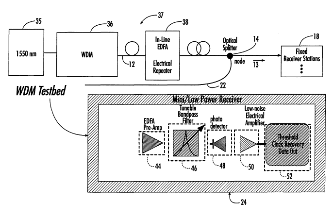
FIG. 3 illustrates a high level block diagram of the
optical communications system 10 where optical
communications signals 35 of about 1550 nanometers are
CA 02438609 2003-08-18
WO 02/073858 PCT/US02/06884
-9-
wavelength division multiplexed 36 into optical
communications signal 12 at about 155 Mb/S to about 4 Gb/S
in a high bandwidth data distribution system 37, including
appropriate in-line, erbium doped fiber amplifiers 38
acting as optical repeaters. The amplified optical
communications signal 12 is passed to the dedicated
optical receivers 18 along the main optical communications
path 13.
The optical splitter 14 forms a node that allows the
full spectrum of the wavelength division multiplexed
optical communications signal to be split off (about 50 of
its power) and passed into back-up path 15 as an optical
signal 22 and to the tunable mini/low power optically
amplified back-up receiver 24 of the present invention.
The tunable optically amplified back-up receiver 24
of the present invention includes an erbium doped fiber
amplifier 44 (EDFA) acting as a preamplifier. This
permits amplification of the low power optical signal
before passing into the tunable bandpass filter 46, which
selects one of the desired wavelengths, 7~1 through ~,n. A
photodetector, which in the present embodiment is a PIN
diode 48, but also can be an Avalanche Photo Diode (APD),
converts the amplified and optical signal of desired
wavelength into an electrical communications signal and
passes that electrical communications signal into a low-
noise electrical amplifier 50 and into the clock and data
recovery circuit 52.
FIG. 4 illustrates greater details of the tunable
optically amplified back-up receiver 24 of the present
invention, and illustrating three main sections as an
amplifier section 54, having the erbium-doped fiber
amplifier (EDFA) 44 as shown in FIG. 3, a tunable filter
CA 02438609 2003-08-18
WO 02/073858 PCT/US02/06884
-10-
section 56, and the receiver section 58 operable as a
detector used at different wavelengths. The detector
electronics is selected to support typical data rates,
including 2.5 and 10.0 Gb/S.
Although the ranges of data and number of used
channels are set forth as non-limiting examples, it should
be understood that the present invention is advantageously
used with different wavelengths and different number of
channels. As illustrated, the WDM optical communications
signal, such as 2.5 Gb/S WDM signal input, passes into a
1550/980 WDM input circuit 58a that is operable with a
Fiber Bragg Grating Stabilized Pump Laser Diode circuit 59
and a low power laser diode driver circuit 60.
Although different laser diode drivers can be used
in accordance with the present invention, in one aspect of
the present invention, the low power laser diode driver is
illustrated in FIG. 6, and can be used with the tunable
receiver of the present invention. This low power laser
driver circuit 60 can be used for driving the optical
preamplifier and receiver assembly shown in FIG. 4.
A five volt supply voltage input is standard with
many electronic circuits. The laser driver circuit 60
includes an injection laser diode 62 that is, in one
aspect of the present invention, a high quantum efficiency
injection laser diode (HQEILD). A current source control
loop circuit 64 is connected to the injection laser diode
62 and establishes a fixed current through the injection
laser diode. This current source control loop circuit 64
has a voltage switcher circuit chip 66 connected to the
injection laser diode, within the current source control
loop circuit, and is adapted to receive the fixed supply
voltage of five volts and convert inductively the supply
voltage down to a forward voltage, to bias the laser
CA 02438609 2003-08-18
WO 02/073858 PCT/US02/06884
-11-
injection diode and produce an optical output having
minimized power losses.
This voltage switcher circuit chip 66 is
monolithically formed as a single circuit chip, and is
used as a high efficiency voltage converter as shown in
FIG. 6.
The current source control loop circuit 64 includes
the high efficiency current source 70, acting as a low
noise current source and the current control circuit 72.
These circuits are all contained within one housing, and
in one aspect, on a printed circuit card assembly 74 that
includes the receiver components, including the
preamplifier, tunable bandpass filter circuit and optical-
to-electrical conversion circuit.
The schematic circuit diagram shows various power
and voltage, as well as current parameters. In this
non-limiting example, at 260 milliwatts and at five volts
DC, there is a 35 decibel optical gain, with one channel
as a design goal. There could be a 266 milliwatt DC for
eight channels, and 220 milliwatts DC achieved. The Bragg
grating 73 is operatively connected to the injection laser
diode 62, and is operative by principles known to those
skilled in the art. The Bragg grating 73 is configured
for receiving the optical output and stabilizing the
optical wavelength.
As shown in FIG. 4, an ASE Reduction Stage circuit
80 works in conjunction with an isolator circuit 82 using
amplification techniques known to those skilled in the
art. The tunable filter section 56 includes the tunable
filter 46, which in one aspect of the present invention,
is a fiber Fabry Perot tunable filter 84. A 1:99 coupler
88, as a non-limiting example, allows a portion of the
optical signal to be converted by a photodetector to an
CA 02438609 2003-08-18
WO 02/073858 PCT/US02/06884
-12-
electrical current, and pass into a feedback control
circuit 87, including an analog/digital converter 88, a
low power controller 90, which is operative with a
controller interface 92 and associated electronics, and
digital/analog converter 94, for converting digitally
processed control signals back to analog control signals
and selectively tuning the fiber Fabry Perot tunable
filter. This circuitry also allows an optical spectrum to
be detected and stored.
The optical communications signal, once tuned to the
desired wavelength and frequency, passes into the receiver
section 58 that includes an optical-to-electrical
conversion circuit having the detector, i.e., the PIN
photodiode 48, followed by the low noise electrical
amplifier 50, which in one aspect of the invention, is a
preferred transimpedance amplifier and amplifies the
converted electrical communication signal received from
PIN photodiode 48. An electronic limiter circuit 96
receives the electrical communications signal and works in
conjunction with a clock and data recovery circuit 52.
This circuit allows data recovery and reshaping of
electrical communication signals. A clock recovery
circuit portion of circuit 52 allows recovery of clock
signals and retiming of electrical communication signals
by techniques known to those skilled in the art.
The data is output to the back plane 20 as shown in
FIG. 1. In the embodiment shown in FIG. 2, the signal is
sent to the processing equipment 32, and tunable
transmitter 34, which then passes the signal back onto the
main optical communication path 13.
In one non-limiting example of the present
invention, the amplifier section 54 has about 230 mW with
commercial off the shelf components (COTS) of about 2.0
CA 02438609 2003-08-18
WO 02/073858 PCT/US02/06884
-13-
watts, followed by the tunable filter section 56 operable
at about 50 mW and COTS of about 6 W, and the receiver
section 58 of about 680 mW and COTS of 1.5 W for a 2.5
Gb/S data rate.
The optical sensitivity at 2.5 Gb/S can be less than
about -40 dBm at 1 x 10⁻¹° BER (bit error rate) with a
total one channel power consumption of about 960 mW. For
a non-limiting example of eight channels, it is possible
to use a fixed ~, demultiplexer providing a total power
consumption of about 5.7 W, corresponding to 710
mW/channel.
Referring now to FIG. 5, there is illustrated the
tunable filter that has been modified to have channel
monitoring or optical spectrum analysis capability in
accordance with another aspect of the present invention.
Between the analog/digital conversion circuit 88 and the
low power controller 90, an optical channel monitoring
circuit 100 is connected. The circuit 100 can include a
spectrum analyzer, power meter or other associated
electronic equipment for monitoring the channel. Thus, it
is possible to select various wavelengths to monitor the
operation of the particular channel and determine if there
are errors in data transmission or other selected aspects.
In this aspect of the invention, the tunable filter can
be swept and the optical power stored in a processor
memory, controller or other means known to those skilled
in the art. This data can be processed and subsequently
displayed, providing an optical spectrum analysis of the
signal. The system can.monitor averaged power and
supervisory communications data. It also can perform an
optical spectrum analysis of the signals.
It is also possible to use the optically amplified
back-up receiver as a tracking filter for systems that use
CA 02438609 2003-08-18
WO 02/073858 PCT/US02/06884
-z4-
the tunable laser for laser transmitters that fail. The
receiver can track to a new wavelength location where the
tunable transmitter has been positioned to account for
failing or failed laser transmitter.
This application is related to copending patent
application entitled, "WDM CHANNEL MONITORING SYSTEM AND
METHOD," which is filed on the same date and by the same
assignee and inventors, the disclosure which is hereby
incorporated by reference.
Many modifications and other embodiments of the
invention will come to the mind of one skilled in the art
having the benefit of the teachings presented in the
foregoing descriptions and the associated drawings.
Therefore, it is to be understood that the invention is
not to be limited to the specific embodiments disclosed,
and that the modifications and embodiments are intended to
be included within the scope of the dependent claims.