Note: Descriptions are shown in the official language in which they were submitted.
CA 02438871 2003-08-19
WO 02/073527 PCT/US02/07356
SOLID-STATE QUANTUM DOT DEVICES AND QUANTUM
COMPUTING USING NANOSTRUCTURED LOGIC GATES
FIELD OF THE INVENTION
[0001] This invention pertains generally to the field of semiconductor
devices and to quantum computing carried out in semiconductor devices.
BACKGROUND OF THE INVENTION
[0002] Quantum computing utilizes quantum particles to carry out
computational processes. The fundamental unit of quantum information is called
a
quantum bit or qubit. A qubit can be both a zero and a one at the same time.
An
example is the spin of an electron, wherein the up or down spin can correspond
to a
zero, a one, or a superposition of states in which it is both up and down at
the same
time. Performing a calculation using the electron essentially performs the
operation
simultaneously for both a zero and a one. Experimental advances in quantum
computation have come most rapidly in nuclear magnetic resonance (NMR) and ion-
trap systems. The success of few-qubit quantum computation in such systems
demonstrates an urgent need for a quantum computing scheme that is scaleable
to a
large number of qubits. Solid-state qubits are one of the primary candidates.
Numerous proposals have been made for solid-state quantum computers. These
proposals include the use of nuclear spins as qubits, B.E. Kane, "A Silicon-
Based
Nuclear Spin Quantum Computer," Nature, Vol. 393 (6681), 1998, pp. 133-137;
and the use of electronic spins as quantum dots, DiVincenzo, et al., "Quantum
Computers and Quantum Coherence," J. of Magnetism and Magnetic Materials,
Vol. 200, (1-3), 1999, pp. 202-218. Potential issues with such proposed
systems
include individual impurity spins, as well as gate operation and readout
methods for
the quantum dots.
[0003] Spins can be manipulated using a strong DC magnetic field combined
with a spatially uniform radio frequency (i.e., at GHz frequencies) field. In
the
CA 02438871 2003-08-19
WO 02/073527 PCT/US02/07356
-2-
presence of a small g-factor gradient, the spins can be addressed
individually.
Entanglement of one spin with another proceeds by gating the barrier between
spins.
This gives rise to a time-dependent exchange interaction, H(t)=J(t)S,~S2. A
combination of these operations acting in the proper sequence on two qubits
will
produce a controlled-NOT gate (C-NOT). See, e.g., R. Vrijen, et al., "Electron-
Spin Resonance Transistors for Quantum Computing and Silicon-Germanium
Heterostructures," Physical Review A (Atomic, Molecular, and Optical Physics),
Vol. 62 (1), 2000, pp. 012306/1-10.
[0004] Quantum computation also can be performed without g-factor tuning
and the individual spin rotations via high frequency radiation that g-factor
tuning
allows. Instead, the time-dependent exchange interaction, H(t)=J(t)S1~S2, can
be
used in combination with coded qubits, D.P. DiVincenzo, D. Bacon, J. Kempe, G.
Burkard, K.B. Whaley, Nature (London) 408, 339 (2000), in which a single qubit
is represented by the total wavefunction of several individual spins. In this
way, the
exchange interaction alone enables universal quantum computation.
SUMMARY OF THE INVENTION
[0005] In accordance with the present invention, electron quantum dot
semiconductor devices may be utilized for such purposes as quantum computing,
quantum memory, and quantum information processing. The invention may be
implemented in a semiconductor heterostructure to trap individual electrons in
a
solid, bring these electrons close to each other, maintain phase coherence of
the
electrons, and allow individual rotation of the spin of the electrons.
[0006] A semiconductor quantum dot device in accordance with the
invention includes a multiple layer semiconductor structure having a quantum
well,
a back gate electrode, and a plurality of spaced surface electrode gates. The
electrode gates are spaced from each other by a region beneath which quantum
dots
may be defined. A tunnel barrier layer is provided between the back gate and
the
quantum well, and a barrier layer is formed over the quantum well layer.
CA 02438871 2003-08-19
WO 02/073527 PCT/US02/07356
-3-
Appropriate voltages applied to the electrodes allow the development and
appropriate positioning of the quantum dots. This arrangement in accordance
with
the invention allows a large number of quantum dots, each containing as few as
one
electron, to be formed in a series with appropriate coupling between the
quantum
dots, enabling quantum computation with a large number of qubits. In addition
to
the embodiment of the present invention in a quantum computer, the invention
may
also be implemented in other applications such as a single electron transistor
and in
integrated circuit technologies where control of one or a few electrons is
desired.
[0007] The heterostructure and split top gates that enable the creation of
coupled quantum dots may also be used to channel electrons across an
integrated
circuit. In this mode of operation, the invention provides a local tuning of
the
potential in a quantum well to provide channels in which individual electrons
can be
moved through a series of devices enabling, for example, readout of quantum
memory.
[0008] Further objects, features and advantages of the invention will be
apparent from the following~detailed description when taken in conjunction
with the
accompanying drawings.
BRIEF DESCRIPTION OF THE DRAWINGS
[0009] In the drawings:
[0010] Fig. 1 is a partial plan view of a quantum dot semiconductor device
in accordance with the present invention.
[0011] Fig. 2 is a simplified cross-sectional view of an exemplary Site
based semiconductor device of the type shown in Fig. 1 taken generally along
the
lines 2-2 of Fig. 1.
CA 02438871 2003-08-19
WO 02/073527 PCT/US02/07356
-4-
[0012] Fig. 3 is a simplified cross-sectional view of another exemplary Site
semiconductor device of the type shown in Fig. 1 taken generally along the
lines 2-2
of Fig. 1.
[0013] Fig. 4 is a simplified cross-sectional view of an exemplary
GaAs\AIGaAs based semiconductor device of the type shown in Fig. 1 taken
generally along the lines 2-2 of Fig. 1.
[0014] Fig. 5 is a schematic circuit diagram of a charge sensor connected to
a quantum dot.
[0015] Fig. 6 is a diagram illustrating the manner in which qubits can be
fabricated side-by-side to allow scaling up of a quantum computer to a large
number
of qubits.
[0016] Fig. 7 are timing diagrams showing the time sequence for the
operation of a C-NOT gate implemented utilizing the invention.
[0017] Fig. 8 are timing diagrams showing the detailed gate-voltage
sequence for the operation of the protocol for readout of the qubit state in
accordance with the invention.
[0018] Fig. 9 is a simplified perspective view of a quantum dot
semiconductor device in accordance with the invention.
[0019] Fig. 10 is a plan view of a multiple quantum dot device having the
structure of Fig. 9.
[0020] Fig. 11 is a graph showing the exchange coupling J, computed for a
simplified quantum dot device of the type shown in Fig. 9, as a function of
top gate
potentials Vo~~ and V;~.
[0021] Fig. 12 is a computed map of electrostatic potential for the device of
Fig. 9 at the point A of Fig. 11, computed at the middle of the quantum well.
CA 02438871 2003-08-19
WO 02/073527 PCT/US02/07356
-S-
[0022] Fig. 13 is a computed map of charge density for the device of Fig. 9
at the point A of Fig. 11, computed at the middle of the quantum well.
[0023] Fig. 14 is a computed map of electrostatic potential for the device of
Fig. 9 at the point B of the Fig. 11, computed at the middle of the quantum
well.
[0024] Fig. 15 is a computed map of charge density for the device of Fig. 9
at the point B of Fig. 11, computed at the middle of the quantum well.
[0025] Fig. 16 is a graph showing the excitation energy for changing the
quantum dot occupation number computed for the device of Fig. 9 for a range of
gate potentials V;~ arid Vo"
[0026] Fig. 17 are graphs showing step grading variations for a sequence of
growth layers for a heterostructure as in Fig. 9.
[0027] Fig. 18 are graphs showing the degree of strain relaxation with the
step grading variations of Fig. 17.
[0028] Fig. 19 is a graph showing a simplified pseudo-digital dependence of
the
exchange coupling J on the gate voltage V .
[0029] Fig. 20 is a top view of patterned control electrode gates.
[0030] Fig. 21 is a top view of another design for patterned control electrode
gates providing a bistable qubit design.
[0031] Fig. 22 is a scaled-up array of the control electrode gates of the type
shown in Fig. 21 wherein each qubit has a pseudo-digital exchange coupling J
with
its neighbors, and wherein each vertical pair of circles represents a single
qubit.
DETAILED DESCRIPTION OF THE INVENTION
[0032] The present invention enables the fabrication of single electron
quantum dots, or few electron quantum dots, in semiconductors in a manner that
CA 02438871 2003-08-19
WO 02/073527 PCT/US02/07356
-6-
will simultaneously allow coupling between many adjacent dots. The invention
provides a spin-based qubit for quantum computation, and allows the
measurement
of individual spin states in small quantum dots. The invention provides
advantages
in coupling low-occupation quantum dots, such as in quantum dot cellular
automata,
and enables coupling of multiple single electron or whole dots together to
allow
tunneling between adjacent dots.
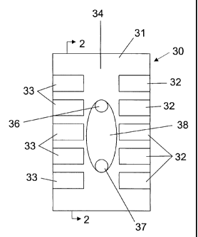
[0033] An exemplary semiconductor device providing quantum dot
interaction in accordance with the invention is shown generally at 30 in Fig.
1 and
examples of material systems for the device 30 are shown in cross-sections in
Figs.
2, 3, and 4. The device of Fig. 1 includes a semiconductor structure 31 on
which
are formed a plurality of surface electrode gates 32 and 33, i.e., at least
one gate 32
and one gate 33, which are separated from each other by an intergate region 34
as
shown in Fig. 1, multiple spaced gates 32 and 33 may be utilized to allow two
quantum dots 36 and 37 to be defined. The quantum dots 36 and 37 are separated
by a tunable coupling region 38. As shown in the cross-sectional views of
Figs. 2,
3, and 4, the semiconductor structure 31 is preferably a heterostructure that
includes
an effective substrate 40, a highly doped and conductive back gate 41, and a
tunnel
barrier 42 formed on the back gate. A first quantum well layer 44 and
optionally, a
second quantum well layer 45 are formed between the lower barrier layer 42 and
an
upper spacer or barrier layer 47 (e.g., 30 nm thick). Alternatively, the
layers 44
and 45 may be combined into a single layer 44 as shown in Figs. 3 and 4. In
this
case, the composition of the single layer (44, 45) may be chosen to maximize
spin
coherence, or to fine tune the band offsets. A capping layer 48 of, e.g., Si,
is
formed over the upper layer barrier 47, and the gates (gates 33 are shown in
Fig. 2)
formed, e.g., of gold or other metal, are deposited on the top of the capping
layer
48. As used herein, a heterostructure is a series of epitaxial layers that may
be
chosen to allow electron or hole confinement in one or more of the layers.
Epitaxial
means that that the crystal structure is not interrupted at the interface
between
layers.
CA 02438871 2003-08-19
WO 02/073527 PCT/US02/07356
_7_
[0034] Each of the layers described above in the semiconductor
heterostructure may be made of various materials. For example, the substrate,
the
back gate, and the tunnel barrier may all be made from Site. A double layer
quantum well may be made of a first layer of Site and a second layer of Ge.
Alternatively, the quantum well may be a single layer of 100 % Si in order to
maximize spin coherence, or may be made of a layer of Site in order to fine
tune
the band offsets. Finally, the capping layer may be a layer of Si. Such
embodiments are shown in Figs. 2 and 3. Alternatively, the substrate, the back
gate, and the quantum well may each be made from GaAs and the tunnel barrier
and
the upper spacer layer may be made of AIGaAs. In this configuration, a capping
layer of GaAs is formed over the upper barrier 47. Fig. 4 depicts such a
semiconductor heterostructure. Exemplary layer thicknesses and compositions
for
the multilayer heterostructures 31 are shown in Figs. 2-4 (not drawn to
scale).
These material systems are shown for purposes of illustration, and it is
understood
that other material systems may be utilized. Preferably, the spacing between
the
quantum well layer 45 and the gates 32 and 33 at the top of the
heterostructure is in
the range of about 30 to 50 nm (e.g., 33 nm as shown in Figs. 2-4), and the
preferred spacing between the gate electrodes 32 and 33, and between adjacent
electrodes 32 and adjacent electrodes 33, is in the range of about 10 nm to 50
nm.
[0035] The qubit in the device 30 is the spin of a single electron (or
possibly
several electrons) in the quantum dots 36 and 37. The heterostructure 31
provides a
Site field effect transistor (FET) structure that confines the electrons in a
direction
perpendicular to the layers and the device surface, while the gates 32 and 33
provide
lateral confinement. A readable controlled-NOT (C-NOT) gate utilizes three
such
dots in a row at a separation of about 100 nm between dots. All of the dots
may be
prepared in the "up" state by thermal relaxation in a field. The first dot 36
may be
the control dot (DOT 1) and the second dot 37 may be the target dot (DOT 2).
The
two dots may be manipulated individually utilizing GHz pulses. When the
barrier
between the two dots is partially lowered, the spin-spin interaction,
H(t)=J(t)S,~SZ
(S, is the spin of a DOT 1 and SZ is a spin of DOT 2) is tuned so that J(t)
can be
CA 02438871 2003-08-19
WO 02/073527 PCT/US02/07356
_g_
chosen. This interaction entangles the spins of the two dots. J(t) can then be
controlled, as well as a single qubit operation, to allow performance of a set
of
operations including the universal controlled-NOT gate. A third dot (DOT 3,
not
shown in Fig. 1) functions as the readout dot. If the barrier between DOT 1
and
DOT 3 is lowered (by a relatively large amount), tunneling can be induced from
DOT 2 to DOT 3. A measurement of the energy required to induce the tunneling
determines whether DOT 2 was in a spin-up or spin-down state. This measurement
is "strong" in the sense that it is sufficient to allow a final readout of a
quantum
computation. This arrangement can be scaled up to a large number of dots
(e.g.,
tens, hundreds or more) utilizing standard lithography techniques.
[0036] For clarification, it is noted that the term "gates" is used herein to
refer to different types of structures. The surface gates 32 and 33 are metal
films on
the semiconductor surface which act like the gate of a field effect
transistor. The
surface gates can be patterned on very small scales, e.g., lateral dimension
of 40 nm
or less. The back gate 41 is a doped layer below the quantum dots, and acts as
a
metallic (highly conductive) plane for the purpose of electrostatically
defining the
dots. It is also the source of the electrons or holes in the dots. Both the
surface
gates and the back gates are physical entities. A quantum gate is an operation
that is
applied to the quantum bits (qubits). The quantum gate refers to these
operations
and can apply to the physical series of voltage pulses applied to one qubit to
achieve
the effect of a quantum gate. An example of a quantum gate is the controlled-
NOT
gate, or C-NOT gate.
[0037] The present invention has several advantages. Unlike some prior
solid-state designs, the invention does not utilize impurities to bind
individual
electrons as qubits. Instead, it employs a new type of quantum dot that is
optimized
for single electron occupation. This is significant because it is not
necessary to
align gates to impurities at unknown locations, which is difficult to do in
practice
and would require unproven fabrication techniques. In addition, each qubit is
a hole
or electron trapped in a potential well, with the well formed vertically by
means of
CA 02438871 2003-08-19
WO 02/073527 PCT/US02/07356
-9-
band-edge engineering and laterally by electrostatic gates. In the present
invention,
a tunnel-coupled back gate (41) is incorporated into the semiconductor
structure (31)
that enables tuning of the number of carriers on the dot without regard to the
lateral
distance to the next nearest dot or lateral electron reservoir, thereby
enabling robust
few or single electron quantum dots (artificial impurities). Further, the
invention
preferably utilizes depletion gates (the gates 32 and 33) to define the qubit.
These
depletion gates cover a continuous conducting layer that is only subsequently
pushed
back through the back gate to reveal the final qubit. The symmetry of the
present
design also allows shifting of the qubit laterally by adjusting the position
of each
qubit's confinement well, enabling control of the Coulomb exchange coupling
between qubits.
[0038] The invention can be implemented in any semiconductor
heterostructure in which band structure engineering can be performed by
composition or strain manipulation of the band gap in a sequence of layers.
[0039] The present invention meets the requirements for a successful solid-
state quantum computing device because of its ability to manipulate and
measure
individual qubits. The manipulation and measurement are sensitive enough to
detect
individual qubits, are localized sufficiently to allow manipulation of
neighboring
qubits with negligible cross-contamination, and are fast compared with the
decoherence time for individual qubits so that error correction can be
efficient.
[0040] The state of the qubit is the state of a single spin in a solid-state
environment. Detection of such spins by their magnetic moment alone is not
currently practical. In the present invention, detection of individual charges
can be
carried out utilizing low-noise field effect transistors or single electron
transistors,
both of which have enough sensitivity to detect individual electron charges.
Field
effect transistors (FETs) are a natural choice for large-scale manufacturing.
Single
electron transistors are actually easier to fabricate for research because
they can be
fabricated in a single lithographic step.
CA 02438871 2003-08-19
WO 02/073527 PCT/US02/07356
-10-
[0041] Manipulation of solid-state spin qubits can proceed via two protocols.
Single quantum dot qubit quantum computing involves two processes: the
rotation
of individual spins, and the coupling of adjacent spins via the exchange
Coulomb
interaction for specific periods of time at a known interaction strength.
Coded qubit
quantum computing uses several quantum dots to represent a single qubit, with
the
advantage that only the exchange Coulomb interaction is required, and single
spin
rotation is not required.
[0042] Manipulation of individual spins can be accomplished by tuning the
g-factor of each spin, for example, by exploiting the different g-factors for
electrons
in Si (g~2) and in Ge (g~1.6). In the qubit device 30 of Fig. 2, electrons are
confined in a silicon quantum well 44-45, with relaxed Site confinement
barriers 42
and 47. It is possible to add a small vertical gradient of Ge in the mostly Si
quantum well. Small changes in gate voltage which are insufficient to change
the
electron population of the qubit will nonetheless enable sufficient tuning of
the
electron g-factor to move its electron spin resonance line with respect to all
of the
other qubits. Coupling between adjacent qubits can be adjusted by controlling
the
position of the qubit, which is adjustable on the length scale of the inter-
qubit
spacing 38, and by tuning the barrier height between qubits. Such operations
are
made possible by the series of spaced gates 32 and 33 that define the qubit.
Such
flexibility for defining the quantum dot is a significant advantage of the
present
invention. Control of the exchange interaction requires characterization of
each
qubit, a process that can be automated under computer control to scale to
large
numbers of qubits.
[0043] The voltage manipulations and measurements must be performed at
times which are relatively small compared to the decoherence times, which may
be
as large as seconds at low temperature. Practical computations require speeds
that
may be a million times faster than the decoherence times, such that localized
electronics may be operated at MHz rates or higher. To operate the system at
higher temperatures reduces the decoherence times, requiring faster control.
CA 02438871 2003-08-19
WO 02/073527 PCT/US02/07356
-11-
[0044] The following is an exemplary fabrication process for the quantum
dot device 30 illustrated in Figs. 1 and 2. It is understood that this process
is
exemplary only, and many variations are possible, for example, by the use of x-
ray
lithography or photolithography rather than the use of e-beam writing, by the
use of
a wide variety of etches, and so forth.
[0045] The first step is the growth of a semiconductor heterostructure 31
which confines a two-dimensional electron or hole layer in a quantum well
located
just above a back gate 41 and close enough to the back gate to allow tunneling
between the back gate and the quantum well 44, 45. The quantum well may
contain
a gradient in composition to allow tuning of the g-factor by application of an
applied
voltage to the top gates 32 and 33.
[0046] A contact is formed to the back gate 41 without contacting the
carriers in the quantum well. This may be accomplished by etching a region on
the
semiconductor chip structure, for example, by using photolithography followed
by
reactive ion etching or wet etches to a depth below the back gate 41, followed
by
forming an ohmic contact to the back gate.
[0047] Electron beam lithography may then be utilized to pattern an array of
gates 32 and 33 as shown in Fig. 1. The gates may be fabricated by metal
deposition and lift-off in a conventional manner.
[0048] The device 30 functions by applying selected voltages to the
individual surface gates 32 and 33 with respect to the back gate 41.
Electrostatic
repulsion will cause carriers (holes or electrons) to be removed from the
quantum
well 44, 45 beneath the surface gates and in the surrounding areas. One or a
few
carriers will be left in the exposed regions 34 between the gates 32 and 33.
These
isolated areas become the quantum dots.
[0049] To allow readout from the device, a charge sensor 55 including a
FET 56 may be connected as shown in Fig. 3, wherein selected voltages are
applied
to an electrode gate (e.g., one of the gates 32) from a source 57 which may
include
CA 02438871 2003-08-19
WO 02/073527 PCT/US02/07356
-12-
AC and DC voltage supplies as shown in Fig. 5. Preferably, selected voltages
can
be applied individually to each of the gates 32 and 33. A selected voltage is
applied
to the back gate 41 from a source 58, with a bias voltage being provided from
a bias
voltage supply 59 to the back gate. The purpose of the charge sensor 55 is to
monitor the charge in the quantum dot and detect changes in charge. The
circuit is
an AC bridge which is balanced when no tunneling occurs to the dot, and the
FET
56 then records no signal. When the gate voltage is adjusted to allow
tunneling,
excess charge flows from the back gate, and a signal charge is recorded on the
FET.
In small scale operation, the charge sensor can be a commercial field effect
transistor 56 having its gate electrically connected to the gate 32 by a short
wire.
The FET can be attached to the back gate 41 in the case of a single quantum
dot, as
shown in Fig. 5, but would be attached to a top gate 32 or 33 adjacent to the
dot of
interest in the case of many dots coupled in a linear array.
[0050] An advantage of the present invention is its scalability. The foregoing
fabrication steps do not limit the number of dots that may be fabricated in
series, as
illustrated by the multiple linearly aligned quantum dots 60 shown in Fig. 6.
Although a linear coupling is shown, the chain of dots 60 can be curved to
allow
dense packing on a semiconductor chip. The gates 32 and 33 between dots allow
tunable coupling which is necessary to produce the quantum gate operations.
For a
large scale operation, field effect transistors may be fabricated by standard
silicon
processing techniques and connected to the array of gates defining the dot.
One
FET per dot may be used to allow readout of the charge state of each dot. In
every
case, a single electron transistor can be utilized rather than a field-effect
transistor.
[0051] The foregoing device is preferably formed to function at temperatures
below 4.2 Kelvins, because of the increase in the spin coherence time at such
temperatures.
[0052] It is noted that each quantum dot will be different from its neighbors
and from every other dot, because of disorder in the semiconductor structure.
For
this reason, a computer may be utilized to characterize each qubit and to
determine
CA 02438871 2003-08-19
WO 02/073527 PCT/US02/07356
-13-
the voltages to be applied to each gate 32 and 33 to define the dots.
Operations are
performed by varying the voltages on the gates to control the exchange
coupling
between electrons or holes in adjacent dots, permitting universal quantum
computation. In addition to the coupling between adjacent dots, single spin
rotations
may be achieved by tuning the g-factor of electrons to allow a radio frequency
field
to rotate each spin individually but coherently. This feature is not required
in the
coded qubit mode of operation.
[0053] As noted above, construction of a readable control-NOT (C-NOT)
gate uses three quantum dots in a row at a separation of about 100 nm between
dots.
All dots may be prepared in the "up" state by thermal relaxation in a field,
where
the first dot (Dot 1) is the control dot, the second dot (Dot 2) is the target
dot, and
the third dot (Dot 3) is the readout dot. Dots 1 and 2 can be manipulated
individually by voltage pulses. When the barrier between Dots 1 and 2 is
partially
lowered, the spin-spin interaction is turned on such that J(t) can be chosen,
which
interaction entangles the spins of Dots 1 and 2. J(t), as well as the single
bit qubit
operation, is controlled to allow a desired set of operations, including the
universal
C-NOT gate. If the barrier between Dots 2 and 3 is lowered (by a relatively
large
amount), tunneling can be induced from Dot 2 to Dot 3. A measurement of the
energy required to induce the tunneling determines whether Dot 2 was spin-up
or
spin-down. This measurement is "strong." The three dots are sufficient for
construction of a C-NOT gate which can have a basic operation as follows. The
three dots are allowed to relax in a DC magnetic field of 2-5 T perpendicular
to the
semiconductor wafer for a time which is long compared to the environmental
decoherence time, which is estimated to be in the range of 1 second to 1
millisecond. The three spins of the three dots are all in the "up" state at
that point.
The system is then bathed in a field Ho operating at about 50 GHz. Spin 1 is
shifted
electrostatically into a Ge-rich region until its resonant frequency matches
the
applied frequency, and is then held there for a time t=h/4pBHo, and is then
brought
out of resonance, i.e., it is subjected to a ~/2 pulse. Then, a similar
operation is
carried out on spin 2. Following this, the barrier between spins 1 and 2 is
CA 02438871 2003-08-19
WO 02/073527 PCT/US02/07356
-14-
electrostatically lowered by a relatively small amount, forcing spins 1 and 2
to
interact via H(t)=J(t)S,~S2. The gate is timed such that this interaction
lasts a time
t=h/4Jo (this is for a square pulse; more generally, the time integral of J(t)
should
be h/4). This is the square root of the swap operator in which the two spin
directions are interchanged. Spin 1 is then subjected to a ~ pulse. Finally,
the
square root swap is repeated. The sequence of five operations is the complete
C-
NOT logic gate, the operation of which is illustrated schematically in Fig. 7
showing the timing sequences for the operation of the gate. Spins 1 and 2 (the
top
two lines) are subjected to rotations (the lined boxes) and mutual
interactions
(represented by the wavy lines). V1 and V2 are the voltages on gates adjacent
to
Dots 1 and 2, respectively, while V3 is the voltage on the gate between them.
[0054] Readout on spin 2 is performed by lowering the barrier between spins
2 and 3 by a relatively large amount in an asymmetric fashion. The asymmetry
gives rise to the possibility that spin 2 (or rather the electron in Dot 2)
will tunnel
into Dot 3. Spin 3 has remained in the "up" state. Hence, tunneling will be
relatively inhibited by the Pauli principle if spin 2 is also up. Thus, by
detecting the
motion of the charge or the absence of motion, the state of spin 2 can be read
out.
This sequence is illustrated graphically in Fig. 8. Spin-down electrons (a)
tunnel
more readily into the readout dot (Spin 3) whose spin is up. Consequently,
after the
barrier between Dots 2 and 3 (V23) is lowered, a gradual lowering of the back
gate
voltage on Dot 3 results in tunneling a spin-down electron sooner, and this is
read
out as an increase in CHARGES.
[0055] The heterostructure design of Figs. 2 and 3 requires strain relaxed
high germanium concentrations. There are two available approaches that enable
strain relaxed high germanium concentration epitaxial growth. The first is to
grow
high Ge concentration alloys (up to pure Ge) on Si (001) that relax through
misfit
dislocation generation. By growing compositionally graded films, the resulting
films can have dislocation densities as low as 1 x 10⁶/cmz. This low threading
CA 02438871 2003-08-19
WO 02/073527 PCT/US02/07356
-15-
dislocation density will insure that most patterned dots will be defect free.
A second
approach is to use Ge (001) as the starting substrate.
[0056] The multiple semiconductor layers can be grown with conventional
deposition systems, including low pressure chemical vapor deposition (CVD)
reactors that use SiH4 and GeH4 to grow Site films. Such systems are also
available with in situ differentially pumped RHEED systems for film
characterization, and with equipment to allow flow of diborane and phosphene
for
both p-type and n-type doping during growth. Molecular beam epitaxy systems
with
Site evaporators capabilities may also be utilized. Low energy electron
microscopy
can be used to provide in situ characterization of the Site structures.
[0057] In the present invention, electrons can tunnel from the back gate 41 to
the quantum dots whenever it is energetically favorable to do so. This differs
from
most prior laterally coupled two dot systems, which usually do not allow
tunneling
to and from a back gate. In the present invention, in order to induce an
electron to
tunnel specifically from Dot 1 into Dot 2, that process must be more favorable
than
a process in which the electron tunnels from the back gate 41 into Dot 2. In
the
present invention, electrostatic forces aid the process. There is a capacitive
coupling between Dot 1 and Dot 2. It is possible to change the gate voltages
such
that Dot 2 will require a second electron to lower its energy, but only if Dot
1 is
empty. To understand this cross-coupling, it is useful to note that Dot 1 is
in fact an
additional gate from the perspective of Dot 2. The occupation of Dot 1 by an
electron is exactly equivalent to a negative gate voltage on this "effective
gate." If
the gate voltages are adjusted so that Dot 2 desires an electron only if Dot 1
is
empty, the only energetically allowed tunneling event is for the electron in
Dot 1 to
tunnel into Dot 2. This simultaneously empties Dot 1 and gives double
occupancy
to Dot 2.
[0058] For voltage manipulations and measurements at high speed, a
combined scanning far-/near-field microwave probe may be formed, using
micromachining techniques, which is based on the probe positioning and imaging
CA 02438871 2003-08-19
WO 02/073527 PCT/US02/07356
-16-
capabilities of the scanning force microscope. A shielded silicon/polysilicon
coaxial
tip geometry can be combined with a broadband transmission line integrated
along a
scanning force microscope cantilever. This approach allows non-contact
nanometer
spatial and picosecond temporal resolution of local electric fields.
[0059] Nonlinear transmission lines are the only presently available
technology for generating pico- and subpicosecond pulses that does not require
lasers and photoconductive switches, and can be utilized for excitation and
clock
distribution. Integrated nonlinear transmission lines are limited by waveguide
dispersion, interconnect metalization losses and diode resistive losses. Such
transmission lines can be built to generate about 500 femtosecond step
waveforms at
room temperature, and can be integrated with planar monopole, slot and bowtie
antennas to radiate the ultrashort pulses into free space. Planar bowtie
antennas
offer important advantages over other competing broadband planar antennas, but
have limitations as well. They are simple to design and offer, in principle, a
frequency independent impedance. In addition, unlike longer log-periodic or
log-
spiral antennas, bowtie antennas do not necessarily exhibit phase dispersion.
Thus,
while such planar antennas are more efficient broadband radiators, they
distort the
phase of the signal, making them much less useful for clocking applications.
The
primary disadvantage of the bowtie antenna is its bi-lobed radiation pattern,
which
can be partially compensated with off axis focussing through a substrate lens.
The
antenna and enclosure system may be arranged to distribute a suitably shaped
clock
waveform to an array of qubits in a uniform way.
[0060] A variation on the structure 30 of Figs. 1 and 2 is shown at 80 in
Figs. 9 and 10. It incorporates a back-gate 81 that serves as an electron
reservoir, a
quantum well 82 that confines electrons vertically, a tunnel barrier 84, a top
barrier
85 and split top electrode gates 87 and 88 formed spaced from each other and
that
provide lateral confinement by electrostatic repulsion to define quantum dots
89 in
the intergate region. A single quantum well layer 82 is utilized in this
device as
compared to the two quantum well layers 44 and 45 of the device shown in Fig.
2.
CA 02438871 2003-08-19
WO 02/073527 PCT/US02/07356
-17-
The device 80 is grown on a relaxed Sil_XGeX substrate 90, prepared by graded
compositional growth on a Si wafer. The back-gate 81 is formed of n-doped
Si~_x
Gex, followed by an undoped Sil_xGeX barrier layer 84. A pure Si quantum well
82
is grown pseudomorphically onto the relaxed barrier, followed by another
Si,_XGeX
barrier layer 85. Finally, the metallic top gates 87 and 88 are patterned
lithographically. (Not shown in Fig. 9 is a silicon capping layer such as the
layer
48 of Fig. 2.) Here, we consider x=0.077, consistent with a conduction band
offset
of ~84 meV in the quantum well.
[0061] A particular feature of this device, as in the device 30 of Figs. 1 and
2, is the combined use of vertical tunnel-coupling through the back gate 81,
together
with lateral coupling, defined by the split top gates 87 and 88. To load a
single
electron into a dot, a negative bias between the surface and back gates is
applied,
depleting any electrons from the quantum well. The bias is then slowly relaxed
until a single electron tunnels from the back gate into the quantum dot. In
contrast
with conventional, laterally coupled dots, we emphasize that no electrical
connections are made to the quantum well layer.
[0062] The time evolution of the qubits is controlled by the exchange
interaction, which is the spin-dependent part of the coulomb interaction. For
a two-
electron system the exchange interaction can be expressed as HS(t)=J(t)S,~S2,
with
the time-evolution operator, U(t) = exp ~ i JHS (z)d z l ~ J . The exchange
coupling, J,
is only appreciable when electron wavefunctions are made to overlap. It can be
extinguished by raising an electrostatic barrier between the electrons,
forcing them
to separate. By making use of coded qubit techniques, the exchange coupling
can be
used as the basis for both two-qubit gate operations such as "root-swap", as
well as
one-qubit operations like rotations. Since all quantum gates, including the
controlled (C)-NOT, can be expressed as combinations of such basic operations,
the
exchange coupling becomes a universal control element for quantum dot quantum
computing.
CA 02438871 2003-08-19
WO 02/073527 PCT/US02/07356
-18-
[0063] The mapping J(V,,V2,...) between the potentials on the top-gates and
the exchange coupling succinctly characterizes the operation of the quantum
computer. We have computed this mapping numerically for the device shown in
Fig. 9, obtaining an exact solution for the case of one electron per dot. The
exchange coupling is determined as the difference between the ground and first
excited states energies: J=E~r;P Es;ng. "Singlet" and "triplet" refer to the
spin
symmetry of the two-electron wavefunction. Significant numerical accuracy is
required in the calculations because of the large difference in energy scales:
J/E«;P < SxlO-4. In this simulation, the tunnel barrier 84 is 10 nm thick, the
quantum
well 82 is 6 nm, the barrier 85 is 20 nm, and the top gates are
lithographically
patterned metal.
[0064] Results of the simulation are shown in Fig. 11. To simplify the
analysis, only two independent gate potentials, Vo~~ and V;~, were considered,
corresponding to voltages on the outer four and inner two top-gates,
respectively.
The back-gate is grounded. The results are obtained for a range of gate
potentials.
The observed trends are consistent with previous studies, which use more
idealized
confinement potentials. When the electrostatic barrier between the quantum
dots is
low ( V,.n « Vour ) the exchange coupling is relatively large. For a high
barrier
( Y,.n » Vou~ ) , the exchange coupling becomes exponentially small. For the
case
of zero magnetic field, assumed here, the exchange coupling does not cross
zero, in
contrast with predictions for high fields. However J can always be made
arbitrarily
small, by creating a large barrier. Indeed, this is a preferable technique for
controlling "switch-off" errors.
[0065] Figs. 12-15 provide insight into the operation of the device. Results
are shown for two configurations of the gate potentials, corresponding to
points A
and B in Fig. 11. For the case of a low barrier (A), the potential landscape
becomes an elongated trough, causing an overlap of the electronic
wavefunctions
and an increase in the exchange coupling (J-20peV). Conversely, for a high
barrier
CA 02438871 2003-08-19
WO 02/073527 PCT/US02/07356
-19-
(B), the potential wells and the electrons are separate and distinct, with a
vanishing
exchange coupling. Because of their proximity, the image charges in the back-
gate
are more important than those in the top-gates. Consequently, the Coulomb
interactions between trapped electrons are screened over length scales greater
than
25 nm. The net effect is to amplify the features of the potential landscape in
Figs.
10-13 and the switching characteristics of J. The image charges are therefore
desirable; the control of screening forms a useful design tool.
[0066] Errors will arise during the course of a quantum computation, some
of which can be repaired, and some that cannot. The latter case is known as
"leakage, " in which a trapped electron is excited into a mode outside the two-
dimensional qubit Hilbert space. Since leakage typically cannot be corrected
by
error correction techniques (quantum "software"), it must be controlled via
hardware design. The idea is to create an environment where the most dangerous
excitations (low-lying orbital modes) occur well above the thermal energy
scale.
Fortunately, most excitations are separated from the ground state by at least
1 meV
(10 K). For example, p-type excited states, with nodal planes perpendicular to
the
[001] axis, occur approximately 1.5 meV (15 K) above the ground state. The
excited subbands are split off by much larger energies, of order 20 meV. None
of
these modes poses any danger for low temperature operation. However, going
beyond the single envelope function approximation, we uncover a splitting of
the
ground state due to a weak conduction valley-orbit coupling, in the presence
of a
quantum well. Such valley interference effects are known to cause erratic
behavior
in J. For the device described above, the splitting is of the order 0.1 meV (1
K),
but can be increased by a factor of 5-10 through appropriate modification of
the
heterostructure architecture. Consequently, at sufficiently low temperatures,
all
orbital leakage can be suppressed.
[0067] A second type of leakage error is associated with fluctuations in the
number of electrons in a dot. For any spin qubit, the number of electrons per
qubit
must be controlled precisely. In the device of the invention, the same gates
that
CA 02438871 2003-08-19
WO 02/073527 PCT/US02/07356
-20-
control the electron positions and the exchange coupling also raise or lower
the
energy of the trapped electrons with respect to the tunnel-coupled back-gate.
Normal gating procedures can therefore cause electrons to tunnel. Fig. 16 is a
plot
of the excitation energy for an electron in a double dot to tunnel into (or
out ofj the
back-gate. The desired occupation number of two (one electron per dot) remains
stable over a wide range of gate potentials. Maximum stability (3-4 meV)
occurs
along the curve AB. The band offset for the quantum well, DE~, turns out to be
an
important, tunable parameter for this calculation.
[0068] Quantum computing errors that can be repaired fall into two
categories: decoherence errors, characterized by a coherence time, ia, and
small
gating errors that accumulate over many operations. Fault-tolerant techniques
have
been developed to correct the errors, but these are only effective for error
levels up
to 10~ or one accumulated error per 104 operations. In the coded qubit scheme,
a
single qubit operation (like C-NOT) is composed of a sequence of exchange
coupling primitives (like swap). The error level for such primitives should be
about
10-5, at least until error correction techniques can be optimized for this
scheme.
[0069] The coherence time, i~, associated with environmental couplings is
rather large for electron spins in Si. For donor-bound electrons in bulk Si at
low
temperatures and fields, the spin-lattice relaxation time, T,, can be greater
than 3000
s. Transverse spin relaxation, T2, is a greater source of concern. Initially,
there
occurs a rapid but incomplete decay, which does not interfere with error
correction
techniques. Complete decay, over much longer time scales, involves
contributions
from the hyperfine coupling with 29Si nuclei, and magnetic dipole interactions
between the trapped electrons. Such phenomena can be controlled by utilizing,
respectively, isotopically enriched ZBSi, and compensation techniques
developed for
nuclear magnetic resonance in dilute spin systems. The limiting process for TZ
in a
bulk Si device will likely be the spin-lattice interaction, so that z~ - TZ -
T, .
CA 02438871 2003-08-19
WO 02/073527 PCT/US02/07356
-21-
[0070] When uniaxial strain is applied, i0 grows by many orders of
magnitude. Further enhancement is possible in quantum dots, because of the
weak
valley-orbit coupling. Consequently, spin decoherence in the device should be
dominated by processes associated with the Site layers, rather than the Si
well,
because of the larger spin-orbit coupling in Ge. To provide an estimate, we
multiply a characteristic decoherence rate for P donors in Ge (T, > O.OOls) by
the
probability of finding an electron at a Ge atom in the quantum barrier. This
gives
i~-ls, although the actual value may be much larger, particularly at low
temperatures and fields. Fault-tolerant error correction then requires a
switching
rate > 105 Hz for exchange coupling operations.
[0071] Accurate gating involves two steps: initial characterization of the
exchange coupling between pairs of qubits, and precise implementation of the
gate
operations. As a prototype for gate operations the root-swap can be
considered, as
implemented with a pulse signal, VS(t). The particular shape of VS(t) is
arbitrary,
although the integrated pulse must satisfy the relation
f J(VS (t~) dt = ~~c l 2 . ( 1 )
T=
[0072] Here, is is the switching time, and the function J(V) was computed in
Fig. 11. Fault-tolerant error correction requires that Eq. 1 should be
satisfied to an
accuracy of 10-5.
[0073] The control pulse VS(t) can never be implemented perfectly.
However, performance criteria can be specified for control electronics, based
on
simulations. An exchange pulse of fixed area can be shaped low and flat, such
that
errors in the pulse width are diluted to acceptable levels. For pulse width
errors of
100 ps, available from commercial GHz pulse generators (e.g., from Agilent],
error
correction requires that is > 10 ps. Faster operation is possible,
theoretically, but
depends on tighter control of the pulse width. In general, low frequency (sub-
MHz)
generators generally exhibit better performance characteristics. In addition
to pulse
CA 02438871 2003-08-19
WO 02/073527 PCT/US02/07356
-22-
width errors, we must also avoid gating errors associated with non-adiabatic
switching: the exchange coupling should be turned on slowly. For a flat-top
pulse
of width 10 ps, a minimum pulse edge of 10 ps is calculated. The flat-top
shape is
therefore realistic.
[0074] The error levels that can be tolerated in the applied gate potential is
implementation-specific, and can only be determined via modeling. For a flat-
top
pulse of height J = ~c~ / 2zs , fault tolerant error correction suggests a
pulse height
variation of
8V < 10-5 JI ~JIaY . (2)
[0075] To a good approximation, the function J(V) is exponential,
J - Joe-''~~° , leading to the constraint bV < 10-S Yo . Large
nonlinearities in J(V)
are consistent with smaller Vo, and tighter constraints on the voltage
control. Fitting
the exponential form for J to different regions in Fig. 11 yields by < 20-
SSnY , or
8V l Y < 5 - 8x10-' . For sub-MHz pulse generators, the desired accuracy
levels fall
nearly within the specifications of current, off the-shelf electronics [e.g.,
from
BNC] . We can expect that commercially available MHz technology will meet
quantum computing specifications in the near future. For GHz operation,
significant improvements will be required before Eq. 2 is satisfied.
[0076] The quantum dot structure can be optimized to increase Vo, which
sets the scale for gating accuracy. It is also desirable to "digitize" the
characteristically analogue gating function, J(V), by creating a bistable
quantum dot
design where Vo is large in the switching tail.
[0077] The heterostructure of the device of Fig. 9 can be grown with various
degrees of strain relaxation in the barrier layers surrounding the quantum
well. Fig.
17 illustrates three growth layer sequences, and Fig. 18 illustrates the
computed
degree of strain relaxation for these sequences. Although discrete step
changes in
CA 02438871 2003-08-19
WO 02/073527 PCT/US02/07356
-23-
composition are shown in Fig. 17, relaxation can also be obtained with a
continuous
grading of the composition.
[0078] The dependence of J on the gate voltages can be improved by engineering
the geometry of the quantum dots. It is very useful to have a pseudo-digital
function
J(V) as shown in Fig. 19, so that the gate voltages can be changed rapidly,
possibly
with large uncertainties in these gate voltages, and yet J remains well
controlled
with small uncertainty.
[0079] The exchange coupling J(V) can be "digitized," as in Fig. 19, by
allowing
the trapped electrons (qubits) to slide past one another. There is a point of
closest
approach, at which point the function J(V) is a maximum and therefore has zero
slope. Fig. 20 illustrates this concept. Adjustable voltages, applied to top
and
bottom control electrode gates 100 and 101 that extend to terminal positions
spaced
from each other by a region beneath which quantum dots may be defined, cause
the
electrons trapped in this double-dot to slide up or down. Fast-changing
voltages
may be provided individually to the electrode gates 100 and 101 from a voltage
supply in the manner illustrated in Fig. 5. Electrode gates 102 extend on both
sides
of the gates 100 and 101 and are supplied with precisely defined voltages. For
example, asymmetric voltages can be applied to the adjacent pairs of gates 100
and
101 to push the right hand qubit 103 upwardly and the left hand qubit 104
downwardly. For the case of a large separation between the two qubits, the
exchange interaction is small. As the gate voltages are reduced, the electrons
slide
towards each other, finally aligning with one another. In this way, a maximum
occurs in J(V), such that J(V) becomes flat topped, and 8J l c7V = 0.
[0080] This mechanism can also be implemented with a truly bistable qubit
design. Fig. 21 shows such a bistable, "bowtie" design for a double-dot in
which
the control gates 105 and 106 squeeze the electron into either the top part
107 or the
bottom part 108 of the quantum dot between side electrode gates 109 that have
inwardly extending portions 110 that squeeze the quantum dots. When the
voltages
on the gates 105 and 106 on the left and right hand dots are symmetric, the
electrons
CA 02438871 2003-08-19
WO 02/073527 PCT/US02/07356
-24-
align and a maximum in J(V) is achieved. When voltages on the adjacent pairs
of
gates 105 and 106 are not symmetric, the quantum dots are pushed to the
opposite
sides of the structure, the exchange coupling J is small.
[0081] Fig. 22 shows a scaled-up array of the qubits from Fig. 21. Each qubit
has a pseudo-digital exchange coupling J with its neighbors. Each vertical
pair of
circles 111 in Fig. 22 represents a single qubit. The electrode gates include
electrode gates 112 and 113 that extend to positions between quantum dots and
electrode gates 115 and 116 that extend to positions spaced from each other on
opposite sides of each quantum dot. As shown in Fig. 22, the gates 112 and 113
preferably have inwardly extending portions 118 that squeeze the qubits as in
Fig. 21, and can have an appropriate bias voltage applied thereto, and the
gates 116
that face each other may be supplied with time varying voltage as discussed
above.
The electron (for example) that carries that qubit's information would reside
in
either the top or the bottom circle corresponding to its qubit location. Thus,
there
are 10 qubits represented in this diagram, but there are 20 possible locations
for
electrons to reside. Neighboring electrons reside in the central dot positions
to
achieve maximum J. Electrons reside in the upward or downward shifted
positions
to achieve small J. Thus, this arrangement provides a scaled up array of
pseudo-
digitally coupled qubits.
[0082] It is understood that the foregoing description is for purposes of
exemplifying the invention, and that the invention is not limited to the
embodiments
set forth herein for illustration, but embraces all such forms thereof as come
within
the scope of the following claims.