Note: Descriptions are shown in the official language in which they were submitted.
CA 02439010 2003-08-22
WO 02/071560 PCT/US02/06688
SEPARATING OF OPTICAL INTEGRATED MODULES
AND STRUCTURES FORMED THEREBY
Field of the Invention
The present invention is directed to techniques for separating modules on a
wafer,
particularly for use in creating wafer level assembly of electro-optical
modules with
manageable electrical input-output, and the structures formed thereby. The
present invention
is further directed to providing a mechanical support ledge for integrating an
optical module
with another structure, e.g., a circuit board.
BACKGROUND OF THE INVENTION
One obstacle encountered in integrating electrical devices with optical
components on
a wafer level is how to manage the electrical connections. Typical wafer
assembly and
separating can yield an excellent optical assembly, but with no feasible
location for electrical
connections, as shown n Figure 1. In Figure 1, the module includes an active
element 10
mounted on a submount 20 and an optics block 30 with an optical element 40
thereon.
Interconnection lines 22 are formed on the submount 20 to provide electrical
signals to and/or
from the active element 10. The active element 10, e.g., a vertical cavity
surface emitting
laser (VCSEL), can bonded to the submount 20 at the wafer level, optics and
any spacers
aligned thereto and integrated therewith. When the individual modules are
separated, the
electrical connections 22 to the active element 10 are difficult to access.
Another problem arises when attempting to integrate optical element elements
formed
on a wafer level with planar systems, such as a printed circuit board, or any
system which is
not to continue the stacked structure of the wafer level constructions.
Support and alignment
are both issues in this integration.
CA 02439010 2003-08-22
WO 02/071560 PCT/US02/06688
One potential solution is to assemble the optics and spacers at the wafer
level, then
separate and bond to the individual submounts. However, this does not take
full advantage of
wafer level assembly.
SUMMARY OF THE INVENTION
The present invention is therefore directed to methods and structures of
providing
interconnections to electro-optical elements in an electro-optical module
formed on a wafer
level which overcome at least one of the above disadvantages.
The present invention is also directed to methods and structures of providing
alignment and support for wafer based integrated optical subassemblies with
non-stacked
systems that overcome at least one of the above disadvantages.
At least one of the above and other objects may be realized by providing a
method of
creating an electro-optic module including providing an active element wafer
having a
plurality of active elements thereon; aligning a feature wafer having features
thereon to the
active element wafer, providing an electrical bonding pad on at least one of
the active
element wafer and the feature wafer, attaching the feature wafer and the
active element wafer
to form an integrated wafer, and separating dies from the integrated wafer, at
least one die
including at least one active element and a feature, said separating including
separating along
different vertical paths through the integrated wafer such that at least a
portion of the wafer
having the electrical bonding pad extends beyond the other wafer.
At least one of the above and other objects may be realized by providing an
integrated
electro-optical module including an active element on a first substrate, a
feature on a second
substrate, a bonding pad on one of the first and second substrates, the first
substrate and the
second substrate being attached in a vertical direction to one another, a
portion of the first and
CA 02439010 2007-12-20
-3-
second substrates having the bonding pad thereon extending further in at least
one
direction than the other substrate.
At least one of the above and other objects may be realized by providing an
apparatus including a planar structure having a hole therein, an optical
element formed on
a surface of a substrate, the surface having the optical element thereon
extending through
the hole of the planar structure, a mounting surface, integrated with the
substrate having
the optical element, the mounting surface extending in at least one direction
beyond the
substrate; and an attachment mechanism securing the optical element to the
planar
structure via the mounting surface.
In another aspect of the invention, there is provided a method of creating an
electro-optic module comprising: providing an electro-optically active element
wafer
having a plurality of electro-optically active elements thereon; providing a
spacer wafer
having passages and indentations; aligning a optics wafer having optical
elements thereon
to the electro-optically active element wafer, the passages of the spacer
wafer being
between optical elements and corresponding electro-optically active elements;
providing
an electrical bonding pad on at least one of the active element wafer and the
optics wafer
aligned with a corresponding indentation; attaching the optics wafer, the
spacer wafer and
the electro-optically active element wafer to form an integrated wafer, the
attaching
enclosing the electro-optically active element; and separating dies from the
integrated
wafer, at least one die including at least one electro-optically active
element and an optical
element, the separating including separating along different paths
perpendicular to a
surface of the integrated wafer through the integrated wafer such that at
least a portion of
the wafer having the electrical bonding pad extends beyond the other wafer.
In another aspect, there is provided an integrated electro-optical module
comprising: an electro-optically active element on a first substrate; an
optical element on a
second substrate; a spacer between the first and second substrates, the first
substrate, the
second substrate and the spacer enclosing the electro-optically active
element; a passage in
the spacer between the electro-optically active element and the optical
element; and a
bonding pad on one of the first and second substrates, the first substrate and
the second
substrate being attached in a direction perpendicular to a surface of the
first and second
CA 02439010 2007-12-20
-3a-
substrates, the portion of the first and second substrates having the bonding
pad thereon
extending further in at least one direction parallel to the surface than the
other substrate.
These and other objects of the present invention will become more readily
apparent
from the detailed description given hereinafter. However, it should be
understood that the
detailed description and specific examples, while indicating the preferred
embodiments of
the invention, are given by way of illustration only, since various changes
and
modifications within the spirit and scope of the invention will become
apparent to those
skilled in the art from this detailed description.
BRIEF DESCRIPTION OF THE DRAWINGS
The foregoing and other objects, aspects and advantages will be described with
reference to the drawings, in which:
Figure 1 is a schematic perspective view of an electro-optic module which has
been formed at the wafer level and separated in a conventional manner;
Figure 2A is a schematic side view of a plurality of electro-optic modules
before
being separated in accordance with the present invention;
Figure 2B is a schematic side view of a plurality of electro-optic modules of
Figure
2A after being separated in accordance with the present invention;
CA 02439010 2003-08-22
WO 02/071560 PCT/US02/06688
-4-
Figure 3A is a schematic side view of a plurality of electro-optic modules
before
being separated in accordance with the present invention;
Figure 3B is a schematic side view of a plurality of electro-optic modules of
Figure
3A after being separated in accordance with the present invention;
Figure 4A is a schematic side view of a plurality of electro-optic modules
before
being separated in accordance with the present invention;
Figure 4B is a schematic side view of a plurality of electro-optic modules of
Figure
4A after being separated in accordance with the present invention;
Figure 5 is a schematic side view of a plurality of electro-optic modules
before being
separated in accordance with the present invention;
Figure 6A is a schematic side view of a plurality of electro-optic modules
before
being separated in accordance with the present invention;
Figure 6B is a schematic side view of a plurality of electro-optic modules of
Figure
6A after being separated in accordance with the present invention;
Figure 7A is a schematic side view of a plurality of electro-optic modules
before
being separated in accordance with the present invention;
Figure 7B is a schematic side view of a plurality of electro-optic modules of
Figure
7A after being separated in accordance with the present invention;
Figure 8 is a top view of the connection of an electro-optic module shown in
Figure
2B with a flexible printed circuit board in accordance with the present
invention; and
Figure 9 is a schematic top view of the mounting of an optical subassembly
with a
circuit board in accordance with the present invention.
DETAILED DESCRIPTION OF THE EMBODIMENTS
CA 02439010 2003-08-22
WO 02/071560 PCT/US02/06688
-5-
In the following description, for purposes of explanation and not limitation,
specific
details are set forth in order to provide a thorough understanding of the
present invention.
However, it will be apparent to one skilled in the art that the present
invention may be
practiced in other embodiments that depart from these specific details. In
other instances,
detailed descriptions of well-known devices and methods are omitted so as not
to obscure the
description of the present invention with unnecessary details. As used herein,
the term
"wafer" is to mean any substrate on which a plurality of components are formed
which are to
be separated prior to final use.
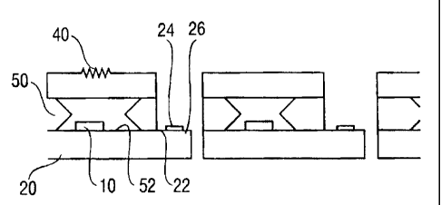
Figure 2A is an exploded side view of the wafer level assembly of a plurality
of
integrated electro-optical modules. As in Figure 1, the submount wafer 20 has
an electro-
optical element 10 thereon with interconnection tracks 22. An optics wafer 30
having
corresponding optical elements 40 formed thereon is also provided. A spacer
wafer 50
separates the optics wafer 30 and the submount wafer 20. The spacer wafer
includes
passages 52 therein which allow light to pass between the optical element 40
and the active
element 10. As shown in Figure 2A, these passages 52 may be formed by etching
when the
spacer wafer 50 is silicon.
In Figure 2A, the spacer wafer 50 also includes indentations 54, here also
formed by
etching, These indentations 54 are provided over the bond site 24 so that upon
separating
along lines 62, 64, the bond site 24 will be accessible in the separated
module, as seen in
Figure 2B. This facilitates electrical connections required to the electro-
optical element 10.
The separating may include dicing the optics wafer 30 and the spacer wafer 50
along line 62
and dicing through all three wafers along line 64. Alternatively, a wide blade
may be used to
dice the entire width between lines 62, 64 through the optics wafer 30 and the
spacer wafer
50, and then using a thin blade to dice only the submount wafer 20. The
attached structure
may be flipped to facilitate dicing of only the submount wafer 20.
CA 02439010 2003-08-22
WO 02/071560 PCT/US02/06688
-6-
An alternative configuration is shown in Figure 3A and 3B, in which the spacer
wafer
includes holes 56 therein over the bond site 24, rather than the indentations
54. The
separating lines 65, 64 remain the same and may be realized in either process
noted above.
However, the resulting structure will not have even edges of the optics wafer
30 and the
spacer wafer 50.
Another configuration is shown in Figures 4A and 4B. Here, rather than forming
the
same active element 10 - bonding site 24 pairs on the submount wafer 20,
adjacent structures
will be mirror images of one another. This allows large indentations 58 to be
placed over two
bonding site 24, 24'. The separating along separating line 76 may be performed
in a
conventional manner. Separating along separating lines 70, 72 is only through
the optics
wafer 30 and the spacer wafer 50, and may be realized either by dicing along
either line or
with a thick dicing blade covering the width of the gap between separating
lines 70, 72. The
submount wafer 20 is then separated along separating line 74, preferably using
a thin blade.
Figure 5 illustrates another configuration, requiring less separating. Here,
the spacer
wafer again includes the holes 56. The optics wafer 30 also includes holes 36,
here etched in
the optics wafer 30, isolating the different optics needed for each module.
Also as shown
herein, the submount 20 includes two electro-optical elements 10, 12 requiring
interconnection. Here the electro-optical elements are different from one
another, with the
electro-optical element 12 being monolithically integrated with the submount
wafer 20.
Additional optical elements 42 are provided on the optical wafer 30 for the
electro-optical
element 12. Here, only separation of the submount wafer 20 along separating
line 80 is
required to realize the individual modules.
Another alternative is shown in Figures 6A-6B. Here, a bonding pad 124 is
provided
on the optics wafer 30. An interconnection line 122 connecting the active
element 10 and the
bonding pad 124 would be on both the mount wafer 20 and the optics wafer 30.
As shown on
CA 02439010 2003-08-22
WO 02/071560 PCT/US02/06688
-7-
Figures 6A and 6B, the bonding between the mount wafer 20 and the optics wafer
30 is via
an electrically conductive material, here shown as solder balls 90.
Alternatively, the spacer
used in the previous configurations could be coated with metal where needed to
provide the
lead from the active element 10 to the bonding pad 24 on the optics wafer 30.
Now the
separating lines 92, 94, 96 lead to a separation of the module that results in
the optics wafer
30 extending beyond the mount wafer 20 in at least one direction, i.e., so
that the bonding pad
124 is easily accessible.
Another alternative is shown in Figures 7A-7B. Here, one bonding pad 124 is
provided on the optics wafer 30 while another bonding pad 24 is provided on
the mount
wafer 20. A spacer wafer 50 is also provided in this configuration. The
interconnection line
122 connecting the bonding pad 124 and the active element 10 would be on the
mount wafer
20, the spacer wafer 50 and the optics wafer 30. As shown on Figures 7A and
7B, the
interconnection line 122 follows the spacer wafer 50 between the mount wafer
20 and the
optics wafer 30. Alternatively, a metal or other electrically conductive
material may be
patterned on the wafer, and the interconnection line 122 being only on the
mount wafer 20
and the spacer wafer 30, with the electrically conductive material on the
spacer wafer 50
providing comiection therebetween. Now separating lines 93, 95, 97, 99 lead to
a separation
of the module that results in the optics wafer 30 extending beyond the mount
wafer 20 in at
least one direction, i.e., so that the bonding pad 124 is easily accessible,
and the mount wafer
20 extending beyond the optics wafer 30 in at least one direction, i.e., so
that the bonding pad
24 is easily accessible.
As shown in Figure 8, a flexible printed circuit board (PCB) 100 may be
directly
attached to the modules formed by any of the above configurations. While the
above
configurations show a cross-section of the modules, it is to be understood
that any of the
electro-optical element - bonding site pairs may be an array thereof, as shown
in module 110
CA 02439010 2003-08-22
WO 02/071560 PCT/US02/06688
-8-
of Figure 8. Due to the separating discussed above, a step 26 formed by the
extension of the
wafer having the bonding sites 24 thereon readily provides electrical
connection to another
device, here a PCB 100. Further, the module 110 may be separated to provide
steps 28 in the
wafer having the bonding pads 24 thereon, here shown as the mount wafer 20, on
either side
of the other wafer, here shown as the optics wafer 30, to facilitate
niechanical strain relief for
the flex lead of the PCB. The steps 28 may extend around the whole perimeter.
Even if electrical interconnections are not to be provided on the steps 28,
when
integrating an optical subassembly formed on a wafer level with a system which
is not t be
stacked as the rest of the wafer assembly, these steps 28 may be used to
provide support
and/or alignment features. For example, as shown in Figure 9, an optical
subassembly 130 to
be mounted in a circuit board 120 having a hole 125 therein for receiving the
optical
subassembly 130 may include steps 128 to provide mechanical support and/or
alignment to
the circuit board. The steps 128 may extend around the entire perimeter of the
optical
subassembly 130. The optical subassembly 130 and the steps 128 may be formed
on a wafer
level. The steps 128 may include alignment features for facilitating alignment
of the circuit
board 120 and the optical subassembly 130. The steps 128 may provide
mechanical
mounting surface for mounting the optical subasseinbly 130 to the circuit
board 120. The use
of the steps 128 for attachment also allows the bonding material to be kept
out of the optical
plane.
It will be obvious that the invention may be varied in a plurality of ways,
such as the
use of different bonding materials, extension in one or more directions, and
different, or no,
spacer configurations. Such variations are not to be regarded as a departure
from the scope of
the invention. All such modifications as would be obvious to one skilled in
the art are
intended to be included within the scope of the appended claims.