Note: Descriptions are shown in the official language in which they were submitted.
08/19/2003 TUE 20:02 FAg ~ 002/043
CA 02439167 2003-08-22
Rub 19 Q3 12:U3P p.21
.r ._~ ~~.~ .
WO 02/067002 PCT/DEOZ/00610
METHOD AND DEVICE FOR TESTING THE QUALITY OF PRINTED
CIRCUITS
The present invention relates to a methbd and a device for
the testing of the quality of printed c~.rcuxts according to the
preamble of Claims 1 arid 10 respectively.
For the quality control during the production and assembly
of printed circuits, a mechanival method has been known which,
using hundreds of contacts, by means of perforated mas7cs as Grell
as by means of contacts made of special alloys, scans a test
specimen mechanically. For the quality test, individual circuits
azs contacted and their function is tested by an electric
measuring adapter.
The electric testing by means of contacts and measuring
adapters produced specifically for this purpose, however,
requ3.res High expenditures and is susceptible to disturbances.
The positioning of the contacts in a measuring adapter is
becoming increasingly difficult as a result of the
miniaturization of the electronic modules. Since a separate
special measuring adapter has to be constructed for each new type
of printed circuit, the costs required for this purpose are
enormous. The construction of a medium-size measuring adapter
1
08/19/2003 TUE 20:02 FAX f~ 003/043
CA 02439167 2003-08-22
fiug 19 03 12:O~p p,22
requirES, ~or example, the production of approximately 50D
special contacts. The required time for such a construction can
be indicated to be approximately 0.5 days. The costs for this
purpose amount to an average of DM 500.00 and, in the case of
SMD--layouts rise rapidly to more than DM 1,000.00_ In the case
of very small series of, for example, 2o printed circuits, it is
often not worthwhile, at a product price of DM 20,00 a piece, to
ir~rrest an additional DM 25_00 of testing cost for each printed
circuit and an additional production day. This particularly
applies to pilot series since, in this case, the next test series
often results in changes to the layout and thus tv the
arrangement of the tESt contacts. Changes of the layout of the
printed circuit therefore lead to expenses for changes on the
electric measuring adapter or for its new construction. However,
if for reasons of cost, a printed ci=cult is not tested, there is
the risk of losing the saved costs many times over in the e~crent
of a faulty production.
A special test algorithm is used during the electric testing
by means of the mQasuring adapter. If, foz example, a narrowing
of a track conductor occurs, this is acknowledged kith the test
result "fault-ft-ee"; that is, such production fau7.'ts are not
recognized. Parasitic lugs are also not detected, which may
result in unusable products, particularly in the case of circuits
for high--frequency applications. Likewise, non-centric drill
holes are also not recognized as faults.
2
08/19/2003 TUE 20:03 FAX ~ 004/043
CA 02439167 2003-08-22
Rug 19 03 12:04p p.23
Another disadvantage of the previous testing method is the
fact that the electric testing does not take place before the end
of the production process, so that the fault can only be detected
very late_ the risk of producing a faulty series rises with the
number of layers. Thus, in the case of an 8-layer multilayer
printed Circuit, the probability of a faulty production is mush
higher than in the case of a Z-layer printed circuit. Up to now,
a multilayer printed circuit had to be completely produced in
order to be able to determine that the first layer was faulty.
Here, the above-described limitations with rQSpect to the
undetectable faults cannot be excluded anyway.
At the printed circuit manufacturers, the storage of
electrical measuring adapters requires high logistical
expenditures_ It is not known which measuring adapters aze
needed when, where or if at all- stored measuring adapters have
to be found again. After an extended storage time, the contact
may be in need of maintenance.
It is an object of the invention to provide a method and a
device of the above-mentioned type which are improved with
respect to the reliability and flexibility of the quality test
while the costs are simultaneously reduced.
According to the invention, this object is achieved by means
of a method of the above-mentioned type with the process steps
3
08/19/2003 TL1E 20:03 FAX ~ 005/043
CA 02439167 2003-08-22
Rub 19 03 lZ:a4p p_24
indicated in Claim L and by Means of a device of the above-
mentioned type with the features characterized in Claim 1o_
Advantageous embodiments of the invention are described in the
additional claims.
According to the invention, the following steps are provided
in the case of a method of the above-mentioned type:
(a) Detecting a radiation originating from a surface of the
printed circuit,
(b) converting the detected radiation to data which
represent a surface structure and/or depth structure of the
printed circuit,
(c) comparing the data of the surface structure and/or of
the depth structure with stored data of a desired condition of
the surface structure and/or depth structure, and
(d) determining deviations between the data of the detested
surface structure and/or depth structure and the data of the
desired condition of the surface structure and/or depth
structure.
This has the advantage that, during an automated mechanical
printed circuit production and assembly, assembling faults as
well as faults in the structure and measurement of the printed
circuits themselves can be detected with a high effectiveness and
quality. As a result of the no-contact functionality,
4
08/19/2003 TOTE 20:04 FAg (~ 006/043
CA 02439167 2003-08-22
Rug 19 G13 lc : 04p p. 25
considerable cost reductions are achieved. Quality controls can
be carried out rapidly and reliably. Costs a,nd time are saved in
comparison to conventional testing methods, in which case, as a
result of an additionally high flexibility, the invention can
also be used economically in a small-scale. p=oductioa. 'fhe
positioning of individual measuring testing devices is
elirninatEd. A miniaturization rcxquired for an adapting to the
structures of the printed circuits to be tested is permitted at
any time_ A mechanical construction for individual test
specimens is eliminated. The testing device becomes operative
within a few seoonds, whereby the testing costs are drastically
reduced. In the event of changes of the layout of the pr~.nted
circuits to be tested, only new data have to be read in in order
to actualize the testing device. As a result, cost-effectively
tested printed circuits are obtained also in the case of small
quantities_ The test result guaranties a virtually 100%
faultlessness and provides a degree of quality which so far had
not been reached.- Smudgily etched track conductors as Well as
smudgy soldering points in the case of equipped printed circuits
are detected as well as non-centric drill holes or incorrectly
milled dimensions of the printed circuit_ Since the testing
method according to the invention can bE used in a rapid, simple
ahd cost-effective manner between all production steps, faulty
series productions can be excluded. As a result, a clear
production advantage is achieved in the case? of the expansive
multilayer printed circuits. Because of the easy manageability
08/19/2003 TLTE 20:04 FA% X1007/043
CA 02439167 2003-08-22
Rug 19 O3 12:05p p_26
of data, large quantities of different test specimens can be
stored while the space requirement is lo~sa. Furthermore, the
quality-related demands, fos example, of aeronautical and space-
flight engineering can be met. In addition, proof of quality
regarding aZZ production processes can be supplied for each
individual product.
The detected data as well as the data of the desired
condition are preferably data in digital form_
Expediently, according to Step (d), the deviations are
compared faith corresponding tolerance bands and, as a gunetion of
this comparison, a ~~faultless" test result is generated when the
deviations are within the tolerances bands, or a "faulty" test
result is genez~ated when the deviations are at Least partially
outside the tolerance bands.
In a preferred embodiment, in Step (a), the surface
structure and/or depth structure is detected by means of
electromagnetic waves r8flected by the surface and/or transmitted
by the latter, particularly light visible in the.frequency
spectrum, x-rays, radar nays, microwave rays and/or infrared
radiation.
From corresponding changes of the temperature over the time,
conclusions can therefore be drawn concerning the structural
6
08/19/2005 TtTE 20: 04 FAX I~ 008i 04a
CA 02439167 2003-08-22
Rug 19 03 12:05p p.27
situations on the su=faca and in the depth that in Step (a),
thermal radiation radiated by the su=face is detected and in Step
(b), from a change of the thermal radiation over the time, the
surface structure and/or depth structure is ans,lyaed.
For ca=tying out a dynamic measurement, the pritrted circuit
is heated or Gaoled during the measurement in Step (a).
For example, the detection in Step (a) is carried out by
means of a thermo-optical difference measurement.
For a corresponding documentation concerning each printed
circuit, the deviations of Step (b) axe stored in a mass memory.
A test which can be implemented rapidly is achieved in that
the data of the desired condition of the surface structure are a
layout of the printed circuit designed during the planning.
According to the invention, a device of the above-mentioned
type is characterized by a sensor for detecting a radiation
originating from a surface of the printed circuit; a device for
converting the detectQd radiation to data which represent a,
surface structure and/or depth structure of the printed circuit;
a dEVice for comparing the data of the surface structure and/or
the depth structure with stored data of a desired condition of
the surface structure and/or depth structure; and a device for
7
08/19/2003 TUE 20:05 FAX X1009/043
CA 02439167 2003-08-22
Flug 19 03 12:O5p p.2a
determining deviations between the data of the detected surface
structure and/or depth structure and the data of the desired
condition of the surface structure and/or depth structure.
This has the advantage that, during an automated mechanical
printed circuit production and assembly, assembling faults as
well as faults in the structure and measurement of the printed
circuits themselves can be detected with a high effectiveness and
quality. As a result of the no-contact functionality,
considerablQ cost reductions are achieved. Quality controls can
be carried out rapidly and reliably_ Costs and time are saved in
comparison to conventional testing methods, in which case, as a
result of an additionally high flexibility, the invention; care
also be used economically in a small-scale production. The
positioning s~f individual measuring testing devices is
eliminated. A miniatuz-ization required for an adapting to the
structures of the printed circuits to be tested is permitted at
any time. A mechanical construction for individual test
specimens is~eliminated. The testing device becomes pperative
within a few seconds, whereby the testing costs are drastically
zeduced. In the event of changes of the layout of the printed
circuits to be tested, only new data ha~cr~e to be read in in order
to actualize the testing device. As a result, cyst-effectively
tested printed circuits are obtained also in the case of small
quantities. The test result guaranties a virtually 7.0o%
faultlessness and pro«ides a degrEe of quality which so far had
8
08/19/2003 TUE 20:o5 FAg ~ 010/043
CA 02439167 2003-08-22
Rub 19 03 12:05p p_29
not been reached. Smudgily etched track conductors as well as
smudgy soldering points in the case of equipped printed circuits
are detected as well as non-centric drill holes or incorrectly
milled dimensions of the printed circuit. 6ince the testing
method according to the invention can be used in a rapid, simple
and cost-egfective manner between all production steps, faulty
series productions can be excluded_ As a result, a clear
production advantage is achieved in the case of the expensive
multilayer printed circuits. Because of the easy manageability
of data, large quantities of different test specimens can be
stored while the space requirement is low. Furthermore, the
quality-related demands, foz example, of aeronautical and space-
flight engineering can be met. In addition, proof of quality
regarding all production processes can be supplied for each
individual product.
The detected data as well as the data of the desired
condition are preferably data in digital form.
Expediently, a device is provided for comparing the
deviations with corresponding tolerance bands, which device, as a
function of this comparison, generates a test result "fault-free"
for the printed circuit if the deviations are within the
tolerance bands, or it generates a test result of "faulty" if the
deviations are at least partially outside the tolerance bands_
9
08/19/2003 TLTE 20;08 FAX X1011/043
CA 02439167 2003-08-22
Rug 19 03 i~:DSp p.30
In a preferred embodiment, the sensor is constructed for
detecting electromagnetic waves, particularly in the frequency
spectrum of visible light, x-rays, radar rays, microwave rays or
infrared radiation and is arranged such that it detects
electromagnetic waves reflected by the printed circuit and/or
transmitted by it.
For example, the senso~c is constructed for detecting heat
radiation from the surface of the printed cixcuit, and the device
for converting the detected radiation to data, which represent
the surface structure and/or depth structure of the printed
circuit, is constructed such that this device analyzes the
surface structure and/or depth structure from a change of the
heat radiation over the t~.me at a certain point of the printed
circuit and/or over the surface of the printed circuit.
For implementing a dynamic measurement, a device,
particularly a laser, is provided for cooling oz heating the
printed circuit during the xnc~asurement.
The device is, for example, constructed for carrying out a
thermo-optical difference measurement.
For the documentation of the test results for each
individual printed circuit, the device, in addition, has a mass
memory for storing the deviations.
l0
08/19/2003 TLTE 20: 08 FAg f~ 012/043
CA 02439167 2003-08-22
Rub 19 03 1~:06p p.31
In a particularly preferred embodiment, the sensor is at
least one pyro sensor or a thermal image camera. As an
alternative, the sensor ooinprises a laser.
A testing position which can be built up in a rapid, simple
and cost-effective manner can be achieved in that the device f0=
converting, the device for comparing arid the device for
determining deviations are constructed in a computer_ As a
result, only the software and a database have tp be adapted to
the pri'rited circuit tv be tested in a concz-ete man77er_ A
hardware adaptation of the testing device to the layout of the
printed circuit aze completely eliminated.
The invention will be explained in detail in the following
by means of the drawing. In the single figure, this drawing
shows a schematic block diagram of an embodiment of a devicE
according to the invention for implementing the method according
to the invention.
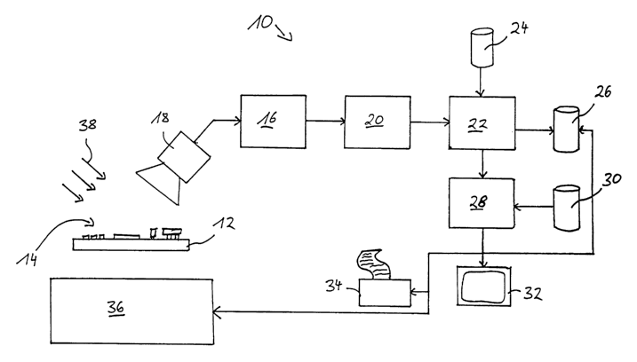
The embodiment of the device 10 according to the invention
illustrated in the figure for testing printed circuits 12 having
a su7rface structure 14 comprises a device 16 for detecting the
surface structure 14 of the printed circuit 1Z by m8ans of a
sensor 18, a device ZO for converting the detected surface
structure 14 to digital data, a device 2Z far cvmpa7ring the
digital data of the surface structure 14 with digital data of a
11
08/19/2003 TUE 20:07 FAB X1013/043
CA 02439167 2003-08-22
Rug 19 03 12:06p p.32
desired condition of the surface structure stored in a memory 24
and for determining deviations between the digital data of the
detected surface structure 14 and the digital data of the desired
condition of the surface Structure from the memory 2a_ These
deviations are stored in a mass memory 26 and are supplied to a
device ~8 for comparing the deviations with corresponding
tolerance bands which are filed in a memory 30. As a function of
this comparison, the dEVice 28 generates the test result "fault-
free" for the printed circuit 14 when the deviations are within
the tolerance bands, or "faulty" whsn the deviations are at least
partially outside the tolerance bands.
This test result is stored in the mass memory 26, is shown
oz~ a display device 32, is fed to a printer 34 Which prints out a
protocol on-line, as well as to a process control 36. The
process control 36 sorts the printed circuit 12, if required,
automatically out of the production line wrhen it receives the
test result "faulty" from the device 28.
The sensor 18 is, for example, a,n optical sensor which
receives electromagnetic waves 38 from the Visible spectrum,
infrared range, x-rays, radar rays after the ref lection on the
surface structt~.re 14 of the p=inted circuit 12 and feeds them to
an image processing or image recognition device constructed in
the device 16.
1Z
08/19/2003 TUE 20:07 FAg C~]o14/043
CA 02439167 2003-08-22
Rug 19 O3 12:06p p.33
Because of the simple and low-cost cohst~uction of the
testing device 10, the latter, as required, is provided at
several points in the production sequence for the printed eiZCUit
12. For example, during the production of printed circuits 12
with several layers, the surface structure 14 can be tested after
each layer production.
The comparatiVC data in the memory 24 ate the data of the
layout from the design of the punted circuit 12. Currently,
this design is exclusively produced in a computer-aided manner,
so that these layout data are present directly as digital data
and, if required, have to be correspondingly converted only for
the comparison in the device 2~. In other words, a material
structure 14 of the printed circuit 12 is therafo=e quEried in a
no-contact manner by means of the sensor 18 as the actual value
and is compared with the desired value, specifically the layout
data of the CAp design of the printed circuit. The tolerance
bands in the memory 3o will then define permissible deviations of
the actual values according to the detected depth structure from
the desired values according to the data memory 24. If values
leave the tolerance bands, the printed circuit 12 is classified
as faulty by the device Zs and can then immediately be pulled out
of the running process. ~s required, the process control 36
provides a correction of process parameters in order to
counteract a systematic fault on the printed circuits 12. If an
intervention of operating personnel in the production sequence is
13
08/19/2003 TLJE 20: 08 FAg ~] 015i 043
CA 02439167 2003-08-22
Rug 19 03 12:06p p.34
necessary, the process control 35 stops the production and
supplies a corresponding message_ As a result, an undESirable
and possibly cost-intensive production of rejects is effectively
avoided.
It Was found to be particularly advantageous that the method
according to the invention and the device according to the
invention respectively carry out the test in a no-contact manner.
Since no mechanical contacts are required between the testing
device 1o and the test specimen, specifically the printed circuit
Z2, on the part of the testing device 10, no hardware adaptation
to the layout of the printed circuit 12 has to be carried out_
The only adaptation takes place on a~software level, particularly
in the case of the data in memories Z4 and 30. The testing
device 1o can be adapted to changes 0g the layout by simple
clicking_
The printout from the printer 3~ and the data in the memory
26 are used for documentatioh, ih which case, it can easily be
achieved that all test results can also still later be assigned
to a certain printed circuit from different points in the
production sequence. As a result, a complete testing protocol
with the proof of a correct production can be added to the
finished printed circuit. The data in the mass memory Z6 have an
unlimited storage time without special storage costs and, as
required, can be made available worldwide via the Internet_
~4
08/19/2003 TUE 20:08 FAI 1ø]018/043
CA 02439167 2003-08-22
Rub 19 03 12:O6p p.35
An interface between the sensor and the computer has to be
established only once and is independent of the type and layout
of the printed cizcuit.
A thermo-optical difference measurement is particularly
preferable. For this purpose, a thermal radiation originating
from the surface of the printed circuit 12 is detected by the
sensor 18 and analyzed in the device xs. In this case,
conclusions can be drawn on the surface structure as well as on
the depth structure of the printed circuit 12. For example, an
analysis of the change of the thermal radiation over the surface
of the printed circuit takes place, that is, of the different
thermal radiation at different points on the printed circuit,
which immediately indicates a surface structure. As an
alternative or in addition, the printed circuit is heated and the
change of the thermal radiation is detErmined at cErtain points;
that is, in other words, a heating gradient is determined. For
example, in this manner, feedthroughs in the printed circuit can
be checked; that is, in the widest sense, the dQpth structure
within the printed circuit can be checked. Because of the larger
mass absorbing heat, a completely constnacted feedthrough Will
heat up more slowly than an incomplete feedthrough, so that the
latter can be identiFied in a no-contact, simple and rapid
manner. Instead of the measurement of the change of the thermal
radiation over the time during the heating, also after the
08/19/2003 TOTE 20:09 FAg f~ol7/043
CA 02439167 2003-08-22
Rub 19 03 12:07p p.36
heating of the printed circuit, the change of the thermal
radiation over the time during the cooling may be recorded_
Here, for example, a complete feedthrough, because of the larger
mass containing a larger amount of heat, will cool more slowly
than an incomplete feedthrough, so that the latter fault on the
printed circuit 12 can be determined in a simple, rapid, no-
contact, non-destructive manner also after the completion of the
printed circuit 1z_
1C