Note: Descriptions are shown in the official language in which they were submitted.
CA 02439378 2003-08-26
WO 02/069551 PCT/US02/03217
[0001] INITIAL CELL SEARCH ALGORITHM
[0002] BACKGROUND
[0003] The present invention generally relates to user equipment (UE)
synchronization to a base station. More particularly the present invention
relates to a
cell search system which utilizes an improved initial cell search algorithm.
[0004] Initial cell search algorithms are used to synchronize the UE to a base
station. The UE accomplishes this procedure via a common downlink channel
called
the physical synchronization channel (PSCH). Referring to Figure 2, the PSCH
has
a structure wherein the same primary synchronization code (PSC) is transmitted
at the
beginning of each slot, while a secondary synchronization code (SSC) is
transmitted
for each slot, resulting in fifteen (15) different SSCs. As those skilled in
the art know,
a frame that is fifteen (15) slots long can transmit fifteen (15) SSCs.
[0005] The transmit order of the SSC depends on the primary scrambling code
group number. As an example, in a five hundred and twelve (512) cell system,
there
are sixty four (64) groups. In each group, the patterns of the SSC and its
cyclic shifts
are different. As a result, there are five hundred and twelve (512) primary
scrambling
codes. Each cell, of a five hundred and twelve cell (512) system, is assigned
a code
such that no one code is used by more than one cell in a given reception area.
[0006] Therefore the cell search synchronization systems determine the primary
scrambling code of a cell utilizing an initial cell search algorithm. Common
initial cell
search algorithms utilize three (3) major algorithms: a step 1 algorithm
detects the
PSC and determines a chip offset; a step 2 algorithm uses the information
given by step
1 and detects the slot offset and code group number; and a step 3 algorithm
utilizes the
information provided by the step 2 algorithm and detects the primary
scrambling code.
Unfortunately, each step algorithm has an inherent error associated with it.
The error
present in each of the steps is caused by the UE detection of noise associated
with the
-1-
CA 02439378 2007-01-19
received common downlink channel, which can result in a high number of false
detections.
[0007] Also, the common initial cell search algorithms can not handle a
rejection by the upper layers of the wrong public land mobile network (PLMN).
Since
most algorithms detect the strongest cell in the common downlink channel, it
is likely
that each time the algorithm locates a cell the same PLMN will be associated
with the
cell. This results in a deadlock and ultimately an indication to the UE that
there is no
service.
[0008] Accordingly, there exists a need for a system and method that reduces
the number of false detections by the initial cell search algorithm and is
able to
overcome the deadlock associated with a rejection due to the wrong PLMN.
[0009] SUMMARY
[0010] The present invention is a system and method for establishing a
communication link between a user equipment (UE) and a base station in a
communication network, comprising the steps of sampling an incoming
communication signal, wherein said sampling includes generating even and odd
signal
samples of said communication signal, approximating a signal strength
magnitude for
each of the signal samples, accumulating the signal strength magnitudes of the
signal
samples, identifying a peak sample, wherein said peak sample is the signal
sample
with a highest accumulated signal strength magnitude, assigning an index value
to the
peak sample, wherein said index value indicates a chip location of a primary
scrambling code, assigning a chip offset to the index value based on said
index value,
determining a code group number and slot offset based on the chip offset,
retrieving
the primary scrambling code based on the code group number and slot offset,
and
adjusting a search frequency of a UE based on said primary scrambling code.
-2-
CA 02439378 2007-01-19
[0011] BRIEF DESCRIPTION OF THE DRAWINGS
[0012] Figure 1 is an illustration of the initial cell search system made in
accordance with the preferred embodiment of the present invention.
[0013] Figure 2 is an illustration of the physical synchronization channel
(PSCH).
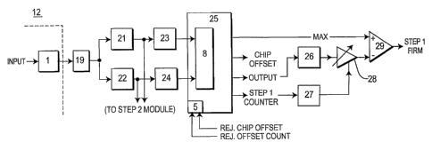
[0014] Figure 3 is a block diagram of the step I module in accordance with the
preferred embodiment of the present invention.
[0015] Figure 4 is a flow diagram of the step 1 module in accordance with the
preferred embodiment of the present invention.
[0016] Figure 5 is a block diagram of the step 2 module in accordance with the
preferred embodiment of the present invention.
[0017] Figure 6 is a graphical illustration of the Fast Hadainard Transform
(FHT) structure.
[0018] Figure 7 is an illustration ofthe input matrix structure in accordance
with
the preferred embodiment of the present invention.
[0019] Figure 8 is an illustration of the code group matrix structure in
accordance with the preferred embodiment of the present invention.
[0020] Figure 9 is an illustration of the correlation matrix structure in
accordance with the preferred embodiment of the present invention.
[0021] Figures l0A and lOB show a flow diagram of the step 2 algorithm in
accordance with the preferred embodiment of the present invention.
[0022] Figure 11 is a block diagram of the step 3 module in accordance with
the
preferred embodiment of the present invention.
[0023] Figure 12 is a block diagram of the step 3 correlator in accordance
with
the preferred embodiment of the present invention.
-3-
CA 02439378 2003-08-26
WO 02/069551 PCT/US02/03217
[0024] Figures 13A and 13B are a flow diagram of the step 3 algorithm in
accordance with the preferred embodiment of the present invention.
[0025] Figures 14A and 14B show a flow diagram of the controller cell search
decision logic in accordance with the preferred embodiment of the present
invention.
[0026] Figures 15A and 15B show a flow diagram of the controller window
exclusion logic in accordance with the preferred embodiment of the present
invention.
[0027] DETAILED DESCRIPTION OF THE PREFERRED EMBODIMENT
[0028] The cell search synchronization system 10 in accordance with the
preferred embodiment of the present invention is illustrated in Figure 1. The
system
comprises a step 1 module 12, a step 2 module 14, a step 3 module 16, and a
controller 18 to accomplish synchronization between a user equipment (UE) and
a base
station. In order to accomplish this synchronization, the UE, through the cell
search
synchronization system 10, utilizes an initial cell search algorithm, to be
disclosed
hereinafter.
[0029] The step 1 algorithm of the initial cell search algorithm is
accomplished
using the step 1 module 12. Referring to Figure 3, the step 1 module 12
coinprises two
Hierarchical Golay Correlators (HGC) 21, 22, two absolute value modifiers
(AVM)
23, 24, a decision circuit 25, a normalizer circuit 26, a look up table 27, a
multiplier
28, a splitter 19, and a step 1 comparator 29. The root raised cosine filter
(RRCFIR)
1 shown is not a part of the step 1 module 12, but are illustrated therein to
provide a
complete picture.
[0030] The purpose of the step 1 module 12 is to find the strongest path over
a
frame worth of samples the UE has detected and determine the chip offset of
the
strongest path. The RRCFIR 1 coupled to the splitter 19 is a pulse shaped
filter that
samples the downlink communication signal from the base station at twice the
chip rate
and forwards the sample signal to the splitter 19. The splitter 19 splits the
sainpled
signal into its even and odd samples and passes them to HGCs 21, 22.
-4-
CA 02439378 2003-08-26
WO 02/069551 PCT/US02/03217
[0031] The HGCs 21, 22 are coupled to the AVMs 23, 24, and the sample
selector 34 of the step 2 module 14 (illustrated in Figure 5), to be disclosed
hereinafter.
HGCs 21, 22 correlate the PSC of the input signal. As those skilled in the art
know,
the HGCs 21, 22 output the complex values of the even and odd samples of the
input
signal, respectively. The HGC 21, 22 outputs are forwarded to the AVMs 23, 24
and
the sample selector 34.
[0032] The AVMs 23, 24, coupled to the HGCs 21, 22 and the decision circuit
25, determine the magnitudes ofthe HGCs 21, 22, equation to generate the
magnitudes
is determined according to the following equation :
abs(x)- max(Ixrealj, Iximagj) + 0=5*minQxreall, Xm,J) Equation 1
The use ofthe approximated absolute value in accordance with Equation 1
reduces the
hardware required in this implementation and causes no significant performance
degradation. Once the approximated absolute values have been determined by the
AVMs 23, 24, respectively, the modified even and odd samples are output to a
decision circuit 25.
[0033] The decision circuit 25, coupled to the AVMs 23, 24 and the controller
18, determine the chip offset. The modified even and odd samples output from
the
AVMs 23, 24 are input into a 1VIUX 8 within the decision circuit 25, and
combined
into a single stream. This stream is a representation of the strength of the
signal
transmitted in one of the samples of each slot of each frame. As illustrated
in Figure
2, there are two thousand five hundred and sixty (2560) chips in each slot and
fifteen
(15) slots in each frame. Since the input signal is sampled at twice the chip
rate, there
are 5120 samples in each slot. Therefore, the decision circuit 25 determines
the
location of the PSC in the signal, chip offset, by sweeping through the 5120
accumulated samples at the end of each slot.
-5-
CA 02439378 2003-08-26
WO 02/069551 PCT/US02/03217
[0034] The stream generated by the 1V1TJX is forwarded to an accumulator (not
shown) within the decision circuit 25. This accumulator has a five thousand
one
hundred and twenty (5120) sample long register which stores the accumulated
sample
value for each slot of every frame, and operates on the slot rate. The
strength of the
signal for each sample in a slot is added to the strength of the signal of
each sample in
every subsequent slot. As an example, the samples of slot 1 comprise the
following
signal strength values { 1,5,3,7}; the samples of slot 2 comprise the
following signal
strength values {2,4,8,3}. Initially, the registers of the accumulator have
the values
{0,0,0,0}. As each sample value from slot 1 is added to the registers of the
accumulator, the register values change accordingly. For instance, when the
first
sample value of slot 1 is added to the first register value, the accumulator
has the
values { 1,0,0,0}; when the second sample value of slot 1 is added to the
second
register value, the accumulator has the values { 1,5,0,0} and so on. Once the
last
sample value of slot 1 is added to the accumulator, the first sample value of
slot 2 is
added to the first register of the accumulator, resulting in the accumulator
having the
values {3,5,3,7}; when the second sample value of slot 2 is added to the
second
register value, the accumulator has the values {3,9,3,7}. The preferred
embodiment
of the present invention, flushes the registers of the accumulator after five
(5) frames
have been accumulated, which is equivalent to seventy five (75) slots. The
number of
accumulated frames is counted by a step l counter (not shown) within the
decision
circuit 25.
[0035] A decision, determination of the chip offset, by the decision circuit
25
is generated at the end of each frame, fifteen (15) slots. The decision
circuit 25
determines which register in the accumulator has the maximum accumulated
sample
value MAX and assigns an index to it. The index corresponds to the half chip
location
of the PSC signal for the base station with the strongest signal.
[0036] Chip offset assignment is determined using the HGC offset value of 511.
As those skilled in the art know, the output of the HGC are delayed by 256
chips.
-6-
CA 02439378 2003-08-26
WO 02/069551 PCT/US02/03217
Therefore, when the decision circuit 25 assigns an index in the peak sample,
the HGC
offset value must be subtracted. Since the PSC is 256 chips long, 512 samples
long,
subtracting the HGC offset from the index equates to setting the chip offset
to the
beginning of the slot. If the index generated by the decision circuit 25 is
greater than
the HGC offset value of 511 then the chip offset is calculated in accordance
with
Equation 2 below:
chip_offset = INDEX - 511 Equation 2
If the index is less than the HGC offset value then the chip offset is
calculated in
accordance with Equation 3 below:
chip_offset = 5120 + INDEX - 511 Equation 3
[0037] As illustrated in Figure 3, the decision circuit 25 also comprises a
mask
generator 5, which is used to exclude a window around a rejected chip offset
from
detection by the decision circuit 25. This mask generator 5, therefore,
prohibits the
decision circuit 25 from utilizing an index associated with a rejected chip
offset. The
details of the mask generator 5 will be disclosed hereinafter.
[0038] The calculated chip offset and the frame count step 1 counter are
output
to a controller 18, to be disclosed hereinafter. The decision circuit 25 also
outputs the
maximum accumulated chip value MAX and the accumulated chip value OUTPUT for
all registers.
[0039] The accumulated chip value OUTPUT for all registers is output to a
normalizer circuit 26, where it is sampled at 20% the chip rate (one out of
five),
summed, and then normalized to 1024. The frame count step 1 counter is output
to the
lookup table 27 to deterinine the proper gain factor based on the number of
fraines
accumulated. The output of the normalizer circuit 26 and the lookup table 27
are then
-7-
CA 02439378 2003-08-26
WO 02/069551 PCT/US02/03217
multiplied by the multiplier 28. The output of the multiplier 28 is considered
the Noise
Threshold and is forwarded to a step 1 comparator circuit 29, to be compared
to the
maximum accuinulated sample value MAX. If the maximum accuinulated sample
value MAX is greater than the Noise Threshold, the differential amplifier 29
outputs
a high stepl firln signal to the controller, indicating a good decision for
step 1,
otherwise a low signal is output.
[0040] As stated earlier, the chip offset and other outputs are determined at
the
end of every frame. Therefore, the reliability of the first decision is less
than that of
the second because the second decision is made over thirty slots instead of
fifteen
slots. The reliability increases as the number of slots accumulated increases.
The
highest reliable output is generated at the Mlth frame, Ml being an integer
greater
than or equal to one (1). The controller 18 resets the frame count step 1
counter and
the accumulator registers at the end of every Mlth frame. The performance
results
under different channel impairment show that five-frame integration is good
enough
to detect PSC. However, this integration can be changed to more or less
frames.
[0041] A flow diagram of the step 1 module is illustrated in Figure 4. The UE
detects the receipt of communications over the common downlink channel (step
401)
and samples the signal at twice the chip rate generating even and odd samples
(step
402). These even and odd samples are passed to the hierarchical Golay
correlators
(HGC) 21, 22 (step 403). The HGCs 21, 22 then forwards the outputs to the AVMs
23, 24 and sample selector 34 (step 404). The AVMs 23, 24 approximate the
magnitudes of the even and odd outputs received from the HGCs 21, 22 (step
405) and
forwards them to the decision circuit 25 (step 406). Upon receipt of the
output
magnitudes the decision circuit 25 combines the magnitudes (step 407), which
represents the signal strength of the signal transmitted in one of the samples
of each
slot of each frame. The signal strength for each sainple is accumulated for
all slots
within each fraine (step 408). The decision circuit 25 then determines which
sample
in the frame has the maximum accumulated sample value (step 409) and assigns
an
-8-
CA 02439378 2004-03-17
index to it (step 410). Based on the index, a chip value is assigned to the
index (step
411), known as the chip offset, and output to the controller 18 (step 412). A
noise
threshold value is then generated using the accumulated chip value for all
samples and
the frame count (step 413) and then compared to the maximum accumulated sample
value (step 414), indicating a firm or tentative decision to the controller 18
(step 415).
[0042] Referring back to Figure 1, the outputs of the step 1 module 12, the
chip
offset, step 1 firm, and step 1 counter, are forwarded to the controller 18.
The controller
18 forwards the chip offset to the step 2 module 14. As stated above, the step
2 module
14 utilizes a step 2 algorithm which takes the chip offset output from step 1
and the HGC
21, 22 outputs and detects the slot offset and the code group number. The step
2 module
14 illustrated in Figure 5, comprises a step 2 comparator 30, a delay 32, a
sample
selector 34, a conjugator 36, a complex multiplier 38, a Fast Hadamard
Transform (FHT)
33, an envelope remover 31, an input matrix generator 35, an RS encoder 37,
and a step
2 decision circuit 39.
[0043] The purpose of the step 2 algorithm is to provide the step 3 algorithm
with
the scrambling code group number and the slot offset. The chip offset from the
step 1
module 12 is sent from the controller 18 to a delay 32 of the step 2 module
14. The chip
offset is delayed for a frame through the delay 32 in order to allow the step
1 module to
make a first decision. The delayed chip offset is then forwarded to the sample
selector 34
which is coupled to the delay 32, a conjugator 36 and the HGCs 21, 22 of the
step 1
module 12. Using the index determined by the decision circuit 25, the sample
selector 34
extracts the peak HGC 21, 22 outputs from the input signal, which are then
conjugated
by the conjugator 36 and output to the complex multiplier 38.
[0044] The same communication signal to the step 1 module 12 is input to an
alignment circuit 15, which aligns the input signal so that step 2 module 14
begins its
search for the scrambling code group number and slot offset at the beginning
of the slot.
Once the signal is aligned, the alignment circuit 15 forwards it to the step 2
module 14.
Even though there are two thousand five hundred and sixty (2,560) chips
-9-
CA 02439378 2003-08-26
WO 02/069551 PCT/US02/03217
in each slot, it should be apparent from Figure 2 that the PSC is located
within the first
256 chips of each slot. Since the chip offset has been determined by the step
1
module, the step 2 module determines the SSC using the location of the
strongest PSC
in the first 256 chips in each slot. As those skilled in the art know, when
SSC codes
are generated, an envelope sequence is applied to the rows of an Hadamard
matrix in
order to have some orthogonality between PSC and SSC codes. This envelope has
to
be removed before proceeding into the remaining portion of the step 2
algorithm. This
envelope removal is accomplished by the envelope remover 31.
[0045] Once the envelope has been removed from the input signal, the signal is
output from the envelope remover 31 to the FHT transform 33 coupled to the
envelope
remove 31 and multiplier 38, which reduces the complexity of the pure Hadamard
correlation operation. Figure 6 is an illustration of the FHT structure. The
output of
the FHT transform 33 is multiplied by the conjugate of the peak HGC 21, 22 by
the
complex multiplier 38 coupled to the conjugator 36 and the FHT transform 33.
The
use of the conjugate of the peak output from the HGCs 21, 22 provides a phase
correction to the FHT output and transforms the one entry that corresponds to
the
transmitted SSC code onto the real axis.
[0046] Once the FHT transform 33 output has been multiplied in the complex
multiplier 38, the real part of the FHT outputs are forwarded to the input
matrix
generator 3 5 by the multiplier 3 8, which puts the FHT outputs into a real
matrix of 15
X 16, called the input matrix. In the input matrix, there are fifteen (15)
slots and in
each slot sixteen (16) elements for a frame. The input matrix is updated per
frame.
The input matrix is then forwarded to the decision circuit 39 where a
determination of
the slot offset and code group number are made. The structure of the input
matrix is
illustrated in Figure 7.
[0047] A correlation matrix is generated within the step 2 decision circuit 39
using the input matrix 35 and a known code group inatrix, which results in a
64 X 15
matrix. The correlation matrix is reset when the frame counter for the step 2
module
-10-
CA 02439378 2003-08-26
WO 02/069551 PCT/US02/03217
reaches M2, similar to that disclosed in the step 1 module. In order to
generate the
correlation matrix, the decision circuit 39 steps through each of the elements
of the
code group matrix and the elements of the input matrix 35 in accordance with
the
equation 4 below:
corrMatrix[i] [j]+= Equation 4
inputMatrix [k] [code_group_matrix [i] [k]]
where j is an integer incremented from 0 to 14 by 1, that represents cyclic
shifts
performed on the identity matrix with respect to columns; i is an integer
incremented
from 0 to 63 by 1; and k is an integer incremented from 0 to 14 by 1. The
structure of
the code group matrix and the resulting correlation matrix are illustrated in
Figures 8
and 9 respectively. Once the correlation matrix has been generated, the
maximum
entry is found by the decision circuit 39. The corresponding row of the found
maximum entry is the code group number and the column is the slot offset.
[0048] Similar to the step 1 module 12, if the max correlation MAX 2 is
greater
than the threshold, the coinparator circuit 30 will output a high step 2 finn
signal to the
controller 18 indicating a firm decision, otherwise a low signal is output
indicating a
tentative decision. The threshold value is calculated using the mean magnitude
value
of the correlation matrix:
63 14 Equation 5
Th = k 960 mag(c~ )
i=o j=0
k=5.12, Pfa =10-4
where PFA is the probability of false alann. The step 2 module 14 outputs to
the
controller 18 the code group number, slot offset, step 2 firm, and step 2
counter.
-11-
CA 02439378 2003-08-26
WO 02/069551 PCT/US02/03217
[0049] The flow diagrain for the step 2 algorithm is illustrated in Figure 10.
The
step 2 module receives the cominunication signal from the base station over
the
downlink channel (step 1001). An envelope sequence is removed from the
communication signal (step 1002a) and output to an FHT transfonn 33, (step
1003a).
At the same time, the chip offset from the step I module 12 is input to a
delay 32 in
the step 2 module 14 (step 1002b) and forwarded to a sainple selector 34,
which
extracts the peak even or odd output generated by the HGCs 21, 22 of the step
1
module 12 based on the chip offset (step 1003b). The output of the FHT
transformer
33 is then multiplied by the conjugate of the peak even or odd sample output
from the
sample selector 34 (step 1004) and transforms one entry of the FHT output that
corresponds to the SSC code onto the real axis (step 1005). The real part of
the FHT
outputs for each slot in a frame are forwarded to the input matrix generator
35 (step
1006). The input matrix generator 35 then creates the input matrix (step
1007). The
input matrix is then forwarded to the decision circuit 39 to determine the
slot offset
and code group number (step 1008). Utilizing the input matrix and known code
group
matrix, the decision circuit 39 generates a correlation matrix (step 1009).
Once the
correlation matrix has been generated, the decision circuit 39 locates the
maximum
entry in the correlation matrix (step 1010), for which the corresponding row
of the
found maximum entry is determined to be the code group number and the column
is
the slot offset. The code group number and the slot offset are then forwarded
to the
controller 18 (step 1011). A threshold value is then calculated using the mean
magnitude value of the correlation matrix (step 1012) and compared to the max
correlation (step 1013), forwarding an indication of a firm or tentative
decision to the
controller 18 (step 1014).
[0050] The chip offset output from the step 1 module 12 and the slot offset
and
code group number output from the step 2 module, are forwarded by the
controller 18
to the step 3 module 16, which utilizes a step 3 algorithm for the purpose of
determining which one of the primary scrambling codes is coming with the least
-12-
CA 02439378 2004-03-17
probability of false alarm (PFA) when the code group number is given. There
are eight
primary scrambling codes in each code group.
[0051] The block diagram of the step 3 module 16 is illustrated in Figure 11.
Similar to the step 2 module 14, the communication signal is input to a second
alignment
circuit 17 which aligns the input signal so that the step 3 module 16 begins
its search for
the scrambling code number at the beginning of the frame. Once the input
signal has
been aligned, the alignment circuit 17 forwards the input signal to the step 3
module 16.
The step 3 module comprises eight (8) scrambling code generators 40, ...408,
eight (8)
correlator circuits 41, ...41 g, a noise estimator circuit 42, a step 3
decision circuit 44, a
decision support circuit 45, a gain circuit 46, and a comparator circuit 47.
The code group
number generated by the step 2 module 14 is input to the eight (8) scrambling
code
generators 40, ...408 and scrambling codes are generated therefrom. The output
of the
scrambling code generators 401...408 is forwarded to the scrambling code
correlators
411...41 g, respectively.
[0052] Along with the scrambling codes output from the scrambling code
generators 40j...408, the communication signal, after processing by an
alignment circuit
17 using the chip offset and slot offset output from the controller 18, is
input to the
correlators 411...418, The correlators 411...418 utilize non-coherent
integration over a
certain number of slots. Integration can be over multiple frames. The
correlation is made
coherently for each symbol that corresponds to the 256-chip data. The absolute
value of
the correlation results are accumulated over 10 * N symbols per frame, where N
is the
number of slots to be accumulated from the beginning of a frame. In a single
slot there
are ten 256-chip long data parts; therefore, ten 256-chip coherent correlation
and ten
accumulations are made per slot. Figure 12 shows the details of a correlator
411.
[0053] After the correlators 411...41g generate the outputs, the maximum
output
and its index have to be found. The step 3 decision circuit 44 takes the
outputs of the
scrambled code correlators 411...418, determines the correlator 411...418 with
the
-13-
CA 02439378 2003-08-26
WO 02/069551 PCT/US02/03217
maximum output, and generates an index thereof. The index is the scrambling
code
number. The scrambling code number is then forwarded to the decision support
circuit
45 and the controller 18. The decision support circuit 45 observes the last M3
decisions made by the decision circuit 44. If a code repeats itself more than
k
repetitions out of M3 inputs, then the code that has been repeated is the
scralnbling
code number that is output from the decision support circuit 45 to the
controller 18.
However, the output of the decision support circuit 45 is only utilized when
there is
no firln decision over the consecutive M3 frames. Even though the decision
support
circuit is only illustrated in the step 3 module 16, a decision support
circuit 45 as
disclosed in the step 3 module 16 can be utilized for both the step 1 and step
2
modules 12, 14 disclosed herein above.
[0054] A firm decision is indicated when the determined maximum correlation
value is greater than the calculated threshold value. The threshold value is
calculated
using the noise estimator circuit 42, which is used for noise measurement, and
a gain
factor. The noise is determined by taking the magnitude of the difference
between the
successive common pilot symbols. This method of noise estimation eliminates
any
bias in the noise estimate due to orthogonal signal interference. The result
of the noise
estimator 42 is multiplied by the gain factor in the multiplier 46, which is
determined
to be the threshold. When the determined maximum correlation is greater than
the
calculated threshold, the comparator 47 outputs a high step 3 firm signal
indicating a
firm decision, otherwise a low signal is generated indicating a tentative
decision.
[0055] The flow diagram of the step 3 algorithm is illustrated in Figure 13.
The
code group number output from the step 2 module 14 is input to the step 3
module 16
scrambling code generators 401...40g (step 1301), which then generate
scrambling
codes therefrom (step 1302). The output of the scralnbling code generators is
then
forwarded to the scrambling code correlators 411...41$ (step 1303). Along with
the
scrambling codes output from the scrambling code generators 401...408, the
communication signal is correlated in the scrambling code correlators
411...41$ (step
-14-
CA 02439378 2003-08-26
WO 02/069551 PCT/US02/03217
1304), which then generate ten 256 chip coherent correlations and ten non-
coherent
accumulations per time slot (step 1305). The accumulated results are forwarded
to the
step 3 decision circuit 44 (step 1306). The decision circuit 44 determines the
correlator with the maximum output and generates an index thereof, which is
the
scrambling code number (step 1307). A threshold value is then calculated (step
1308)
and compared to the maximum correlation value (step 1309). If the maximum
correlation value is greater than the calculated threshold, the step 3 module
16 outputs
a high step 3 firm signal (step 1310), which results in the decision circuit
44 outputting
the scrambling code number to the controller 18 (step 1311). Otherwise, a low
signal
is output to the controller 18 (step 1312) and the scrambling code number is
output to
the decision support circuit 45 (step 1313). Since the decision support
circuit 45
observes the last M3 decisions made by the decision circuit 44, a scrambling
code
number is output to the controller 18 when a scrainbling code repeats itself k
times out
of M3 inputs (step 1311).
[0056] Referring back to Figure 1, the controller 18 comprises a rejected chip
offset buffer 9, a rejected chip offset counter 11, a rejected primary
scrambling code
vector buffer 13, a rejected primary scrambling code counter 3, a decision
logic circuit
2 and a window exclusion logic circuit 6. The controller 18 is used to make
better
decisions during the entire cell search algorithm in accordance with the
preferred
embodiment of the present invention.
[0057] The flow diagram of the decision logic used by the controller 18 to
determine the primary scrambling code for synchronization with the
transmitting base
station is illustrated in Figure 14. The controller 18 receives the chip
offset, the step
1 firm signal and the step 1 counter signal from the step 1 module 12 (step
1401). If
the step 1 firm signal is high, the controller 18 forwards the firm chip
offset to the step
2 module 14 (step 1402a), otherwise a tentative chip offset is forwarded (step
1402b).
The step 2 module 14 generates the code group number, slot offset value, step
2 firm,
and step 2 counter (step 1403). If the step 2 firm signal is high, the
controller forwards
-15-
CA 02439378 2003-08-26
WO 02/069551 PCT/US02/03217
the firm code group to the step 3 module (step 1404a). Otherwise, the
controller 18
forwards a tentative code group to the step 3 module 16 (step 1404b) and if
the step
2 counter is less than M2, the step 2 module 14 continues to generate the code
group
number (step 1403). If the step 2 counter is equal to M2, then the step 2
module 14
is reset (step 1407), which results in the step 2 module generating a code
number and
slot offset (step 1403). The step 3 module 16 then generates a scrambling code
number and step 3 firm signal (step 1405) generated in step 1403, receiving
the slot
offset and code group number. If the step 3 firm signal is high, then the
decision logic
circuit 2 determines that the scrambling code numb-er is firm and ends the
decision
logic process. If the step 3 firm signal is low and the step 1 firm signal is
high or the
step 2 counter is less than M2, the step 2 module continues to generate a code
group
number (step 1403). Otherwise, the step 2 module receives a reset signal from
controller 18 and resets the step 2 counter to 0 (step 1407). This procedure
continues
until the decision output by the step 3 module 16 is firm.
[0058] Due to a possible initial frequency error in the VCO, excess loss of
signal correlation may occur. Therefore, the VCO is frequency stepped in order
to
control the maximum possible frequency error between the UE and the cell. Upon
initialization of the UE, the controller 18 initializes the cell search
frequency using the
frequency synthesizer 20. Referring to Figure 1, the frequency synthesizer 20
comprises an adaptive frequency circuit (AFC) 4 and a voltage controlled
oscillator
(VCO) 7 or numerically controlled oscillator (NCO). The AFC 4, coupled to the
controller 18 and the VCO 7, comprises a frequency allocation table (FAT) and
a
frequency step table (FST).
[0059] When the controller 18 is initialized, the AFC 4 sets the frequency
using
the first frequency in the FAT and the offset value from the FST. This initial
frequency is the frequency used by the controller 18 to conduct the cell
search. The
FST is a table of step frequencies, or offset frequencies, for example {0, 2, -
2, 4, -4,
6, -6...N, -N} which are used to offset the frequency in use by the controller
18. The
-16-
CA 02439378 2004-03-17
FAT includes a plurality of predetermined frequencies for which the controller
18, or a
level 1 controller (not shown) utilize to locate and synchronize the UE to the
base station.
For purposes of this disclosure, the plurality of frequencies listed are
defined as Fo, F,,
F2...FN in the FAT and the offset frequencies in the FST are defined as SFo,
SF1, -SF1,
SF2 -SFZ...SFN, -SFN. Accordingly, when the controller is initialized, the
offset frequency
is SFo and the frequency >F0. The AFC 4 combines the two values Fo+SFo, and
forwards
the resulting frequency value to the VCO or NCO 7, which maintains the UE
frequency
at this forwarded frequency.
[0060] The controller 18 performs the decision logic disclosed above. If after
X
number of frames the output step 3 firm does not go high, the controller
signals the AFC
4 to step the next offset in the FST, for example, SFI. The AFC 4 then
combines the new
offset frequency with the frequency of the FAT, F0+SF1, and outputs the
resulting
frequency to the VCO or NCO 7 to maintain the UE at this frequency.
[0061] The controller 18 continues to step through the offset frequencies in
the
FST until a high signal is detected from the step 3 module 16, indicating a
firm detection
or until all offset frequencies have been tried by the controller 18. Once all
of the offset
frequencies have been tried, the AFC 4 resets the FST offset frequency to SFo,
steps to
the next frequency in the FAT, F, and combines the two values, F1+SF0, for
output to the
VCO or NCO 7. The VCO or NCO 7 then regulates the UE frequency to this new
resulting frequency and the controller 18 then performs the decision logic
until a high
signal is detected from the step 3 module 16. This process of stepping through
the FST
and then stepping to the next FAT frequency is continued until a high signal
is output by
the step 3 module 16. Once this event occurs the detection of a scrambling
code, the AFC
4 locks the FST offset value at its current position, not to be readjusted
until the
controller 18 is initialized.
[0062] As those skilled in the art know, most service providers in a
communication system have a different public land mobile network (PLMN). The
UE
utilizes the detected PLMN to determine whether or not the service provider
provides
-17-
CA 02439378 2003-08-26
WO 02/069551 PCT/US02/03217
service in the UE's location. The controller 18 utilizes a window exclusion
logic
within the window exclusion logic circuit 6 for overcoming a rejection due to
the
wrong PLMN. Since detecting the HGC 21, 22 output at peak value always gives
the
same PLMN, the controller 18 utilizes the window exclusion logic to overcome
this
deadlock. The window exclusion logic circuit is coupled to the decision logic
circuit
2, rejected chip offset vector buffer 9, a rejected chip offset counter 11, a
rejected
primary scrambling code vector buffer 13, and a rejected primary scrambling
code
counter 3. The window exclusion logic circuit 6 checks the primary scrambling
code
output from the step 3 module against the rejected primary scrambling codes
stored in
the rejected primary scrambling code vector buffer 13. Ifthe primary
scrambling code
output from the step 3 module is found in the buffer 13, or the wrong PLMN is
detected, the window exclusion logic circuit 6 rejects the code and
initializes the
decision logic circuit again. Each time a primary scrambling code is rejected,
the chip
offset that was generated by the step 1 module is stored in the rejected chip
offset
vector buffer 9 and used by the mask generator 5. The mask generator 5 of the
decision circuit 25 within the step 1 module 12 uses the values stored in the
rejected
chip offset vector buffer 9 and rejected chip offset counter 11 from the
controller 18
to determine which chips in each slot to exclude in the window. The exclusion
of the
detected primary scrambling codes and chip offsets are made only within a
single
frequency band. The buffers and counters are reset when there is an
acknowledgment
by the base station or new frequency band is used by the level 1 controller.
[0063] In order to adjust the frequency band used by the controller 18 during
the
window exclusion logic process, the layer 1 controller signals the AFC 4 to
step to the
next frequency in the FAT. Since the offset frequency of the FST is set, the
AFC
combines the new frequency with the set offset frequency. The VCO or NCO 7 is
then
adjusted to maintain this combined frequency.
[0064] A flow diagram of the window exclusion logic utilized by the controller
is illustrated in Figure 15. The controller 18 runs the cell search decision
logic and
-18-
CA 02439378 2003-08-26
WO 02/069551 PCT/US02/03217
finds a primary scrambling code (step 1501). The primary scrambling code is
passed
to the upper layers (step 1502) which store the frequency and the primary
scrainbling
code index (step 1503). If the PLMN is correct for the particular service
provider, the
UE is synchronized to the base station, and the process is terminated (step
1504). If
the PLMN is incorrect and there is a frequency remaining in the FAT of the AGC
4,
the AGC 4 steps to the next frequency in the FAT and the controller 18 changes
the
frequency, stores the primary scrainbling code in the vector buffer 13, and
resets the
cell search algorithm (step 1505). It should be noted that the failure
condition
monitors either the counter buffers 3, 11, or a timer to determine whether a
failed
condition occurs. A failed condition indicates that synchronization will not
occur
under the current conditions (e.g. frequency). If there is no frequency left
within the
FAT, the controller 18 begins to the sweep the frequencies with the stored
primary
scrambling code (step 1506). The controller 18 then sets the first frequency
and passes
the rejected primary scrambling code to the initial cell search with window
exclusion
method (step 1507). The controller 18 resets the initial cell search with
window
exclusion method and also resets the failure condition (step 1508). The
rejected
primary scrambling code is pushed into the rejected primary scrambling code
vector
buffer 13 and the rejected primary scrambling code counter is increlnented
(step 1509).
The cell search decision logic is run and a primary scrambling code and chip
offset are
found (step 1510). If the primary scrambling code is stored in the rejected
primary
scrambling code vector buffer 13, then the chip offset is pushed into the
rejected chip
offset vector buffer 9 and the rejected chip offset counter 11 is incremented
(step
1511). The cell search decision logic is again run excluding a window around
the
rejected chip offset (step 1512). If the primary scrambling code generated by
this cell
search decision logic is again stored in the rejected primary scrambling code
vector
buffer, then the detected chip offset is pushed onto the rejected chip offset
vector
buffer and the rejected chip offset counter is increlnented (step 1511) and
the cell
search decision logic excluding a window of value rejected chip offset is run
again
-19-
CA 02439378 2003-08-26
WO 02/069551 PCT/US02/03217
(step 1512). Steps 1511 and 1512 continue until the detected primary code is
not in
the list at which point the primary scrambling code is forwarded to the upper
layers to
await an acknowledgment by the base station (step 1513). If there is a failure
condition and there is no frequency left, the controller 18 indicates that no
service is
available (step 1517) and the process is terininated. If there was a failure
and there
was a frequency remaining in the bandwidth, the controller 18 sets a new
frequency
and passes the rejected primary scrambling code for that frequency (step
1516). The
controller 18 then resets the initial cell search with window excluding method
and the
failure condition monitor (step 1508). The controller 18 then continues the
initial cell
search with window exclusion method as disclosed above. If there is no failed
condition and the PLMN is correct, the controller 18 indicates that the UE is
synchronized to the base station upon receipt of the acknowledgment (step
1518), and
the process is terminated. If the PLMN is incorrect, the rejected primary
scrambling
code is pushed into the rejected primary scrambling code vector buffer 13 and
the
rejected primary scrambling code counter 3 is incremented (step 1515). The
cell
search decision logic is run again excluding a window around the previously
rejected
chip offset value (step 1512). This procedure continues until the controller
indicates
that no service is available or an acknowledgment from a base station is
received.
-20-