Note: Descriptions are shown in the official language in which they were submitted.
CA 02440294 2003-09-09
e°
FREQUENCY VERIFICATION OF AN AMPLITUDE MODULATED SIGNAL
Background of the Invention
Technical Field
The invention relates to digital amplitude modulated
(AM) radio transmitters. Specifically, the invention
discloses an apparatus and method for protecting a radio
transmission system from off-frequency exciter generated
carrier signals.
Description of the Prior Art
Although the present invention may be used in any
digital AM transmitter, it is particularly useful in a
hybrid analog-digital system such as an in-band on-
channel broadcasting system (IBOC) or a high definition
radio system. Such a system allows the simultaneous
broadcast of both an analog amplitude modulated signal
and a digital signal on the same channel assignment as an
existing AM broadcasting allocation. In such a
broadcasting system, a second signal, containing digital
data, is split into a number of carriers, which are
positioned in the sideband frequencies of the existing AM
signal. These carriers are selected and modulated
carefully to avoid interference with the original AM
signal. For example, the carriers may be encoded to be
orthogonal to the AM signal.
Fig. 1 illustrates a simplified version of a prior
art digital AM radio transmitter 10 that may be used in a
hybrid analog-digital broadcasting system. The system
receives analog audio input at an analog/digital
converter 12. The analog/digital converter converts this
-1-
CA 02440294 2003-09-09
analog audio signal into a digital signal. The digital
signal is combined with inputted digital data at a
multiplexer 14. In the illustrated example, the signal
is multiplexed via an orthogonal frequency division
multiplexing technique.
The signal is then subjected to a Fourier Transform
at block 16, resulting in a signal divided into two
components in quadrature. These components are modulated
at a modulator in quadrature 18 with the AM carrier
signal. The resulting signal is filtered by a broad
bandpass filter 20 to remove any undesired portions of
the signal. The signal is then passed to an amplifier 22
where it is amplified and then transmitted at a radio
antenna 24.
When a modulated signal varies from its expected
carrier frequency by more than a small margin, it is
possible that the signal may damage the transmitter. The
output portion (network) of a transmitter (i.e. blocks 22
and 24) is tuned to the expected carrier signal
frequency. Significant deviations from that frequency
can result in high levels of reflected signal power from
the input of the output impedance matching network, where
it is least likely to be anticipated or protected
against. Reflected power is expected to be seen only at
the output of the impedance network typically, and
reflected power detectors which are included in the
typical transmitter system only look for energy reflected
from the load; it will not be able to detect energy
reflected from the input to the impedance matching
network back into the amplifiers) If the amount of
-2-
CA 02440294 2003-09-09
reflected power is sufficiently large, damage to the
amplifier modules can result.
In the prior art transmitter illustrated in Fig. 1,
a broadband filter, typically an analog filter, is used
to attenuate signals that deviate from the expected
frequency for the transmitter. While this approach will
attenuate signals that vary widely from the expected
frequency, the filter, by necessity, covers a fairly
large range of frequencies. Thus, a signal may be close
enough to the expected frequency to pass through the
filter, but still vary from that frequency sufficiently
to cause damage.
Likewise, merely monitoring the level of reflected
energy is not effective in protecting the transmitter.
Reflected power is typically monitored after the matching
network within the transmitter, which may or may not show
reflected power at that point depending on the load
impedance. If the load were a broadband dummy load, for
example, the reflected power would be close to zero since
it presents a fifty Ohm impedance across a wide
bandwidth.
To avoid the difficulties of measuring this
reflected power, it would be preferable to ensure that
the reflected power is not generated at dangerous levels.
Accordingly, it would be desirable to verify the
frequency of the carrier signal prior to amplification
and attenuate any off-frequency signals.
Statement of the Invention
To this end, an apparatus is disclosed for verifying
the frequency of an AM carrier signal having a target
frequency known a priori. The apparatus includes a high
.. 3
CA 02440294 2003-09-09
frequency clock that produces a clock signal having a
higher frequency than the target frequency. The
frequency of this high frequency clock may be chosen to
give an arbitrarily small measurement resolution as
required by the application of the invention. A counter
is advanced by the clock signal and reset after each
cycle of the carrier signal. A first comparison portion
compares the value recorded by the counter to a first
reference value, and a second comparison portion compares
the value recorded by the counter to a second reference
value. An error determination portion attenuates the
carrier signal if the comparisons conducted by the first
and second comparison portions indicate an error
condition.
In accordance with another aspect of the present
invention, a method is disclosed for verifying the
frequency of an AM carrier signal having an associated
target frequency. The number of cycles of a clock
signal, with a frequency higher than that of the carrier
signal, are counted for one cycle of the carrier signal.
The number of counted clock cycles is then compared to a
first reference value and a second reference value. The
carrier signal is attenuated if the comparisons with the
first and second reference values indicate an error
condition.
Brief Description of the Drawings
The foregoing and other features of the present
invention will become apparent to one skilled in the art
to which the present invention relates upon consideration
of the following description of the invention with
reference to the accompanying drawings, wherein:
q. _
CA 02440294 2003-09-09
Fig. 1 is a simplified block diagram of an example
prior art digital AM radio transmitter;
Fig. 2 is a simplified block diagram of an example
digital AM radio transmitter incorporating the present
invention;
Fig. 3 is a flow diagram illustrating the run-time
operation of the present invention; and
Fig. 4 is a block diagram of an example embodiment
of the invention.
Detailed Description of the Invention
The present invention may be used with any digital
or analog transmitter to protect the transmitter from
off-frequency carrier signals. Use with an analog
transmitter requires that a low level carrier signal be
processed by a zero crossing detector prior to being
processed by the invention. As a preferred embodiment,
the invention may be used within a hybrid analog-digital
broadcasting system, such as an IBOC or high definition
radio system.
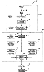
Fig. 2 illustrates the transmitter system 10' of
Fig. 1 incorporating a device consistent with the present
invention. Replacing the bandpass filter 20 of Fig. 1 is
the frequency verification circuit 30 of the present
invention. The frequency verification circuit 30
receives a modulated signal with an associated target
frequency from the exciter portion 32 of the transmission
system. The signal is received at a counter 34 in such a
manner as to reset the counter at the rising edge of a
cycle of the carrier signal. During each cycle, the
counter 34 is advanced by pulses from a high frequency
clock 36. The frequency of the clock 36 is intended to
_.5
CA 02440294 2003-09-09
be significantly higher than the frequency of the carrier
signal, generally around two orders of magnitude. Higher
or lower ratios between the two signals are also feasible
and are intended to be encompassed within the claimed
invention.
After the counter has been advanced for a full
cycle, the resulting count is retained and compared to
threshold values to determine if the signal is off-
frequency. Comparison values are stored within two
registers. The first reference register 38 contains a
value reflecting the number of cycles of the clock signal
that would occur in one cycle of a signal having a
predetermined frequency higher than that of the target
frequency. The second reference register 40 contains a
value reflecting the number of cycles of the clock signal
that would occur in one cycle of a signal having a
predetermined frequency lower than that of the target
frequency.
The count accumulated by the counter 34 is compared
to the first reference register 38 at a first comparison
portion 42. If the value of counter 34 exceeds that of
the first reference register 38, the carrier frequency is
smaller than a predetermined threshold frequency. The
first comparison portion 42 would thus produce an output
indicating that no error exists. If the value produced
at the counter 34 fails to exceed the value stored at the
first reference register 38, the first comparison portion
42 will produce an output indicating that the carrier
signal frequency is too high.
The value stored by the counter 34 is then compared
to the second reference register 40 at a second
-6 -
CA 02440294 2003-09-09
comparison portion 44. If the value of counter 34 is
below that of the second reference register 40, the
carrier frequency is larger than a predetermined
threshold frequency. The second comparison portion 44
would thus produce an output indicate that no error
exists. If the value produced at the counter 34 exceeds
the value stored at the second reference register 40, the
second comparison portion 44 will produce an output
indicating that the carrier signal frequency is too low.
The outputs of the first and second comparison
portions (42 and 44) are received an at error
determination portion 46. If either output indicates an
off-frequency carrier signal, the error determination
portion 46 determines whether it is necessary to
attenuate the carrier signal as a result of the frequency
deviation. This decision can be based upon the severity
of the deviation from the target frequency, the number of
cycles the deviation has continued, or any other relevant
factor. After this determination has been made, the
signal is passed to the amplifier 22 to be amplified and
transmitted at the antenna 24.
Fig. 3 is a flow diagram illustrating the run-time
operation of the present invention. The process 50
begins at step 52. The process then advances to step 54,
where the exciter produces a digital amplitude modulated
signal and inputs it to the frequency verification
circuit. At step 56, the system counts the number of
clock cycles of a high frequency clock that occur during
one cycle of the modulated carrier signal. The process
then continues at step 58, where this value is compared
to a first reference value. At step 60, the system
CA 02440294 2003-09-09
determines if the comparison between the two values
indicates an off-frequency carrier signal. For example,
the system may find a carrier signal to be outside of an
acceptable frequency range where the first reference
value is smaller than the number of counted clock cycles.
The process then continues at step 62, where the
number of counted clock cycles is compared to a second
reference value. At step 64, the system determines if
the comparison between the two values indicates an error.
For example, the system may find a carrier signal to be
outside of an acceptable frequency range where the second
reference value is larger than the number of counted
clock cycles.
If the modulated carrier signal is within an
acceptable range, the process continues to step 66, where
the carrier signal is amplified and transmitted. The
process then returns to step 52.
If an off-frequency signal is detected at either
comparison (steps 60 and 64), the process proceeds to
step 68, where the system determines if the off-frequency
signal creates an error condition. At this step, the
system will apply a decision rule by which the system can
determine if an error condition exists. For example, an
error condition may exist when a frequency deviation in
the carrier signal persists over a specified number of
carrier signal cycles. If no error condition is found,
the process advances to step 66, where the signal is
amplified and transmitted. If an error condition is
found, the process proceeds to step 70, where the signal
is attenuated. The process then advances to step 72,
where the system waits for an error reset signal. Once
-8-
CA 02440294 2003-09-09
this is received, the process returns to step 52 to
continue processing the incoming carrier signal.
In the example embodiment illustrated in Fig. 4, the
apparatus 100 monitors an AM carrier signal generated by
an IBOC (In-Band On-Channel) exciter and determines
whether the signal falls within five percent of a target
frequency. This is accomplished by counting the number
of 120 MHz clock pulses between rising edges of the AM
carrier signal and then comparing this count to a
programmable upper and lower limit. The carrier signal
is considered off-frequency where the count either
exceeds the upper limit or falls below the lower limit.
If the carrier signal is off-frequency, the system will
determine if it is necessary to attenuate the frequency.
Turning to the specifics of the illustrated
apparatus, a modulated carrier signal, with an associated
target carrier frequency, from the exciter 32 is received
at a synchronizer 102. The synchronizer 102 synchronizes
the received carrier signal with a clock signal provided
by a high frequency clock 104. Thus, a representation of
the carrier signal with approximately the same pulse
width as the original (within the width of one clock
cycle) and synchronous to the clock 104 is created. This
synchronized carrier is used to drive any component in
the apparatus that needs to use the AM carrier as an
input. The synchronized carrier is used to avoid
metastability issues that can occur with asynchronous
input signals.
The high frequency clock 104 provides a stable time
reference for the apparatus. In the example embodiment,
the clock signal is set at 120 MHz to give the signal
-9 -
CA 02440294 2003-09-09
sufficient resolution to measure a carrier wave of a
frequency up to 2 MHz. Each pulse from the clock 104
represents 1.60 of the period of this 2 MHz wave. Since
the AM band includes frequencies ranging from 1.65 MHz to
0.55 MHz, this signal provides good resolution throughout
the band of foreseeable carrier signals.
The clock signal and the AM carrier signal are both
inputted into a pulse generator 106. The pulse generator
106 provides a pulse of one clock cycle in width upon
detecting the rising edge of the AM carrier signal. This
rising edge marks the beginning of a carrier cycle. The
pulse from the pulse generator 106 is inputted to a
counter 108 to reset the counter and begin a count for a
new carrier cycle. Pulses from the clock 104 advance the
counter 108 in between reset pulses from the pulse
generator, measuring the number of clock cycle that pass
during each cycle of the AM carrier signal.
Upon the reception of a reset pulse from the pulse
generator 106, the number of clock cycles received in the
preceding carrier cycle is outputted from the counter 108
to a last count register 110. The last count register
110 stores the count for later analysis. This count is
passed to a pipeline register 112. The pipeline register
112 breaks the logic path of the circuit into two
portions, one to judge the lower bound of the frequency
of the modulated carrier signal and the other to judge
the upper bound of the frequency. While breaking the
logic path of the device into two shorter paths allows
the system to operate at the clock cycle frequency, it
introduces a latency of one clock cycle into the error
~ ~O -
CA 02440294 2003-09-09
determination of the system. This brief delay does not
significantly affect system performance.
The first of the outputs from the pipeline register
112 is provided to a first comparison portion 114. At
the first comparison portion 114, the count from the
pipeline register 112 is compared to a reference count
provided by a first reference register 116. In the
example embodiment, the count at the first reference
register 116 is supplied by an external microcomputer
(not shown) located in the exciter 32. This count is
established to reflect a frequency a set percentage
higher than that of an expected carrier signal. In the
example embodiment, the count contained in the first
reference register 116 reflects a frequency five percent
higher than the expected frequency associated with the
modulated carrier signal. Also in the example
embodiment, the first comparison portion 114 includes a
comparator 117 that outputs a logic "high" signal until
the count from the pipeline register 112 falls below the
count from the first reference register 116.
The second of the outputs from the pipeline register
110 signals is provided to a second comparison portion
118. At the second comparison portion 118, the count
from the pipeline register 112 is compared to a reference
count provided by a second reference register 120. In
the example embodiment, the count at the second reference
register 120 is supplied by an external microcomputer
(not shown) located in the exciter 32. This count is
established to reflect a frequency a set percentage lower
than that of an expected carrier signal. In the example
embodiment, the count contained in the second reference
CA 02440294 2003-09-09
register 116 reflects a frequency five percent lower than
the expected frequency associated with the modulated
carrier signal. Also in the example embodiment, the
second comparison portion 118 includes a comparator 121
that outputs a logic "high" signal until the count from
the pipeline register 112 exceeds the count from the
second reference register 120.
The outputs of the first and second comparison
portions (114 and 118) are outputted to the error
determination portion 122. Within the error detection
portion 122, the outputs are received at a logic device
124. The logic device 124 determines if the modulated
carrier signal frequency remains within the limits
recorded in the first and second reference registers (116
and 120). In the example embodiment, the logic device
124 includes an AND gate 125. The AND gate 125 will
receive logic "high" signals from the first and second
comparison portions (114 and 118) so long as the
frequency of the modulated carrier signal remains within
acceptable limits. Thus, the output of the AND gate 125
will remain a logic high until an off-frequency signal is
detected.
The digital filter 124 inhibits false alarms within
the system. Specifically, the digital filter 124
requires that an frequency deviation within the carrier
signal persist for a specified amount of time prior to
the system taking any action. Obviously, this time
period must be long enough to filter out common sources
of false alarms, but short enough to prevent damage to
the transmitter during the determination of the error
condition. It is known from observation of the IBOC
- I2-
CA 02440294 2003-09-09
digital waveform that instantaneous 180 degree phase
shifts or "phase reversals" are commonly present in the
IBOC digital waveform and make the frequency appear to
the detector to dramatically change instantaneously. The
so-called "phase reversal" causes a transition edge of
the digital signal to be missing for one cycle only. Twc
successive "phase reversals" never occur. These are
transient effects and should not be flagged as errors.
To account for these phase reversals in the example
embodiment, an off-frequency signal must be detected for
four cycles of the modulated carrier signal before the
system determined an error condition and attenuates the
off-frequency signal.
This error discrimination is accomplished by the
digital filter 126. The digital filter 126 receives
input both from the logic device 124 and the pulse
generator 106. When the digital filter 126 no longer
receives a logic "high" from the logic device 124, it
begins to count the pulses received from the pulse
generator 106. When three further pulses have been
received, the error condition has existed for four cycles
of the modulated carrier signal, and the digital filter
126 outputs a signal to an error latch 128 to disable the
transmission of the modulated carrier signal. Once the
error latch 128 is set to disable further transmission,
it remains in this state until reset through a control
register 130. The control register 130, like the first
and second reference registers (116 and 120), is directly
controlled by a microprocessor (not shown) found in the
exciter 32.
~('S_
CA 02440294 2003-09-09
It should be noted that in the preferred embodiment,
no error will be found when a carrier signal is not being
received by the system. The digital filter 124 will not
function to disable transmission of a carrier signal
unless it has received at least four pulses from the
pulse generator 108, indicating the passage of four
carrier signal cycles. These pulses will not be
generated in the absence of a signal. Additionally, if
the carrier is interrupted by other sources and then
later restored, no error will result since it is the time
between edges of the digital signal representing the
digital carriers that is important.
It will be understood that the above description of
the present invention is susceptible to various
modifications, changes and adaptations, and the same are
intended to be comprehended within the meaning and range
of equivalents of the appended claims. The presently
disclosed embodiments are considered in all respects to
be illustrative, and not restrictive. The scope of the
invention is indicated by the appended claims, rather
than the foregoing description, and all changes that come
within the meaning and range of equivalence thereof are
intended to be embraced therein.
-14-