Note: Descriptions are shown in the official language in which they were submitted.
CA 02440466 2003-09-10
WO 02/073302 PCT/IB02/00618
A liquid crystal display device
BACKGROUND OF THE INVENTION
1. Field of the Invention
The invention relates to a liquid crystal display device, and in particular to
a
liquid crystal display device that is constructed through a fabrication
process to apply a
sealant to either or both of two liquid crystal medium sandwiching substrates
for laminating
those two substrates through a given gap, and for adhering to and sealing
them, and then to
actually laminate the substrates.
2. Description of Related Art
In a fabrication process fox liquid crystal display panels, a sealant
consisting of
a material such as thermosetting resin paste is used as a material for bonding
two panel
substrates and for forming a chamber cell into which a liquid crystal material
is sealed
between the substrates. In general, a picture frame-like pattern of the
sealant is printed so as
to be located along the fringe of one of the substrates (in other words, so as
to surround a
display area keeping a given space to the display area). Then, this pattern-
formed sealant,
after some predetermined processes, is pressed against the other substrate and
cured through
a heating treatment so that a given gap (liquid crystal cell gap) is formed
between the
substrates in a substrate alignment process.
However, in these processes, there is a possibility of the sealant leaking or
flowing into the display area because the sealant is pressed against the
substrate in the
substrate alignment process and the sealant may be liquefied or softened in
the heating
treatment. If the sealant flows into the display area, pixel-forming elements
including a color
filter arranged correspondingly to the display area and pixel electrodes
connected to TFTs
might be covered with such flowing sealant or the quality of such elements
might be
deteriorated, which may further result in the so-called dot defect of the
displayed image.
One of the conventional countermeasures against such encroachment of the
sealant into the display area has been to provide a much sufficient distance
between the
pattern-formed sealant and the display area.
However, because of the recent tendency to expand the display area, a
(market) requirement that a distance between the sealant and the display area
should be
CA 02440466 2003-09-10
WO 02/073302 PCT/IB02/00618
2
shortened (the so-called narrow frame form) has been getting more and more
strong, and
therefore it cannot be allowed anymore to disregard the aforementioned problem
of the
sealant leakage into the sealant. Thus, it is a pressing need to provide a
technique for
preventing the leakage of the sealant into the display area when the
substrates are combined
even if the sealant has been put on closely to the display area.
SLT1VEVIARY OF THE INVENTION
From the aforementioned viewpoints, it is an object of the invention to
provide
a liquid crystal display device in which the leakage of the sealant into the
display area can be
very surely prevented.
In order to accomplish the object, a liquid crystal display device of one
aspect
according to the invention is a liquid crystal display device comprising: two
substrates in
which a display area is defined and which are overlaid with each other; at
least two dam
pattern structures being provided on at least one of the substrates or
provided separately on
both of the substrates, which have a pattern of surrounding the display area;
and a sealant
applied to the outside of the dam pattern structures in such a manner that the
sealant
surrounds the dam pattern structures, wherein the outer dam pattern structure
adjacent to the
sealant has a plurality of slits (for causing the sealant to pass
therethrough).
According to this aspect, the slits or gaps of the outer dam pattern structure
cause the sealant to easily pass through a passage and a space between the
inner dam pattern
structure and the outer dam pattern structure when the substrates are combined
and adhere to
each other. So, it is possible to suppress leaking out of the sealant into the
display area
beyond the inner dam pattern structure, that would be caused for some reason.
In the above mentioned aspect, any inner dam pattern structure of the dam
pattern structures except for the outer dam pattern structure may have a
pattern of
surrounding the display area in a generally continuous form.
Any inner dam pattern structure of the dam pattern structures except for the
outer dam pattern structure may have a plurality of slits for causing the
sealant to pass
therethough.
In the above mentioned aspect, the dam pattern structures may consist of three
dam pattern structures, and the innermost dam pattern structure thereof may
have a pattern of
surrounding the display area in a generally continuous form.
CA 02440466 2003-09-10
WO 02/073302 PCT/IB02/00618
3
Then the dam pattern structures may consist of three dam pattern structures,
and the central dam pattern structure thereof may have a pattern of
surrounding the display
area in a generally continuous form.
In order to achieve the above mentioned object, another aspect of liquid
crystal
display device according to the present invention is a liquid crystal display
device
comprising: two substrates in which a display area is defined and which are
overlaid with
each other; one or more dam pattern structures being provided on at least one
of the
substrates or provided separately on both of the substrates, which have a
pattern of
surrounding the display area; and a sealant applied to the outside of the darn
pattern
structures in a form of surrounding the dam pattern structures, wherein said
one or more dam
pattern structures comprise a dam pattern structure of column-shaped section
having a cross-
section connecting between mutually opposite faces of one and another of the
substrates.
Accordingly, the column-shaped section darn pattern structure completely
prevent the sealant from corning into the display area, so that the problems
previous
mentioned can be overcome. Furthermore, this aspect has an advantage that the
column-
shaped section dam pattern structure can determine a distance between the
substrates at a
fringe section of the substrates, whereby it will be useful for
control/setting of a thickness of
the liquid crystal cell.
In this aspect, the dam pattern structure of column-shaped section may have a
pattern of surrounding the display area in a generally continuous form.
The one or more dam pattern structures may comprise: an inner dam pattern
structure of column-shaped section having a cross-section connecting between
mutually
opposite faces of one and another of the substrates and having a pattern of
surrounding the
display area in a generally continuous form; and an outer daxn pattern
structure having a
plurality of slits (for causing the sealant to pass therethrough) and being
located on a side
close to the sealant.
Here, the outer dam pattern structure may have a column-shaped cross-section
connecting between mutually opposite faces of one and another of the
substrates.
Furthermore, the one or more dam pattern structures may comprise: an inner
dam pattern structure of column-shaped section having a cross-section
connecting between
mutually opposite faces of one and another of the substrates and having a
plurality of slits;
and an outer dam pattern structure of column-shaped section having a cross-
section
connecting between mutually opposite faces of one and another of the
substrates, having a
CA 02440466 2003-09-10
WO 02/073302 PCT/IB02/00618
4
plurality of slits (fox causing the sealant to pass therethrough) and being
located on a side
close to the sealant.
Preferably, intervals between the slits of the inner dam pattern structure of
column-shaped section are longer than those between the slits of the outer dam
pattern
structure of column-shaped section, and the slits of the inner dam pattern
structure of
column-shaped section do not correspond to the slits of the outer dam pattern
structure of
column-shaped section.
BRIEF DESCRIPTION OF THE DRAWINGS
Fig.l is a plan view of a liquid crystal display panel, which is for
explaining
the outline of dam pattern (structures) according to the invention.
Fig.2 is a partially enlarged plan view of a display panel, which
schematically
shows a form of dam patterns and a sealant according to the first embodiment
of the
invention.
Fig.3 is a cross-sectional view at A-A of Fig. 2 to explain the changing of
form
of the sealant after the process of combining the substrates and the effects
and advantages of
the invention.
Fig.4 is a partially enlarged plan view of a display panel, which
schematically
shows a form of dam patterns and a sealant after the process of combining the
substrates
according to the first embodiment of the invention.
Fig.S is a partially enlarged plan view of a display panel, which
schematically
shows a form of dam patterns and a sealant after the process of combining the
substrates
according to a comparative example.
Fig.6 is a partially enlarged plan view of a display panel, which
schematically
shows a form of darn patterns and a sealant according to the second embodiment
of the
invention.
Fig.7 is a cross-sectional view at B-B of Fig. 6 to explain the changing of
form
of the sealant and the effects and advantages of the invention.
Fig.8 is a partially enlarged plan view of a display panel, which
schematically
shows a form of a column-shaped section dam pattern and a sealant according to
the third
embodiment of the invention.
Fig.9 is a cross-sectional view at C-C of Fig. 8 to explain the changing of
form
of the sealant after the process of combining the substrates and the effects
and advantages of
the invention.
CA 02440466 2003-09-10
WO 02/073302 PCT/IB02/00618
Fig.lO is a partially enlarged plan view of a display panel, which
schematically shows a form of column-shaped section dam patterns and the
sealant according
to the forth embodiment of the invention.
Fig.l1 is a cross-sectional view at D-D of Fig. 10 to explain the changing of
5 form of the sealant after the process of combining the substrates and the
effects and
advantages of the invention.
DESCRIPTION OF THE PREFERRED EMBODI1VVIENT(S)
The aspects mentioned above and the other aspects of the present invention
will be described in more detail with reference to the accompanying drawings.
[Embodiment 1]
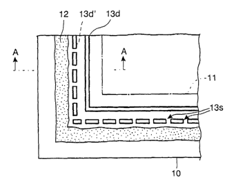
Fig. 1 shows in a plan view one of the panel substrates 10 to be used in one
embodiment of a liquid crystal display device according to the invention, Fig.
2 is an
enlarged view of the lower-left corner of Fig. 1, and Fig. 3 is an A-A cross
sectional view of
Fig. 2.
It should be noted that the one panel substrate 10 is combined with another
panel substrate 20 (see Figure 3) located opposite to the one panel substrate
10, and a liquid
crystal medium is sealed between those substrates to construct a final liquid
crystal display
device (panel). Besides, it is assumed that the one panel substrate 10 is a
substrate in which a
color filter is formed.
In Figs. 1-3, a given display area 11 is defined in the panel substrate 10 and
an
image to be displayed is formed within this display area 11. More
specifically, the display
area 11 in this example corresponds to an area in which the color filter
having a pattern of
color elements corresponding to color pixels is formed.
Around the display area 11, there are formed an inner dam pattern structure
13d adjacent to the display area 11 and an outer dam pattern structure 13d'
that is located
nearer to a side edge of the panel (a term "structure" will be omitted as
appropriate,
hereinafter), the dam patterns being separated at respective predetermined
distances from the
display area 11. The inner dam pattern 13d has a pattern of surrounding the
display area 11 in
a generally continuous form. On the other hand, although the outer dam pattern
13d'
surrounds the display area 11 in the outside of the dam pattern 13d in the
almost same
manner. However, the dam pattern 13d' is not continuous but has a pattern
including
discontinued portions 13s (referred to as "slits", hereinafter). Such slits
are only required to
CA 02440466 2003-09-10
WO 02/073302 PCT/IB02/00618
6
appear appropriately scattered when they are observed from a plan view, and in
this example
the slits are disposed with generally equal intervals (see Fig, 2).
The dam patterns 13d and 13d' can be formed in a layer of the same level as
the display area (color filter) 11 as illustrated in Fig. 3. As for material,
the dam patterns 13d
and 13d' can be formed from much the same material as used for the color
filter or from any
other materials including synthetic resins, pigments or metals. Prior to
coating of a sealant
12, the dam patterns 13d and 13d' are beforehand formed on the substrate 10
either along
with or separately from the color filter formation by means of, for example,
an etching
process.
The outside of the dam pattern 13d' is coated with the sealant 12 in such a
manner that-the sealant 12 surrounds the dam pattern 13d'. For the sealant 12
not only a
thermosetting resin as in this example may be used but also any UV setting
resins or any
other alternative materials.
Figs. 1 and 2 illustrate a state of the sealant 12 before a substrate
alignment
process. At this point, the sealant 12 still retains its pattern shape as it
has been printed.
Figs. 3 and 4 illustrate a state of the sealant 12 after the substrate
alignment
process. In Fig. 3, a sealant 12o is shown (by the broken line) which
represents its state just
after the pattern has been printed. When the sealant of such condition is
subjected to the
substrate combination (alignment) process wherein the substrate 10 is overlaid
with another
substrate 20, the sealant 12 will be pressed against the substrate 10 and be
forcedly
sandwiched between the substrates 10 and 20 so that the sealant 12 may be
extended in
directions parallel to the primary plane of the substrates (e.g. the left and
right directions in
Fig. 3). Then, the sealant 12 will be further softened and extended through
the subsequent
sealant heating process. As a result, the sealant 12 may not only extend
toward the outer
fringe of the panel but also flow out to a side of the inner dam pattern 13d
through the slits of
the outer darn pattern 13d'.
It should be particularly noted that the sealant 12 may easily flow into a
path
or a space 13p formed between the inner dam pattern 13d and easiness the outer
dam pattern
13d' through the slits 13s, and this easiness relies on the slit 13s which are
provided in the
outer dam pattern 13d'. In accordance with such structure, even if the sealant
12 is strongly
pressed during the substrate alignment process or it is liquefied or softened
eruptively during
the heating process, the sealant 12 may be prevented from flowing into the
display area 11
locally beyond the dam 13d for some reasons, as illustrated in Fig. 5 or by a
dash-doubledot
line 12, in Fig. 3.
CA 02440466 2003-09-10
WO 02/073302 PCT/IB02/00618
7
Thus, even if the sealant 12 is put on near to the display area 11, the
probability of leakage of the sealant 12 into the display area 11 can become
lower, so that it
is possible to finely expand the display area while the occurrence of the
aforementioned dot
defects is avoided.
It should be noted that Fig. 5 illustrates a structure in which an outer dam
pattern l3da comprises no slit.
[Embodiment 2]
Fig. 6 illustrates a schematic plan view of a structure of one panel
substrate,
dam patterns and a sealant formed on that substrate, which are used for a
liquid crystal
display device according to the other one embodiment of the invention. Fig. 7
illustrates a
cross sectional view from the B-B line of Fig. 6, where the substrates have
been combined
together.
In addition to the aforementioned darn patterns 13d, 13d', the dam patterns
illustrated in Figs. 6 and 7 further comprise a dam pattern 13d2 that is
disposed on the inner
side of the dam patterns 13d and 13d'. The inner dam pattern 13d2 is provided
to complement
the first embodiment and has a pattern of surrounding the display area in a
generally
continuous form in the same manner as for the inner dam pattern 13d. Also,
formation and
material of the dam pattern 13d2 are the same as the dam patterns 13d, 13d'.
According to this second embodiment, the extra dam pattern 13d2 is provided
so as to play a role as a stopper for damming off leakage of the sealant 12
beyond the dam
pattern 13d in case of accidental happening. By virtue of this structure, it
can be further
assured that the sealant 12 would be prevented from flowing into the display
area 11.
[Embodiment 3]
Fig. 8 illustrates a schematic plan view of a structure of one panel
substrate, a
dam pattern and a sealant formed on that substrate, which are used for a
liquid crystal display
device according to a further embodiment of the invention. Fig. 9 illustrates
a cross sectional
view from the C-C line of Fig. 7, where the substrates have been combined
together.
A dam pattern 13D in Figs. 8 and 9 is equivalent to the aforementioned dam
patterns 13d, 13d', l3da in that it has a cross section extending in a
direction perpendicular to
the primary plane of the substrate for blocking the sealant 12, but it is
different from them in
that it has a column-shaped cross-section connecting between mutually opposite
faces of one
and another of the substrates 10 and 20.
CA 02440466 2003-09-10
WO 02/073302 PCT/IB02/00618
Such a dam pattern 13D is completely engaged between the substrates to block
any stream of the sealant 12. Therefore, no leakage of the sealant 12 into the
display area
should occur.
However, the sealant 12 is usually considered to be fluid. So, if the dam
pattern 13D shuts between the substrates airtightly, during the substrate
alignment process
the air included in the sealant 12 cannot be easily exhausted in the vicinity
of the wall face of
the darn pattern whereby the cured sealant may have some air bubbles. In view
of this
respect, the following embodiment may be adopted.
[Embodiment 4]
Fig. 10 illustrates a schematic plan view of a structure of one panel
substrate,
dam patterns and a sealant formed on that substrate, which are used for a
liquid crystal
display device according to yet another embodiment of the invention. Fig. 11
illustrates a
schematic cross sectional view from the D-D line of Fig. 10, where the
substrates have been
combined together.
The dam patterns shown in Figs. 10 and 11 comprise an outer dam pattern
13D" having slits 13S" that have the same function as the slits 13s for the
aforementioned
dam pattern 13d' and an inner dam pattern 13D' having slits 13S' for
exhausting the air.
Each of these dam patterns 13D", 13D' has a cross-section connecting between
mutually
opposite faces of one and another of the substrates 10 and 20. In particular,
as shown in Fig.
10, the slits 13S' of the dam pattern 13D' and the slits 13S" of the dam
pattern 13D" are
positioned so as not to correspond to each other. Furthermore, in this
example, the intervals
between the slits 13S" are set to be longer than those between the slits 13S'.
By virtue of such structure, the sealant could more easily pass through the
slits
13S" of the outer dam pattern 13D", and accordingly the air could be more
easily exhausted,
so that the generation of the air bubbles as mentioned above can be prevented
in the finished
product.
[Variations]
Although in the above embodiments it has been assumed that one of the
substrates is a panel substrate (front substrate) in which the color filter
has been formed, the
dam patterns shown in the Embodiments 1-4 may be disposed on another substrate
opposite
to the front substrate (rear substrate in which, for example, thin film
transistors for driving
pixels are formed). Also, the coating of the sealant 12 on the front substrate
is not limited.
Instead, the sealant 12 may be put on only the rear substrate, and may be put
on both
substrates.
CA 02440466 2003-09-10
WO 02/073302 PCT/IB02/00618
9
Moreover, such dam patterns as shown in the Embodiments 1 and 2 may be
applied to both of the front and rear substrates. In this case, the effect of
preventing the
leakage of the sealant into the display area could be more enhanced. Also, it
is a matter of
course that each of such dam patterns as shown in the Embodiments 1, 2 and 4
may be
individually applied to either front substrate or rear substrate, as
appropriate.
Besides, although the number of the dam patterns shown in the
aforementioned embodiments has been one to three, any number of the dam
patterns may be
applicable to the invention. The invention essentially aims to provide a
constitution with
certain contrivance for preventing the leakage of the sealant into the display
area. Therefore,
it should be noted that the concept of the invention is not to focus on the
number of the dam
patterns but to prevent unexpected local flow of the sealant into the display
area. And to this
end, it is proposed to provide slits to the dam pattern located relatively
near to the sealant side
in the case of two or more fence-like cross-section darn patterns having cross
sections that
extend in a direction perpendicular to a main surface of the substrate
terminating at an
intermediate position between the substrates, or to provide a dam pattern
itself having a
column-shaped section connecting between mutually opposite faces of one and
another of the
substrates.
Furthermore, in the Embodiments 1 and 2, only purport based on a
combination of the intermittent dam pattern with some slits and the continuous
dam pattern
without any slits has been introduced, but, in accordance with purport based
on the
embodiment of Fig. 10, another combination in which only intermittent dam
patterns are
combined may be possible.
Nothing to say, any other various variations may be implemented in the
invention. For example, the sealant may comprise an ultraviolet curing
(setting) resin, and the
invention may be applicable to any other substrates in which the color filter
and the display
area are not matched each other.
Furthermore, although this specification has descriptions that the sealant
talces
a shape surrounding the display area at its application stage, the cured
sealant, in fact, is
usually a frame-shaped pattern having some opening portion for implanting the
liquid crystal
medium. This specification does not refer to this respect for the
simplification purpose. In
addition, such dam patterns as mentioned in the Embodiments 3 and 4 have to
make
allowances for such implantation of the liquid crystal material, but in these
embodiments the
corresponding description also has been omitted.
CA 02440466 2003-09-10
WO 02/073302 PCT/IB02/00618
The preferred embodiments described herein are therefore illustrative and not
restrictive, the scope of the invention being indicated by the appended claims
and all
variations which come within the meaning of the claims are intended to be
embraced therein.