Note: Descriptions are shown in the official language in which they were submitted.
CA 02440694 2003-09-11
WO 02/073322 PCT/US02/07486
QUASI-CW DIODE-PUMPED, SOLID-STATE UV LASER SYSTEM
AND METHOD EMPLOYING SAME
Related Applications
[0001] This patent application derives priority from U.S. Provisional Patent
Application
No. 60/275,246, filed March 12, 2001.
Copyright Notice
[0002] ~ 2001 Electro Scientific Industries, Inc. A portion of the disclosure
of this
patent document contains material which is subject to copyright protection.
The copyright
owner has no objection to the facsimile reproduction by anyone of the patent
document or
the patent disclosure, as it appears in the Patent and Trademark Office patent
file or
records, but otherwise reserves all copyright rights whatsoever. 37 CFR ~
1.71(d).
Technical Field
[0003] This invention relates to diode-pumped, solid-state lasers and, in
particular, to
quasi-CW diode-pumped UV laser systems and processing methods employing them,
such
as for forming vies in circuit boards.
Background of the Invention .
[0004] Different types of lasers systems have been employed to drill vies at
point-to-
point target areas on electronic devices or work pieces such as printed
circuit boards
(PCBs). The following discussion is presented herein only by way of example to
diode-
pumped, solid-state ultraviolet (UV) laser systems and work piece targets and
should not
be considered limiting to the scope of invention.
[0005] When an acousto-optically (A-O) Q-switched, continuous-wave (CW)' diode-
pumped (DP), solid-state (SS) laser system, such as Electro Scientific
Industries, Inc.'s
(ESI) Model 5200 which includes a Light Wave Electronics' (LWE) Model 210
laser, is
employed to create vies, the pumping diode or diodes remain active
continuously. Laser
1
CA 02440694 2003-09-11
WO 02/073322 PCT/US02/07486
emission is prevented by closing the Q-switch whenever the positioning system
is directed
to a new target area on the work piece. After the positioning system is
aligned to the new
target area, the laser system delivers .a laser output containing one or more
laser pulses by
opening the Q-switch at a predetermined repetition rate.
[0006] The LWE Model 210 employs two 20 Watt (W) CW-diodes for pumping and
generates 3 W of UV output power at 10 kHz repetition rate. The CW pumping
current to
the diodes is limited by thermal loading of the diodes. If an application
warrants greater
UV output power, then either more diodes or diodes with higher current/power
must be
employed, such as two 30 W diode laser bars or four 20 W diode laser bars.
About 8 W of
UV output power can be expected from such designs. However, if higher pumping
power
is employed, thermal loading on the solid-state laser medium is increased.
Thermally
overloading the laser medium can permanently damage it or cause significant
degradation
of the laser beam quality and limit the power available. This limitation
imposes a critical
engineering challenge to the laser system design and manufacturing.
[0007] Other pumping schemes are, however, available for a laser design, such
as pulse
pumping and quasi-CW pumping. An electro-optically (E-O) Q-switched pulsed
DPSS UV
laser, such as early versions of Lambda Physics' UV "Gator" Model, provide
higher laser
pulse power but at low pulse repetition rates. For each pumping pulse, only
one UV laser
pulse is generated. The pumping duration time is limited to a few hundred
microseconds
(,us) so the laser output pulse repetition rate is typically limited to below
2 kHz. This
pumping scheme is not preferred for drilling vias because it adversely affects
drilling
throughput.
[0008] Traditional quasi-CW pumping resembles pulse pumping but exhibits
longer
pumping duration time at a lower peak pumping power. The pumping scheme can
exhibit a
pumping repetition rate of about 1-2 kHz, and the pumping duration time can be
from a few
hundred ~s to a few milliseconds (ms), based on the repetition rate and the
duty cycle of the
diodes used. This pumping scheme allows pumping to a higher level than does CW
pumping because the diode "rests" (and thermal loading reduces or stops)
whenever the
pumping is off. Therefore, the laser output power can be higher during the
pumping time
period compared to that of a comparable CW pumped laser. The laser output is
controlled
by regulating the current to the diode(s). The pumping repetition rate of this
pumping
scheme is, however, still a serious drawback. Typical applications for quasi-
CW pumping
2
CA 02440694 2003-09-11
WO 02/073322 PCT/US02/07486
include those that utilize a long laser pulse width and a modest peak power,
such as laser
bonding and welding.
[0009] A laser system that includes a pumping scheme that facilitates both
higher power
and a faster repetition rate to increase drilling throughput is therefore
desirable.
Summary of the Invention
[0010] Conventional UV laser via drilling systems employ a standard frequency
conversion scheme to convert the laser's fundamental wavelength in the IR
region to the
UV. Such systems preferably employ high UV power and a high pulse repetition
rate to
achieve high throughput via formation, hence A-O, Q-switched DPSS laser
systems have
heretofore been preferred for drilling vias.
[0011] A commercially desirable system would prefer higher UV power for
reducing
the via drill time, or to make acceptable vias on some "hard to drill"
materials, such as
copper and FR4. Thus, a high UV output power (5 to 15 W) at a high pulse
repetition rate
(a few kHz to a few tens kHz) would be preferred.
[0012] Also to be commercially useful, via formation on PCBs, for example,
demands a
laser system to be capable of making 300 to 400 vias per second. Thus, the
laser
positioning system has to move to 300 to 400 new locations every second.
Typically, it
takes the laser system less than one ms to drill one via, but in some cases
longer than one
ms to move to a new location for a next via. Hence, the time for the laser
being ON is
actually less than the time the laser is being OFF, which makes the use of the
laser quite
inefficient.
[0013] The present invention provides a quasi-CW diode- or lamp-pumped, A-O, Q-
switched solid-state UV laser that synchronizes the timing of the quasi-CW
pumping to
avoid or reduce pumping while the positioning system is moving from one target
area to the
next target area and to increase the pumping level beyond the CW pumped level
while
drilling vias. Thus, the available UV power for via formation is higher even
though the
average pumping power to the laser medium, and thermal loading of the pumping
diodes,
remains the same as for conventional CW pumping with conventionally available
laser
diodes. The quasi-CW pumping current profile can be further modified to
realize a
preferred UV pulse amplitude profile.
3
CA 02440694 2003-09-11
WO 02/073322 PCT/US02/07486
[0014] Such a quasi-CW diode- or lamp-pumped, A-O Q-switched, solid-state UV
laser
is new; the synchronization of the quasi-CW pumping with the beam scanning is
new; and
the usage of such a laser system for via formation is new.
[0015] Additional objects and advantages of this invention will be apparent
from the
following detailed description of preferred embodiments thereof which proceeds
with
reference to the accompanying drawings.
Brief Description of the Drawings
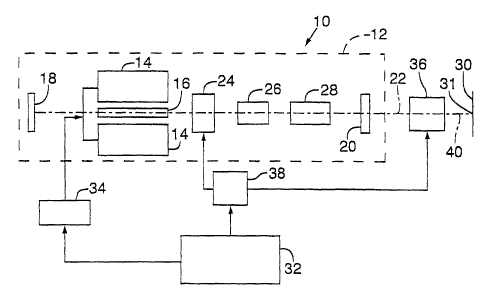
[0016] FIG. 1 is a simplified schematic diagram of one embodiment of a quasi-
CW
diode-pumped, A-O Q-switched laser with infra-cavity tripling frequency
conversion.
[0017] FIG. 2A is a simplified graphical depiction of an exemplary waveform of
quasi-
CW pumping diode current.
[0018] FIG. 2B is a simplified graphical depiction of exemplary A-O Q-switched
laser
pulses superimposed on the quasi-pumping diode current shown in FIG. 2A.
Detailed Description of Preferred Embodiments
[0019] FIG. 1 is a simplified schematic diagram of a preferred embodiment of a
quasi-
CW, diode-pumped, A-O Q-switched, solid-state UV laser system 10 with
synchronized
targeting, pumping, and firing to form vias at a high throughput rate. With
reference to
FIG 1, laser resonator 12 of laser system 10 is shown with diodes 14 pumping
laser
medium 16 from the side. Skilled persons will appreciate, however, that the
resonator 12
can fold and that the pumping scheme can be "end pumping" or that laser system
10 could
employ other possible well-known configurations. Exemplary diodes 14 include,
but are
not limited to, Models SDL-3200 series 100 W quasi-CW arrays and 960 W high-
duty
factor stacked arrays sold by SDL, Inc. of San Jose, California. Exemplary
solid-state
laser mediums (16) include laser mediums having YAG, YLF, and YVOa.
compositions.
Between an IR-reflective mirror 1~ and UV (third harmonic)-transmissive output
coupler
20, resonator 12 also includes, along its optic axis 22, an acousto-optic (A-
O) Q-switch 24,
a frequency doubler 26, and a frequency tripler 28 for infra-cavity frequency
conversion.
Skilled persons will appreciate that frequency conversion can be accomplished
externally to
resonator 12.
[0020] FIGS. 2A and 2B (collectively FIG. 2) are respective simplified
graphical
depictions of an exemplary waveform of quasi-CW-pumping diode current pulses
or
intervals SOa, SOb, and SOc (generically current intervals 50) and of
exemplary A-O Q-
4
CA 02440694 2003-09-11
WO 02/073322 PCT/US02/07486
switched laser pulses 60a, 60b, and 60c (generically laser pulses 60)
superimposed on the
quasi-CW-pumping diode current waveform shown in FIG. 2A. With reference to
FIGS. 1
and 2, laser system operation is synchronized such that when the laser system
10 finishes
making one via at a first target area 31 on work piece 30, the central
processing unit (CPU)
32 stops the diode pumping (turns the diode current to zero) or reduces the
diode pumping
to a pre-determined low current level by controlling power supply 34.
Exemplary power
supplies 34 include, but are not limited to, Model SDL-820, for 10-15 amp CW
laser diode
driver with typical 10 ~,s current transition time; Model SDL-830 for about 50
amp CW
laser driver; or Model SDL-928, for about 150 amp peak quasi-CW laser diode
array
drivers. All sold by SDL, Inc. of San Jose, California.
[0021] Then, positioning system 36 moves the beam output position to a new
target area
31. The beam positioning system 36 preferably includes a translation stage
positioner that
employs at least two transverse stages permitting quick movement between
target areas 31
on the same or different work pieces 30. In a preferred embodiment, the
translation stage
positioner is a split-axis system where a Y stage moves work piece 30, and an
X stage
moves a fast beam positioner and associated focusing lens(es). The Z dimension
between
the X stage and Y stage may also be adjustable. The positioning mirrors align
the optical
path 22 through any turns between laser resonator 12 and the fast beam
positioner. The
fast beam positioner may for example employ high resolution linear motors
and/or a pair of
galvanometer mirrors that can conduct unique or repetitive processing
operations based on
provided test or design data. The stages and positioner can be controlled and
moved
independently or coordinated to move together.
[0022] Beam positioning system 36 can employ conventional vision or beam to
work
alignment systems that work through an objective lens or off axis with a
separate camera
and that are well known to skilled practitioners. In one embodiment, an HRVX
vision box
employing Freedom Library software in a positioning system 36 sold by Electro
Scientific
Industries, Inc. is employed to perform alignment between the laser resonator
12 and the
target areas 31 on the work piece 30. Other suitable alignment systems are
commercially
available.
[0023] In addition, beam positioning system 36 also preferably employs non-
contact,
small-displacement sensors to determine Abbe errors due to the pitch, yaw, or
roll of the
stages that are not indicated by an on-axis position indicator, such as a
linear scale encoder
CA 02440694 2003-09-11
WO 02/073322 PCT/US02/07486
or laser interferometer. The Abbe error correction system can be calibrated
against a
precise reference standard so the corrections depend only on sensing small
changes in the
sensor readings and not on absolute accuracy of the sensor readings. Such an
Abbe error
correction system is described in detail in International Publication No. WO
01/52004 A1
published on July 19, 2001 and U.S. Publication No. 2001-0029674 A1 published
on
October 18, 2001. The relevant portions of the disclosure of the corresponding
U.S. Pat.
Appl. No. 09/755,950 of Cutler are herein incorporated by reference.
[0024] Many variations of positioning systems 36 are well known to skilled
practitioners and some embodiments of positioning system 36 are described in
detail in
U.S. Pat. No. 5,751,585 of Cutler et al. The ESI Model 5320 microvia drilling
system
available from Electro Scientific Industries, Inc. of Portland, Oregon is a
preferred
implementation of positioning system 36 and has been used for laser drilling
of resin coated
copper packages for the electronics industry. Other preferred positioning
systems such as
Model series numbers 27xx, 43xx, 44xx, or 53xx, manufactured by Electro
Scientific
Industries, Inc. in Portland, Oregon, can also be employed. Skilled persons
will also
appreciate that a system with a single X-Y stage for work piece positioning
with a fixed
beam position and/or stationary galvanometer for beam positioning may
alternatively be
employed. Those skilled in the art will recognize that such a system can be
programmed to
utilize toolpath files that will dynamically position at high speeds the
focused UV laser
system output pulses 40 to produce a wide variety of useful patterns, which
may be either
periodic or non-periodic.
[0025] The CPU 32 causes current to be applied or increased to the diodes 14
either
when the positioning system 36 reaches, or is about to reach, a new or second
target area
31 or at a predetermined time interval following and inhibition or reduction
in diode
pumping. The CPU 32 instructs the Q-switch control 38 to open the Q-switch 24
to deliver
the laser pulses 60 at a predetermined repetition rate until the second via is
made.
[0026] The profile of the pumping current.intervals 50 can be modulated to
control the
shape of the peak power profile of the laser pulses 60 during the quasi-CW
pumping, such
as flat, from low to high (shown in FIG. 2A) or from high to low during the
period.
Furthermore, the current profiles can be modulated to have different
amplitudes so for
example a high peak power can be used for drilling metal layers and lower peak
power can
be used for drilling dielectric layers, if desired. Similarly, the time
periods for current
6
CA 02440694 2003-09-11
WO 02/073322 PCT/US02/07486
pumping intervals 50 can be adjusted to suit the size, depth, and material of
the via to be
processed, such as longer current intervals 50 for larger diameter vias. FIG.
2A and 2B
demonstrate that the laser system 10 permits, but does not require, variable
periods of
current pumping intervals 50 and variable periods between current pumping
intervals 50,
while the duty cycle can be kept the same. The duty cycle could, however, be
varied as
well, if desirable for laser output profiling.
[0027] The quasi-CW pumping repetition rate can easily be made as high as 2
kHz.
The interval time between the quasi-CW pumping doesn't have to be constant as
long as the
average thermal loading to the laser. pumping diode 14 and/or laser medium 16
remains
relatively constant or below thermal damage levels.
[0028] In one embodiment, the diodes 14 and power supply 34 of a CW pumped 5 W
UV laser system 10 are changed to be conducive to variable current pumping.
The
resulting laser system 10 is able to run at a duty cycle of 2 to 1 at 500 Hz.
The diodes 14
pump the laser medium 16 fox 1 ms before they stop for another 1 ms. Thus,
during the
pumping period, about twice as much current can be put into the diodes 14
(without
adversely affecting the average thermal loading on the diodes 14 or the laser
medium 16).
Thus, the laser power during that 1 ms pumping period can be more than twice
as much as
that from a comparable CW pumped laser (especially after the nonlinear
frequency
conversion). The A-O Q-switch 24 used in the laser resonator 12 repetitively
switches to
deliver the laser pulses 60 at a pre-determined repetition rate of, for
instance, 10 kHz or up
to 50 kHz. ,
[0029] Work piece 30 that may, for example, be an IC chip package, MCM,
capacitor,
circuit board, resistor, or hybrid or semiconductor microcircuit. For
convenience, work
piece 30 is described below as only having four layers. Top and bottom
conductive layers
may contain, for example, standard metals such as, aluminum, copper, gold,
molybdenum,
nickel, palladium, platinum, silver, titanium, tungsten, metal nitrides, or
combinations
thereof. Conventional metal layers vary in thickness, typically between 9-36
,um, but may
be thinner or thicker. The conductive layers are typically made of the same
material.
[0030] A dielectric matrix or layer is sandwiched between the conductive
layers and
may, for example, contain a standard organic dielectric material such as
benzocyclobutane
(BCB), bismaleimide triazine (BT), cardboard, cyanate esters, epoxies,
phenolics,
polyimides, polytetrafluorethylene (PTFE), various polymer alloys, or
combinations
7
CA 02440694 2003-09-11
WO 02/073322 PCT/US02/07486
thereof. Conventional organic dielectric layers vary considerably in
thickness, but are
typically much thicker than the metal layers. An exemplary thickness range for
organic
dielectric layers is about 30-400 ~,m.
[0031] The dielectric layer may also contain a standard reinforcement
component that
may include a fiber matte or dispersed particles of, for example, aramid
fibers, ceramics,
or glass woven or dispersed throughout the organic dielectric. Conventional
reinforcement
components are typically individual filaments or particles of about 1-10 ,um
in size and/or
woven bundles of 10 ,um to several hundreds of microns. Skilled persons will
appreciate
that reinforcement components may be introduced as powders into the organic
dielectrics
and can be noncontiguous and nonuniform. Such composite or reinforced
dielectric layers
typically require laser processing at a higher fluence than is needed to
ablate unreinforced
dielectric layers. Skilled persons will also appreciate that these various
layers may also be
internally noncontiguous, nonuniform, and nonlevel. Stacks, having several
layers of
metal, dielectric, and reinforcement material, may be thicker than 2 mm.
[0032] Via diameters preferably range from 25-300 gum, but laser system 10 may
produce vies that have diameters as small as about 5-25 ,um or greater than 1
mm. Because
the preferred ablated spot size of laser pulses 60 is about 25-75 ~,m in
diameter, vies larger
than 25 ,um may be produced by trepanning, concentric circle processing, or
spiral
processing. Skilled persons will appreciate that vies may be noncircular, such
as square,
rectangular, oval, slot-like, or other surface geometries.
[0033] Through-hole vies cleanly and evenly penetrate all layers and materials
of work
piece 30 and preferably exhibit negligible taper from via fop to via bottom.
Blind vies do
not penetrate all layers and/or materials, typically stopping at a lower or
bottom conductive
layer. Proper selection of the laser parameters permits the lower or bottom
conductive
layer to remain unaffected even if it comprises the same metal components) as
the top
metal layer.
The parameters of laser output 40 are selected to facilitate substantially
clean,
sequential drilling, i.e., via formation, in a wide variety of metallic,
dielectric, and other
material targets that may exhibit different optical absorption, ablation
threshold, or other
characteristics in response to UV or visible light. The parameters of laser
system output 40
include an average energy per pulse greater than about 120 ,u,T measured at
the work
surface, preferably greater than 200 ,u,T; spot size diameters or spatial
major axes of less
8
CA 02440694 2003-09-11
WO 02/073322 PCT/US02/07486
than about 50 ,um, and preferably from about 1-50 ~,m; a repetition rate of
greater than
about 1 kHz, preferably greater than about 5 kHz, and most preferably even
higher than 20
kHz; and a wavelength preferably between about 190-532 nm, and most preferably
between
about 250 nm and 400 nm. Specific preferred wavelengths include, but are not
limited to,
1064 nm, 532 nm, 355 nm, 349 nm, or 266 nm.
[0034] The preferred parameters of laser output 40 are selected in an attempt
to
circumvent certain thermal damage effects by utilizing temporal pulse widths
that are
shorter than about 150 ns, and preferably from about 40-90 ns or lower.
Skilled persons
will also appreciate that the spot area of laser pulses 60 is generally
circular, but may be
slightly elliptical. Preferred UV laser drilling parameters are disclosed in
U.S. Patent Nos.
5,593,606 and 5,841,099.
[0035] Blind vies, and particularly blind vies with large diameters, are
preferably
created by a two pass process in which the conductive layer for all target
areas is removed
in the first pass and then the dielectric layer for all the target areas is
removed during the
second pass with the fluence of the laser output being below the conductive
layer ablation
threshold. After the top conductive layer of all the target areas is removed,
the fluence for
the laser output during the second pass can be reduced by defocusing the laser
spot and/or
by increasing the repetition rate, as well as by decreasing the current to the
laser pumping
diode 14.
[0036] Skilled persons will appreciate that blind vies can also be created in
a single pass
process where both the conductive and dielectric layers of each target are is
removed before
the positioning system 36 moves to a subsequent target area 31. Single pass
processing is
preferred for creating smaller diameter vies. In a single pass process, it
would be more
efficient to maintain a fairly high fluence as the laser pulses 60 begin to
remove the
dielectric layer, but as the laser pulses 60 clear away the dielectric layer
and expose the
bottom conductive layer such that it begins to absorb heat from laser output
40, damage to
the bottom conductive layer would be reduced by using a lower fluence. Thus, a
gradual
defocus of the laser spot or decrease in the pumping current during dielectric
removal
would be faster, more efficient, and protect bottom metal layer better than
using a single
fluence for dielectric removal. These and other laser output profiling
techniques for via
drilling processes are described in detail in U.S. Patent Application No.
09/823,922 and
U.S. Patent Publication No. US2001-0045419, published on November 29, 2001.
The
9
CA 02440694 2003-09-11
WO 02/073322 PCT/US02/07486
detailed description and drawings of U.S. Patent Application No. 09/823,922
are herein
incorporated by reference.
[0037] It will be obvious to those having skill in the art that many changes
may be made
to the details of the above-described embodiment of this invention without
departing from
the underlying principles thereof. ~ The scope of the present invention
should, therefore, be
determined only by the following claims.