Note: Descriptions are shown in the official language in which they were submitted.
CA 02440700 2003-09-05
WO 02/073832 PCT/US02/00122
-1-
CREDIT CARD COMMUNICATION SYSTEM
STATEMENT RE: FEDERALLY SPONSORED RESEARCH/DEVELOPMENT
(Not Applicable)
BACKGROUND OF THE INVENTION
The present invention relates generally to
communications systems, and more particularly to a
miniaturized communications system.
Miniaturization of commercial communications systems
has focused upon the use of micro-cellular architectures,
such as the one shown in Figure 1 which employs one high
power base station transmitter 20 to communicate to remote
communication devices 22 and many micro-cell receivers.
Given that the remote communication devices only radiate a
low power radio frequency (RF) signal, many receivers are
required to encompass the area of the high power
transmitter. Given the multitude of receivers required,
the micro-cellular architecture is costly. Due to the fluid
and ever-changing military battle space, traditional
commercial communication systems are unsuitable for
military deployment.
Thus, a need exists for a miniaturized communication
system with an architecture suitable for military
deployment. Preferably, the architecture includes one base
station which can be located in an aircraft (manned or
unmanned) or atop a tower.
BRIEF SUMMARY OF THE INVENTION
A system for communications is disclosed. The system
includes a base station and wireless long-range
communication devices which are approximately the size of
a credit card.
Preferably, the base station includes a high
temperature superconductivity receiver.
In accordance with other aspects of the invention, the
wireless communication devices each include a transceiver,
CA 02440700 2003-09-05
WO 02/073832 PCT/US02/00122
-2-
a man machine interface, a processor, a power supply and an
antenna.
In accordance with still other aspects of the
invention, preferably, the transceiver includes a frequency
shift keying receiver. Preferably, the transceiver
includes a direct sequence spread spectrum modulator with
differential phase shift keying.
In accordance with yet other aspects of the invention;
the man machine interface includes a display. Preferably,
the display is a thin polymer emissive display that is
capable of displaying both graphical and textual
information. Preferably, the man machine interface
includes pushbuttons (e.g., four pushbuttons).
In accordance with further aspects of the invention
the power supply includes a battery. Preferably, the
battery is a primary lithium non-rechargeable battery or
a secondary lithium polymer rechargeable battery.
Preferably, the power supply also includes a constant
current source charger and a low dropout analog regulator.
In accordance with still further aspects of the
invention, the antenna is either a monopole antenna, a
dipole antenna, or a patch antenna.
In accordance with yet further aspects of the
invention, the communications system is a voice response
architecture and includes a microphone. Preferably, the
voice response architecture also includes an integrated
broadband processor.
BRIEF DESCRIPTION OF THE DRAWINGS
These as well as other features of the present
invention will become more apparent upon reference to the
drawings wherein:
Figure 1 is a diagram of an exemplary prior art
commercial micro-cellular architecture;
Figure 2 is a diagram of an exemplary architecture
formed in accordance with the present invention;
Figure 3 is an exemplary configuration of the credit
card communications system of the present invention;
CA 02440700 2003-09-05
WO 02/073832 PCT/US02/00122
-3-
Figure 4 is a block diagram of an exemplary
architecture of a credit card communication system of the
present invention;
Figure 5 is a block diagram of an alternative (voice
response) architecture of a communication system of the
present invention;
Figure 6 illustrates exemplary antenna configurations
suitable for use in an exemplary architecture for the
present invention;
Figure 7 illustrates the assignment of a unique slot
in a master frame via a hashing function;
Figure 8 illustrates how adaptive sleep eliminates
variation in resistor capacitor (RC) oscillator frequency
due to process and temperature changes;
Figure 9 is an exemplary communications state diagram;
and
Figure 10 is an illustration of a forward/reverse
channel frame format.
DETAILED DESCRIPTION OF THE INVENTION
The exemplary architecture of the present invention
shown in Figure 2 is a network architecture which includes
a single high power base station 20 which communicates with
credit card size wireless communications devices. Thus, the
invention is referred to as a Credit Card Communications
System (C3S) herein. Due to the single base station (or
interrogator) architecture, the C3S system is capable of
quick setup and mobility which can accommodate battle field
operations. While ideally suited for military operations,
it will be appreciated that the present invention is not so
limited. For example, the invention has commercial uses,
such as a credit card sized pager, preferably with smart
card capabilities. The invention can also be used as a
reduced function device which serves as a low cost long-
range active radio frequency identification device (RFID).
For example, several of the credit card sized communication
devices can be put on several sides of a pallet or
container. Traditional RFIDs are much more costly than the
CA 02440700 2004-01-15
4
credit card sized communication device of the present
invention because smart card form factor devices can be
mass produced (for example, using reel-to-reel
processing). The credit card communication system of the
present invention can communicate with a Global
Positioning System (GPS) such that the credit card
communications device can receive its location and can
then upload its location to the base station. Another
application of the present invention is for the credit
card communications device to receive information which
includes a phone number. The card is then inserted into
a phone and the phone number is automatically dialed. It
will be appreciated that the above examples illustrate a
few possible applications of the credit card
communications system of the present invention and that
many other applications are possible.
As illustrated in Figure 2, the C3S utilizes a
single high power forward channel transmitter 30.
Because the communicator of the C3S uses a simple
receiver due to the aggressive size constraints,
preferably, FSK modulation is utilized. In exemplary
embodiments, the C3S employs high temperature
superconductivity technology and spread spectrum coding
to improve base sensitivity which eliminates the need for
multiple micro-cellular receivers. Due to the enhanced
base station, the C3S communicator's radio frequency
output power is very low which increases battery life and
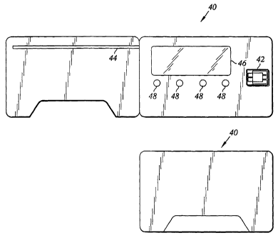
enables using a small planar battery. Figure 3
illustrates an exemplary configuration of the C3S credit
card 40. The packaging of the credit card 40 is a smart
card form factor (e.g., approximately 9.6 cm x 6.4 cm
with a thickness of .79 mm) and includes a complex
transceiver 42, an antenna 44 and a man machine interface
(MMI). Preferably, the communicator's MMI includes a
display 46, such as a dot matrix display, push buttons 48
and a microphone (not shown). Although a srnart card form
factor is preferable, it will be appreciated that other
configurations can be used, for example, the card can be
a magnetic stripe card.
CA 02440700 2003-09-05
WO 02/073832 PCT/US02/00122
-5-
Text or graphical information is delivered to the
communicator, for example, via a forward channel frequency
shift keying (FSK). The user can communicate with the base
station (e.g., using predetermined responses and/or
compressed voice) via, for example, the direct sequence
spread spectrum (DSSS), phase shift keying (PSK) reverse
channel. Preferably, the C3S single base station
architecture of the invention is predicated upon a forward
channel high power base station and an optimized reverse
channel. The architecture combines various technologies,
for example, DSSS, a high temperature superconductivity
receiver, and an adaptive base station antenna array.
Together these technologies allow a low power C3S
transmitter to communicate with the base station with an
acceptably low error rate.
Preferably, the invention employs DSSS reverse channel
in order to improve interrogator sensitivity and to reject
unwanted signals. Due to the nature of DSSS communications,
when transmissions from remote transmitters are correlated,
interfering signals are de-correlated. This allows for
rejecting of unwanted signals that are not strong enough to
overload the receiver's low noise amplifier (LNA).
The sensitivity of the interrogator is a function of
temperature and bandwidth. For a DSSS based link, the
bandwidth is the coherent bandwidth for the focused code.
Preferably, the C3S utilizes a focused code bandwidth of
1000 hertz and a temperature of 77 degrees Kelvin.
An adaptive interrogator antenna array helps reject
unwanted signals because unwanted signals which are not
located at the same geolocation as wanted signals can be
rejected by use of a sectored gain antenna array or an
adaptive sectored gain antenna array. The adaptive
sectored antenna array subtracts the unwanted signal from
the wanted signal thus canceling the unwanted signal.
The sensitivity of a receiver is defined primarily by
its noise figure and noise power. High temperature
superconductivity (HTS) allows the LNA and front end power
filter RF components to be constructed such that a noise
~ . _ ~ A , O ~ ~
CA 02440700 2003-09-05 P~~~
'(7,~
A-2328/424PC LJ.
D.
(~;;;! (i,... 11 õ il ; I il, i ~~_.ii 1CC~ . ~{..i{ {1...i~ .'il " :It ' ;,1i
= f if, ~~ tl'~':'.li "'.1t I !
-6-
figure of less than 0.5 dB can be realized. In addition,
noise power is set by the system's temperature and
bandwidth. Thus, the overall interrogator receiver
sensitivity can be as great as -186 dBm.
As described in further detail below, in exemplary embodiments, a convergence
of technologies allow a C3S
communicator to: perform long range communications (e.g.,
approximately 30 kilometers); be a'self-contained credit
card form factor; include an MMI with a flexible emissive
display; and have low recurring costs. Long range
communications are accomplished via the following
technologies: an HTS interrogation receiver; a low profile
efficient embedded antenna, DSSS, and an interrogator
adaptive antenna array. A self-contained smart card form
factor is accomplished using the following technologies: a
thinned flexible die (which produces a flexible card),
printed integrated passives thus eliminating discrete
resistors and capacitors, thus reducing manufacturing
costs, a flip chip on flex (die attachment method where the
die is attached to the substrate material with solder ball
connection pads), a thin lithium polymer battery, a Micro
Electro Mechanical Systems (MEMS) microphone and a low
profile efficient embedded antenna. The technology of a
thin polymer emissive display is used for an integrated
MMI. The following are exemplary technologies that
contribute to low recurring costs for producing credit card
communications systems in accordance with the invention:
reel-to-reel production and fluidic self assembly. Fluidic
Self Assembly (FSATM) is a process w:zich decouples the
fabrication of transistors from the processing of display
materials and permits the efficient assembly of drive
electronics into all types of Flat Panel Displays (FPDs).
For example, see www.alientechnology for a description of
FSATM developed by Alien Technology'r". It will be
appreciated that FSA processing can be applied to devices
other than displays.
The exemplary architecture of a credit card
communications system formed in accordance with the present
CA 02440700 2003-09-05
A-2328/424PC } a 2100 p,,t y.. , = y 1f 4) q.,.., 1., y .. ,:1t ~t '': I, tt
;t1t .. ;:ri I i ' y ~ 2003
~ :~il li,~,~ 200rf~
-7-
invention shown in Figure 4 includes four primary
subsystems: a transceiver 50, a man machine interface 52,
a processor 54 and a power supply 56. An exemplary
transceiver utilizes a single conversion Frequency Shift
Keying (FSK) receiver 58 to provide a robust means of
transmitting information to the card. Preferably, receiver
58 is a single Application Specific Integrated Circuit
(ASIC) device. Preferably, the transmitter is implemented
with a direct sequence spread spectrum (DSSS) differential
phase shift keying (DPSK) modulation 68 to provide
rejection to interference and enhance
reverse channel link range.
In exemplary embodiments, the man machine interface 52
is implemented with a one-quarter VGA size dot matrix (46
of Figure 3) display and four push buttons (48 of Figure
3). Preferably, the display 46 can hold a combination of
text and graphics. For example, the display can be
utilized to hold context sensitive textual' prompts such
that the user will reuse the four push buttons for multiple
functions.
The primary function of the processor 54 is to process
the forward channel information for display and to generate
the reverse channel information. In exemplary embodiments,
the forward channel uses a simple repetition due to the
simplicity of processing (which minimizes power
consumption) and high forward channel carrier to
interference (C/I). Preferably, the reverse channel
utilizes a robust forward error correcting code.
Preferably, the power supply 56 includes of a single
Lithium (Li) polymer secondary chemistry (rechargeable)
battery 60 along with a constant current source charger 62
and a low drop out analog regulator (LDO) 64. While a
switch mode regulator is normally more efficient than an
analog regulator, a magnetic element of sufficient size is
difficult to realize with an integrated passive structure.
With respect to analog regulators, the low drop out
regulator circuit topology is the most efficient and can be
CA 02440700 2003-09-05 n~ ~2
A-2328/424PC = ~~ " r oo 12
~ . ;, d ,~...~-::: ~~p~ 2003~
} ,1 r t ,,,;~ .1 s:. { ilt11' if::
r~:::~ I.
-8-
matched to the battery's inherent flat discharge curve to
maximize efficiency.
An alternative architecture is a voice response
architecture such as the one shown in Figure 5. The voice
response architecture is similar to the exemplary architecture shown in Figure
4, but with two significant
differences: (1) a microphone 70 (e.g., a MEMS microphone)
is included to allow a voice information to be transferred
by the user to the base station; and (2) the efficient
transmission of voice traffic is permitted on the reverse
channel coding. Preferably, the coding function includes
vocoding (compression), forward error correction coding,
framing, etc. included in an integrated baseband processor
72.
Due to the credit card form factor, the antenna
configuration used must be capable of integrating into the
credit card form factor, e.g., the antenna is embedded as
shown in Figure 3. Figure 6 illustrates three possible
antenna designs: a monopole antenna100, a dipole antenna
102, and a patch antenna 104.
Preferably, the C3S communicator card's power source
is planar and has a high energy density. In exemplary
embodiments, a primary non-rechargeable thin Li battery or
a secondary rechargeable thin Li polymer battery is used.
An International Organization for Standardization
(ISO) standard contact pad (66 of Figure 4) provides a
means of communicating with the C3S's integrated processor
via a bi-directional bit serial communications link. In
addition, as the contact pad also provides power and ground
which can be utilized to charge the battery.
The choice of interrogation protocol utilized to
communicate between the base station and the C3S
communicator is critical to achieving high battery
endurance for the communicator. With any communications
protocol development, performance modeling typically is
based upon well-known fundamental protocols. Exemplary
embodiments of the present invention utilize the
reservation aloha model as a basis for the C3S protocol.
CA 02440700 2003-09-05
A-2328/424PC 110PUS .,. i 1~
a (( " 11:.; il:=., !i...~'':;i li:,:i! ii~?' . I!:;li IC::II ::fl.. ii;. ~i
";U li~;l ~?' ~'~:Bi:~rJ~'~0r
-9-
Aloha is a protocol for satellite and terrestrial
radio transmissions. In pure Aloha, a user can transmit
at any time but risks collisions with other users'
messages. "Slotted Aloha" reduces the chance of collisions
by dividing the channel into time slots and requiring that
the user send only at the beginning of a time slot. As
with any aloha based protocol, time is divided into slots.
The C3S=protocol groups N slots together into a master
frame which repeats every X seconds as shown in Figure 7.
C3S communicators are assigned by default to a unique slot
in the master frame via a hashing function, as shown in
Figure 8. The communicator only wakes up from sleep for
its assigned time slot(s). The system will assign
additional slots for a period of time after an
interrogation of the communication to minimize latency for
subsequent interrogations.
To enhance power savings during sleep, a low frequency
resistor capacitor (RC) oscillator/ complementary metal-
oxide semiconductor (CMOS) counter is utilized to measure
the time the communicator is sleeping. Normally a crystal
oscillator is utilized to drive a CMOS counter. However,
the crystal oscillator based structure is not desirable due
to the C3S communicator's size and poiaer constraints. A
low speed oscillator is more efficient but requires a large
crystal. Small crystals while possibly fitting on the card
would be prohibitively power inefficient.
The RC oscillator's accuracy is a function of voltage,
temperature and CMOS process variations. Potential
problems can be mitigated because the voltage is
controlled accurately by the communicator's voltage
regulator and temperature and process variations can be
handled by adapting the sleep to feedback timing from the
base station (or network), as shown in Figure 10.
An exemplary C3S communications state diagram is
shown in Figure 11. A sleep timer awakens the system from
a sleep state 110. Once awakened, the system looks for an
interrogation frame and start timer 112. Once the frame is
found, the system computes a sleep timer correction 114.
CA 02440700 2003-09-05
f ' ~, ~~ '~ '~ =
A-2328/429PC
ii-VV;IPEA W.{{
-10-
The system then decodes the interrogation frame 116. If
the ID of the interrogation frame matches (i.e., if the
identification matches the unique identification of this
credit card communications device) a response (e.g., a
keyboard response, a voice message response or a
combination there of) is transmitted 118. Once the
response has been transmitted 118 or if the ID did not
match the system returns to a sleep state 110.
The C3S communication system utilizes identical frame
formats for the forward and reverse channels. As shown in
Figure 12, the frame consists of a bit sync, a frame sync,
payload and cyclic redundancy check (CRC). The payload can
be any arbitrary data, for example, a query ID and time
sync information.
Additional modifications and improvements of the
present invention may also be apparent to those of ordinary
skill in the art. Thus, the particular combination of
parts described and illustrated herein is intended to
represent only a certain embodiment of the present
invention, and is not intended to serve as a limitation of
alternative devices within the spirit and scope of the
invention.