Note: Descriptions are shown in the official language in which they were submitted.
CA 02440772 2010-07-08
1
Control Arrangement
The present invention relates to control arrangements operable to control an
electrical relay to supply current, for example current to an electric motor.
Many applications use relays to control current to apparatus such as electric
motors. For example, sliding doors may be moved by electric motors connected
to a
current supply by relays.
The present invention seeks to provide an improved arrangement for
controlling an electrical relay to supply current.
The present invention provides a control arrangement operable to control an
electrical relay to supply current, the arrangement comprising current supply
means
and control means operable to provide a relay make signal and a relay break
signal to
control the state of the relay to respectively make and break a connection to
the
current supply means, wherein the control means is further operable to enable
or
disable the current supply means, the arrangement including first delay means
operable to delay enabling the current supply means until after a relay make
signal
has been provided, to allow the relay to make the connection before current
supply
commences.
Preferably second delay means are provided, operable to delay a relay break
signal until after the current supply means has been disabled, in the event
that current
supply to the electrical relay is to cease.
The present invention also provides an arrangement comprising: a DC motor,
current supply means, an electrical relay through which current is supplied,
in use,
from the current supply means to the motor, and control means operable to
provide a
CA 02440772 2010-07-08
la
relay make signal and a relay break signal to control the state of the relay
to
respectively make and break a connection to the current supply means, wherein
the
control means is further operable to enable or disable the current supply
means and
includes first delay means operable to delay enabling the current supply means
until
after a relay make signal has been provided, to allow the relay to make the
connection before current supply commences, and second delay means operable to
delay a relay break signal until after the current supply means has been
disabled, in
the event that current supply to the electrical relay is to cease, and wherein
the
arrangement further comprises current sensing means operable to measure the
current being supplied by the current supply means and the control means is
operable
to test whether the magnitude of the current exceeds a predetermined limit
and, if so,
disable the current supply means for a predetermined time and, at the end of
said
predetermined time, test whether the magnitude of the current exceeds said
predetermined limit.
The control means may comprise relay control means operable to provide
relay make and break signals, current control means operable to control the
current
supply means, central control means operable to provide a common signal to the
relay control means and to the current control means to indicate if the
electrical relay
is required to supply current or not, the first delay means being operable to
delay
receipt by the current control means of a common
CA 02440772 2003-09-12
WO 02/078030 PCT/GB02/01390
2
signal from the central control means.
The first delay means may comprise an input for receiving common
signals, a time constant circuit, and a switching circuit connected to the
input
through the time constant circuit and providing an output to control the
current control means, whereby the output is delayed relative to the common
signal at the input, by operation of the time constant circuit.
The current supply means may comprise a switching member which
enables or disables the current supply. The switching member is preferably a
semiconductor, such as a power transistor, preferably a MOSFET transistor.
The current supply means may comprise a bias arrangement tending to
hold a control terminal of the switching member at a first state, and an
override
arrangement operable to override the bias arrangement to hold the control
terminal at a second state or to release the bias arrangement to hold the
control
terminal at the first state, the bias arrangement being controlled by a said
common signal. The bias arrangement may comprise a bipolar transistor which
connects the control terminal to a power rail when the transistor is on or
off,
and has a base connected to a voltage level which holds the transistor on or
off,
respectively, unless overridden, the override arrangement being operable to
connect the base to an alternative voltage level which holds the transistor
off or
on, respectively.
The relay control means may comprise a transistor switch circuit
controlled by common signals from the central control means to switch the
state of the relay. The transistor switch circuit may switch coil current to
the
relay. The second delay means is preferably operable to maintain the coil
current for a delay period after the state of the common signal changes.
A control arrangement according to the first aspect of the invention may
further incorporate features according to the second aspect of the invention,
as
set out below.
CA 02440772 2003-09-12
WO 02/078030 PCT/GB02/01390
3
In a second aspect, the invention provides a control arrangement
operable to control an electrical relay to supply current, the arrangement
comprising current supply means operable to supply current through the relay,
current sensing means operable to measure the current being supplied, and
control means operable in the event that the current supply is excessive, to
cause the current supply to be pulsed to reduce the power being supplied.
Preferably the current sensing means comprises a series resistor carrying
current to the relay, and sensing means operable to sense the voltage across
the
resistor. The sensing means may comprise a voltage divider circuit. The mid-
point of the voltage divider circuit is preferably used to control a
transistor
switch circuit. The output of the sensing means may be applied through delay
means to disable the current supply means in the event that excessive current
is sensed, whereby the current supply means will be re-enabled after a period
set by the delay means.
Preferably the control means is operable to prevent the current supply
means being re-enabled in the event that excessive current is sensed
repeatedly
over a period in excess of a predetermined length of time.
An example of the present invention will now be described in more
detail, by way of example only, and with reference to the accompanying
drawings, in which:
Fig. 1 is a block schematic diagram of apparatus according to the present
invention; and
Fig. 2 illustrates the arrangement of Fig. 1 in greater detail.
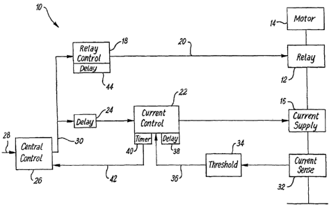
Fig. 1 shows a control arrangement 10 operable to control an electrical
relay 12 to supply current, for instance drive current to a motor 14. The
arrangement 10 has a current supply 16 for supplying current to the relay 12
for connection to the motor 14. A control arrangement at 18 provides a relay
make signal and a relay break signal at 20 to control the state of the relay
12 to
respectively make and break a connection between the current supply 16 and
CA 02440772 2003-09-12
WO 02/078030 PCT/GB02/01390
4
the motor 14. Current control arrangements indicated generally at 22 operate
to enable or disable the current supply 16. A first delay circuit 24 operates
to
delay the current supply 16 being enabled until after the relay control
circuit 18
has provided a relay make signal to the relay 12, so that the relay 12 is able
to
connect the current supply 16 to the motor 14 before the current supply 16
commences to supply current.
The inventor has appreciated that the introduction of this delay reduces
or eliminates the problem of arcing at the terminals of the relay 12, thus
increasing the expected life of the relay.
By way of example only, and in order to better illustrate the operation
and benefits of the apparatus being described, reference will be made to the
arrangement 10 being used to control a motor 14 which drives a sliding door.
However, the skilled reader will appreciate that similar principles can be
used in
other applications.
In more detail, the arrangement 10 has a central control circuit 26 which
receives instructions at 28, for instance from operator controls instructing
the
arrangement 10 to open or close the door operated by the motor 14. When door
operation is required, the circuit 26 instructs the relay control circuit 18
to
close the relay 12, thus connecting the motor 14 to the current supply 16. At
this stage, the current supply 16 has not yet commenced supplying current.
Thus, arcing at the contacts of the relay 12 is prevented.
In the example being described, the motor 14 is required to open or close
a door, as appropriate. This is achieved by the relay 12 being able to supply
motor current in either sense, as will be described more fully in relation to
Fig. 2.
The signal from the central control 26 to the relay control 18, at 30 is
also provided to the delay circuit 24. Thus, the signal 30 is common to the
relay control 18 and the delay circuit 24. After appropriate delay, the delay
CA 02440772 2003-09-12
WO 02/078030 PCT/GB02/01390
circuit 24 passes the common signal 30 to the current control circuit 22 which
then causes the current supply 16 to commence supplying current to the motor
14 through the relay 12. The delay introduced by the delay circuit 24 is set
to
allow the relay 12 sufficient time to close the relay contacts before the
current
supply 16 commences, thus preventing arcing at the relay contact, as noted
above.
The arrangement 10 also includes a current sensing arrangement at 32,
which senses the magnitude of current being supplied to the motor 14. A
threshold detector arrangement 34 detects if the current sensed at 32 has
exceeded a predetermined threshold. If so, the current control 22 is
instructed
at 36 to disable the current supply 16. A delay circuit 38, associated with
the
current control 22, then introduces a delay before the current control 22 is
again able to turn on the current supply 16. In the event that the cause of
the
excessive current has now passed away, continuous current supply will then
resume. However, in the event that the cause remains, the current will again
be
sensed as excessive, and current supply will again be disabled. Thus, the
arrangement of the current sensor 32, the threshold detector 34, the current
control 22 and the delay 38 serve to cause the current supply 16 to provide a
form of pulse width modulated (PWM) current supply which limits the power
delivered to the motor 14, thus protecting the motor 14 in the event that
abnormal operation has given rise to excessive current demands.
Examples of abnormalities which may give rise to excessive current
demands include a fault within the motor, or an inappropriate form of
operation, such as an instruction to open the door while a mechanical security
bolt is still engaged.
A timer circuit 40 monitors this PWM operation. If PWM operation
continues for a period in excess of a predetermined time, the timer 40 signals
this at 42 to the central control 26. In response, the central control 26
issues a
common signal 30 which disables current supply and breaks the relay. Further
delay 44 built into the relay control 18 causes the opening of the relay 12 to
be
CA 02440772 2003-09-12
WO 02/078030 PCT/GB02/01390
6
delayed beyond the discontinuing of current supply, again to prevent arcing at
the relay terminals.
The arrangement described above in relation to Fig. 1 is illustrated in
more detail in Fig. 2.
It is first appropriate to describe the relay arrangement 12. This has two
sets of contacts RL1, RL2 having their common contacts connected to respective
sides of the motor 14, which is a DC motor in this example, and their switch
contacts connected so that when the coils 48 of the relay 12 are de-energised,
the two sides of the motor 14 are connected together at 46, thus locking the
motor 14. Each set of contacts RL1, RL2 has an associated coil 48. When the
motor 14 is to run, one or other coil 48 is energised, as will be described,
to
connect the corresponding side of the motor to a positive supply at 50. Either
side of the motor 14 can be connected to one side of the power supply at 50,
by
energising the appropriate coil 48. The other side of the motor remains
connected through the other set of contacts RL1, RL2 to the common point 46,
which is in turn connected to the current supply 16, in the form of the
channel
of a MOSFET transistor 52 connected to the other side of the power supply at
54
through a series resistor 56.
.Consequently, DC current provided between the supply rails 50, 54 can
flow in either direction through the motor 14, according to the choice of coil
48
which is energised, thus allowing the motor 14 to be operated in either
direction, but subject to the control imposed by the transistor 52, which
supplies current to the motor only when turned on. Control arrangements for
the transistor 52 will be described below.
The control of the coils 48 occurs within the circuit 18, in response to
OPEN or CLOSE signals provided at 58 by a microcontroller 60 within the
central control 26. The voltage level of signals at 58A, 58B is low except
when
motor operation is required. When the OPEN signal S 8A is low, transistor 70
is
held off through resistor 72, thus preventing current through the coil 48
CA 02440772 2003-09-12
WO 02/078030 PCT/GB02/01390
7
controlling. terminals RL1. This leaves RLl in the position shown in Fig. 2.
When the motor 14 is required to open the door, the signal at 58A goes
high. The diode 74, which shunts resistor 72, is then forward-biased to turn
on
transistor 70 and thus conduct energising current through the coil 48 for
terminals RLl. Terminals RL1 thus switch, connecting the motor 14 in the
appropriate sense for opening the door (but subject to the control of the
transistor 52 as noted above).
It is important to note that there is substantially no time delay in
switching the relay terminals RL1 in response to signal 58A going high.
When door opening is no longer required, the microcontroller 60 returns
signal 58A to the low state. The gate of the transistor 70 does not
immediately
change state, being held high by capacitor 76 until the capacitor 76 has
discharged through resistor 72, with a time constant set by the values of the
resistor 72 and capacitor 76. This time constant introduces a delay between
the
signal 54A going low, and the transistor 70 switching, so that the current to
the
coil 48 for terminals RLl will not switch off until this delay has elapsed.
The
significance of this delay will be appreciated from the description set out
below.
It can readily be appreciated from Fig. 2 that control of the coil for
terminals RL2 is achieved by an equivalent circuit driven by the CLOSE signal
58B and for which same reference numerals are repeated, with the suffix A.
Control arrangements relating to the transistor 52 can now be described,
as follows.
The OPEN and CLOSE signals 58A, 58B are both applied to the base of
transistor 80, which is a bipolar transistor having a series collector
resistor 82,
the collector being directly connected to the gate of an FET transistor 84.
When
the motor 14 is not operating, both signals 58A, 58B are low, transistor 80 is
off, the collector of transistor 80 will be high, and transistor 84 will thus
be on.
CA 02440772 2003-09-12
WO 02/078030 PCT/GB02/01390
8
The channel of the transistor 84 is in series with a resistor 86 and
shunted by a capacitor 88, so that when the transistor 84 is on, the capacitor
'88
will be discharged, effectively having both terminals at the potential of the
ground rail 90.
When either the OPEN or CLOSE signal 58A, 58B goes high, transistor 80
will be switched on and its collector will go low, switching off transistor
84.
Capacitor 88 is then able to charge through resistor 86 so that the voltage at
the
point common to the transistor 84, resistor 86 and capacitor 88 will rise at a
rate determined by the time constant set by the values of the resistor 86 and
capacitor 88. This thus introduces a delay in the voltage rise at the common
point 92, as compared with the change at 58A, 58B.
The common point 92 is also the input to an inverter 94 whose output
controls the switch state of a transistor 96. The state of the inverter 94
thus
changes as the voltage at the common point 92 changes, but the change of state
of the inverter 94 is delayed by the delay described in relation to the
resistor 86
and capacitor 88. Switching of the transistor 96 is thus similarly delayed.
With
the signals 58A, 58B both low, the output of inverter 94 will be high and
transistor 96 will be switched on. When either signal 58A, 58B goes high, the
output of the inverter 94 will go low, after a delay, switching the transistor
96
off.
The switch state of the transistor 96 is used to override a circuit based
around transistor 98 and which controls the gate of the current transistor 52.
The collector of transistor 98 is connected to a positive supply rail 99 and
the
base is connected to the same positive supply rail, through resistor 100. The
base of transistor 98 is also connected to the collector of transistor 96.
Thus,
when transistor 96 is off, transistor 98 will be held on, thus holding the
gate of
transistor 52 at the positive supply rail potential and holding the transistor
52
turned on.
However, this tendency of transistor 98 to bias transistor 52 to turn on is
CA 02440772 2003-09-12
WO 02/078030 PCT/GB02/01390
9
overridden in the event that transistor 96 is on, as will be the position if
signals
58A, 58B are both low. In that event, the base of transistor 98 is held at
ground
rail potential through the transistor 96, which will be on. Transistor 98 is
thus
switched off and the gate of transistor 52 is similarly held at ground
potential,
switching off transistor 52. This will be the condition with signals 58A, 58B
both low. As a result, transistor 52 is switched off and current supply to the
relay 12 (and motor 14) is thus disabled.
However, in the event that either signal 58A or 58B goes high, the output
of inverter 94 will go low, after the delay described above, thus switching
off
transistor 96. This ceases to override the bias provided by transistor 98,
allowing transistor 52 to be turned on to begin supplying current to the relay
12. It is important to note that, as has been described above, turning on the
transistor 52 is delayed in response to the change of state of the signals 58A
or
58B, whereas switching of the relay terminals RL1, RL2 is not delayed. Thus,
the appropriate terminal RL1, RL2 will have switched before the transistor 52
turns on to supply current. This prevents arching in the terminals RL1, RL2 as
they switch.
When signals 58A, 58B again go low to switch off the motor 14, transistor
80 immediately switches off and transistor 84 immediately switches on.
Capacitor 88 immediately discharges through transistor 84. The input to
inverter 94 immediately goes low and the output of inventor 94 immediately
goes high. Transistor 96 immediately switches on, the action of transistor 98
is
immediately overridden and transistor 52 immediately switches off to disable
current supply to the relay 12. However, as described above, current to the
relay coils 48 is not cut off immediately, by virtue of the action of
capacitors
76A, 76B. The terminals RL1, RL2 do not immediately switch. The time
constants within the relay control circuit 18 are set to ensure that the
transistor
52 will have shut off current to the relay 12 before the terminals RL1, RL2
switch, thus again protecting the relay against arcing.
Additional protection within the system is provided by other
CA 02440772 2003-09-12
WO 02/078030 PCT/GB02/01390
components, which can now be described.
Resistor 56 has been described in series with the channel of transistor
52. Resistor 56 is used for current sensing. Current through resistor 56 gives
rise to a voltage across the resistor 56. This is sensed by a voltage divider
102
formed by two resistors 102A, 102B in series with each other and shunting
resistor 56. The common terminal of the resistors 102A, 102B thus has a
voltage level which rises or lowers in response to changes in current through
the current sensing resistor 56. This voltage level is thus a measure of
supply
current to the motor 14. The common terminal of the resistors 102A, 102B is
connected to the base of transistor 104 which acts as a threshold detector to
switch on when the voltage from the voltage divider 102 rises above the
switching voltage of the transistor 104. The collector of transistor 104 is
connected to the positive supply 99 through series resistor 106 and also to an
input of inverter 108. Consequently, when transistor 104 is turned on by
excessive motor current, the input to inverter 108 goes low and the inverter
output goes high. The inverter output is applied to the base of transistor 96
so
that in the event of excessive current being sensed, inverter 108 forces
transistor 96 to turn on, disabling current supply to the motor by switching
off
the transistor 52, as described above.
However, this state only remains for a period set by the delay circuit 38,
as follows. A further inverter 110 receives the output of the inverter 108 and
applies this to a resistor-capacitor time constant circuit 112. Thus, when the
output of inverter 108 has gone high, causing the output of inverter 110 to go
low, the RC circuit 112 retains the second input to inverter 108 low, until
the
RC circuit 112 has discharged. At this point, the inverter 108 is caused to
switch low, switching off transistor 96 and allowing transistor 52 to turn on
again, to recommence current supply to the motor 14. In the event that the
problem causing the excessive motor current has now gone away, normal
operation will resume. However, if the problem remains, excessive motor
current will again be sensed as described above, the transistor 52 will again
be
switched off for a period set by the RC circuit 112, and the transistor 52
will
CA 02440772 2003-09-12
WO 02/078030 PCT/GB02/01390
11
thus enter a form of pulse width modulation operation which limits the power
being provided.
While a short period of this pulse width modulation operation may be
acceptable, an extended period would indicate a significant problem existing.
Consequently, timer circuit 40 is used to monitor PWM operation and
completely shut down the arrangement in the event that PWM operation
continues for a period in excess of a predetermined time. This timing arises
as
follows. The output of the inverter 110 is applied to a further RC circuit
114,
the common terminal of which forms the input of a further inverter 116, the
output of which is provided to the microcontroller 60. During normal
operation, the output of inverter 110 will normally be high and the capacitor
of
RC circuit 114 will be discharged, holding the input of inverter 116 high and
providing a normally low signal at 118 to the microcontroller 60. However,
each time the output of inverter 110 goes low (as a cycle of the PWM operation
is executed), the capacitor of RC circuit 114 will receive additional charge,
so
that the input to inverter 116 will steadily reduce as PWM operation
continues,
until the inverter 116 changes state. This sends the overload signal 118 high,
indicating to the microcontroller 60 that PWM operation has continued for a
period in excess of the predetermined time (governed by the time constant of
the circuit 114), and in response, the microcontroller 60 will take both
signals
58A, 58B low, to disable the arrangement.
There is thus provided an arrangement in which arcing of the delay
terminals is prevented by ensuring that motor current is not flowing at the
time
the relay switches. In addition, excessive motor current is sensed, and
controlled by PWM modulation. In the event that excessive current continues,
the system is disabled.
It will be apparent that many variations and modifications can be made
to the apparatus described above, without departing from the scope of the
present invention. In particular, many details of the circuits shown in Fig. 2
and described above can be modified according to the particular intended
CA 02440772 2003-09-12
WO 02/078030 PCT/GB02/01390
12
application. Some of the functions provided by hardware in the arrangement
described above could alternatively be provided by software, for instance
within
the microcontroller 60. Thus, the microcontroller could provide the delay
function of the circuit 24, issuing appropriately timed circuits to make or
break
the relay and to turn the current transistor 52 on or off. Control of the PWM
operation, current sensing and the timing function of the circuit 40 could be
implemented wholly or partly by software. Component values and component
technology choices, including the choice of implementation in hardware or
software, will be within the knowledge of the skilled reader, as will
appropriate
alternatives. These are encompassed within the scope of the present invention.
Whilst endeavouring in the foregoing specification to draw attention to
those features of the invention believed to be of particular importance it
should
be understood that the Applicant claims protection in respect of any
patentable
feature or combination of features hereinbefore referred to and/or shown in
the
drawings whether or not particular emphasis has been placed thereon.