Note: Descriptions are shown in the official language in which they were submitted.
CA 02441054 2003-09-15
WO 02/073559 PCT/US02/07512
1
TRACKING DEVICE
CROSS-REFERENCE TO RELATED APPLICATIONS
This application claims the benefit of U.S. Provisional Application No.
60/275,519,
S filed on March 14, 2001, which is hereby incorporated in its entirety by
reference.
BACKGROUND
1. Field of the Invention
The present invention relates generally to tracking and locating objects and
people. More specifically, the invention relates to a device and method for
monitoring, tracking and locating an object or person, such as a child.
2. General Background and Related Art
Sometimes, when subjected to some adult activities such as shopping, a child
may become curious or restless. The child may have a tendency to wander. In a
matter of seconds, while the parent or guardian is distracted, a child can
move
quickly out of sight and become lost. In most instances, the child is nearby
but
merely out of sight, however, in other cases, the child may be placed into
danger.
To this end, monitoring and locating devices are used to quickly locate lost
children. Some types of monitoring and locating devices, usually the wireless
applications of the devices, include a transmitter which is positioned on the
child
such as, for example, around their wrist or ankle. The transmitter transmits
location
signals. Typically, a parent or guardian uses a receiver to receive the
transmitted
location signals from the child's transmitter to locate the transmitted
signal, which in
turn, leads them to their lost child.
In some cases, a number of such wireless devices may be used within close
proximity of other similar devices, such as, for example, in a shopping mall
or an
amusement park. In these cases, interference among the devices may be
possible,
which would render the devices inoperable and useless in locating lost
children.
CA 02441054 2003-09-15
WO 02/073559 PCT/US02/07512
2
Consequently, there exists a need in the art to provide a monitoring and
locating device capable of monitoring and locating an object or person, as
well as
being able to operate in close proximity to other monitoring and locating
devices.
The inventions claimed and / or described herein provide a tracking device
S which comprises one or more portable remote units (child units) and a
control unit
(parent unit) in radio frequency communication with each of the child units.
The
control unit is adapted to assign and transmit an individual identifier to
each portable
remote unit. The parent unit is constructed and arranged to continuously
monitor
each of the child units by transmitting and receiving signals to each of the
child units
using the individual identifiers assigned thereto.
The parent unit can be used with a single child unit or multiple child units,
each having a unique identifier. A plurality of operating channels can be used
and
methods are explained for selecting an operating channel for a particular
parent
child unit pair. These methods generally include a scheme for stepping
incrementally through one or more available channels of a particular frequency
band, with each of the plurality of channels having a numbered sequence. A
plurality of channels can be stepped through in sequential order from a lowest
numbered channel of the sequence to a highest numbered channel of the
sequence.
Or other channel stepping techniques can be used. Stepping through channels
can
be repeated as needed. Another possible approach includes hopping randomly
through the sequence of channels based at least in part on a predetermined
algorithm. Such algorithm might be, for example, to selected a channel from
the a t
low, mid or high portion of a frequency band.
Other aspects, features and advantages of the inventions claimed and / or
described herein will become apparent from the following detailed description,
the
accompanying drawings, and the appended claims.
BRIEF DESCRIPTION OF THE DRAWINGS
Figure 1 is a block diagram of a monitoring and locating system 40
according to the inventions;
Figure 2 is a block diagram of the parent unit 42 shown in Figure 1;
CA 02441054 2003-09-15
WO 02/073559 PCT/US02/07512
3
Figure 3 is a block diagram of a child unit 44 shown in Figure 1;
Figure 4 is an illustration of electrical circuitry implemented in the parent
unit according to an exemplary embodiment;
Figure 5 is a detailed block diagram of the direction detector 530 shown as a
single block in Figure 2;
Figure 6 is illustrates the logical structure of the power control circuitry
of
the parent unit;
Figure 7 is illustrates the logical structure of the range selection circuitry
of
parent unit 42;
Figure 8 explains how direction is displayed;
Figure 9 is an illustration showing the logical structure of the keybutton
circuit according to an exemplary embodiment;
Figure 10 is a schematic diagram showing an exemplary embodiment of
sound generator 538 of parent unit 42 shown in Figure 2;
Figure 11 is a schematic diagram showing an exemplary embodiment of
sound generator 722 of child unit 44 shown in Figure 3;
Figure 12 is a schematic diagram of an exemplary embodiment of circuitry
54 of a child unit 44;
Figure 13 is a schematic diagram of the control section of a child unit 44;
Figure 14 is a schematic diagram of the RF and data filter section of a child
unit 44;
Figure 15 is a schematic diagram of an exemplary logical structure of the
power control circuitry of a child unit 44;
Figure 16 is a schematic diagram of an exemplary logical structure of the
proximity detection circuit;
Figure 17 is a schematic diagram of an exemplary logical structure of a water
detection circuit;
Figure 18 is chart illustrating the relationship of symbols to bits and the
Manchester code according to an exemplary embodiment;
Figure 19 is chart illustrating the tracking transmission of the child units
according to an exemplary embodiment;
CA 02441054 2003-09-15
WO 02/073559 PCT/US02/07512
4
Figure 20 is a chart illustrating the direction finding mode timing of the
parent unit implemented according to an exemplary embodiment, the direction
finding mode is being used with antenna switching for phase detection;
Figure 21 is a flow chart of an exemplary method for selecting an operation
channel;
Figure 22 is a flow chart of an exemplary method of operation;
Figure 23 is a flow chart illustrating operations performed during powering
on of parent unit 42;
Figures 24 and 25 are flow charts illustrating operations performed during
power down of parent unit 42, figure 24 showing detail of step 110;
Figures 26 and 27 are flow charts illustrating operations performed during a
status check of the parent unit, figure 26 showing detail of step 130 and
figure 27
showing detail of step 1 S0;
Figure 28 is a flow chart illustrating operations performed during polling in
accordance with the exemplary embodiment of the invention for a first child
unit 44;
Figure 29 is a flow chart illustrating operations performed during polling in
accordance with the exemplary embodiment of the invention for a second child
unit
44;
Figure 30 is a flow chart illustrating operations performed during polling in
accordance with the exemplary embodiment of the invention for a third child
unit
44;
Figure 31 is a flow chart illustrating operations performed during poll
response checking in accordance with the exemplary embodiment of the
invention;
Figures 32 and 33 are flow charts illustrating operations performed during
tracking in accordance with the exemplary embodiment of the invention;
Figure 34 is a flow chart illustrating operations performed during direction
display in accordance with the exemplary embodiment of the invention;
Figure 35 is a flow chart illustrating operations performed during
initialization of the child unit;
Figure 36 is a flow chart illustrating further operations performed from
Figure 33 by the child unit when interpreting commands from the parent unit;
CA 02441054 2003-09-15
WO 02/073559 PCT/US02/07512
Figure 37 is a flow chart illustrating further operations performed from
Figure 36 by the child unit when interpreting commands from the parent unit;
Figure 38 is a flow chart illustrating further operations performed during
checking the status condition of the child unit from Figure 35;
5 Figure 39 is a flow chart detailing step 329 shown in Figure 36;
Figure 40 is a flow chart detailing step 321 shown in Figure 36.
DETAILED DESCRIPTION
Figure 1 is a block diagram showing the schematic arrangement of a
monitoring and locating device constructed according to the inventions. The
monitoring and locating device, generally indicated by reference numeral 40
includes a master control (hereafter referred to as parent unit), generally
indicated by
reference numeral 42, and one or more portable remote units (hereafter
referred to as
child units), generally indicated by reference numeral 44, in communication,
e.g.,
radio frequency (RF), with the parent unit 42. The parent unit 42 acquires
each of
the plurality of child units 44 by assigning the child units 44 an individual
identifier
or ID code, generally indicated by 46. The parent unit 42 monitors and tracks
each
child unit 44 by transmitting and receiving signals including the ID code 46
to and
from the child units 44, such that the parent unit 44 may be used to locate a
selected
child unit from the one or more child units 44. For example, the ID codes 46
may
include a modulated RF signal carried by a RF carrier signal.
The parent unit 42 and each child unit 44 may include an enclosure or
housing 48, 52, respectively. Each housing 48, 52 may be designed to protect
electrical circuitry S0, 54, respectively, and may be configured to allow the
parent
unit 42 to communicate (i.e., monitor, track and locate) with the child units
44. For
example, the housings 48, 52 may be any configuration and either made of
plastic or
any other material capable of protecting electrical circuitry or electrical
components.
The housings 48, 52 may have a fastener structure, such as a clip, a fanny
pack (i.e.,
a waistband), or some other fastener means, configured to releasably attach to
an
object, such as, for example, an adult, a parent, a child, a pet or some other
living
CA 02441054 2003-09-15
WO 02/073559 PCT/US02/07512
6
entity. For example, the clip may attach to a belt or other garment of the
person's
clothing or the fanny pack may be releasably attached around a person's waist.
The housings 48, 52 may have portions which are configured to receive a
keypad, i.e., numeric or alphabetic, key buttons, power buttons or any other
user
interface structure which may be operatively connected with the respective
electrical
circuitry S0, 54.
Parent unit 42 and the child units 44 communicate with one another using a
variety of predetermined commands or messages, which may be transmitted to and
from the parent and child units 42, 44, respectively, using the ID codes 46.
For
example, normal poll may represent the parent unit 42 transmitting a signal to
and
receiving a signal from each of the child units 44. Poll acknowledge may
represent
the child unit 44 transmitting a signal to the parent unit 42. Similarly, poll
acknowledge with a low battery may represent the child unit 44 transmitting a
signal
to the parent unit 42, but having a low battery. It is contemplated that other
commands, such as, poll acknowledge with channel change, which may represent
the child unit 44 transmitting a signal to the parent unit 42 and requesting
to change
the operating channel, may be used as well.
Change channel may represent the parent unit 42 communicating to the child
units 44 that the operating channel is being changed. ID assignment may
represent
the parent unit 42 assigning the ID code 46 to each of the child units 44.
Search
command may represent if the parent unit 42 is searching for or attempting to
track
one of the child units 44. Search response may represent the child units 44
responding to the search command initiated by the parent unit 42. Panic may
represent the help button (i.e., S9) of one of the child units 44 being
activated.
Power off may represent the parent unit 42 initiating powering off the
circuitry 54
via software and the circuitry 50. Request ID and confirm ID acquisition may
represent the child units 44 requesting the ID codes 46 from the parent unit
42 and
the child units 44 responding to the parent unit 42 that the ID code 46
assigned
thereto has been confirmed.
Figure 2 is a block diagram of the parent unit 42 shown in Figure 1. Signals
from a 'child' unit are received by a pair of antennas 502 and 504. An antenna
CA 02441054 2003-09-15
WO 02/073559 PCT/US02/07512
7
switch 506 switches based on a control signal 508 from a microprocessor unit
510.
The microprocessor unit is advantageously selected to be a PIC 16L73B made by
Microchip Technology, Inc. This is the presently preferred selection.
Alternatives
can be used with the appropriate design changes. Switching is controlled so
that
antennas 502 and 504 are alternately connected to a signal line 512 of antenna
switch 506. Signal line 512 is coupled to a transceiver system 514 including a
transceiver 516 so that the transceiver system can transmit signals to and
receive
signals from antennas 502 and 504 via antenna switch 506. Transceiver 516 is
advantageously selected to be an RF2945 made by RF Micro Devices, Inc. This
particular device merely represents the presently preferred choice.
Alternatives can
be used. For example, a transceiver with a built in synthesizer could be used.
Such
an arrangement would eliminate the need for a separate synthesizer.
A frequency synthesizer 520 provides required signals to transceiver system
514 via a signal line 522. The presently preferred choice for frequency
synthesizer
is an LMX2316 made by National Semiconductor. Alternatives can be used.
Frequency synthesizer 520 is controlled by microprocessor unit 510 via a line
554.
Transceiver system 514 and microprocessor unit 510 are connected via a signal
line
524 so that the microprocessor unit 510 can control the operation of
transceiver
system 514. A data filter 560 is interposed between transceiver system 514 and
microprocessor unit 510 via lines 562 and 564. Information output from
transceiver
system 514 is coupled to a direction detector 530 via a signal line 532.
Direction
detector 530 provides its output information to microprocessor unit 510 via a
signal
line 534. Microprocessor unit 510 processes information received from
direction
detector 530 and drives various controls and indicators 536 and a sound
generator
538 via respective signal lines 540 and 542 to provide a human interface with
the
user. Microprocessor unit 510 also controls a power control circuit 544 via a
signal
line 546. Power control circuit 544 provides power and control to active
circuits of
the monitoring and locating device via a line 548. A power supply 550 provides
power to power control circuit via line 552. As used herein 'line' can refer
to
multiple line cables, where appropriate.
CA 02441054 2003-09-15
WO 02/073559 PCT/US02/07512
8
For the purpose of this description, it is assumed that the child unit is at
some
distance from the parent unit and that the system has been placed in the
"direction
finding" mode. Antennas 502 and 504 (see Figure 2) are mounted within (or on)
the
parent unit 42. For direction finding purposes, parent unit 42 is held, in the
hand of
the operator, such that each of antennas 502 and 504 is approximately equal
distance
from the operator's face. As he holds and maintains parent unit 42 in this
position
and rotates his body, the physical distance of each of antennas 502 and 504
will
change relative to that of the child unit. Direction is determined by
measuring the
electrical phase angles of respective antenna signals. Antennas 502 and 504
are
physically mounted within or on parent unit 42 such that they are spaced apart
by
not more than one-quarter wavelength, or 90 electrical degrees at frequencies
being
used . Thus the relative electrical phase angle, measured at the antenna
terminals,
can never be greater than plus or minus 90 degrees, regardless of antenna
orientation. When the antennas are equal distance from the child unit 44, the
measured phase angle difference between antennas 502 and 504 will be 0
degrees,
because a signal from child unit 44 arrives at both antennas at the same time.
As
parent unit 42 is physically rotated, one antenna becomes slightly closer to
child unit
44 as compared to the other. This will cause a phase difference between the
signals
from antennas 502 and 504. The antenna that is closer to the child unit 44
will
"lead" in phase because the signal arrives at this antenna earlier. Thus, if
parent unit
42 rotates 360 degrees, the electrical phase angle difference will change by
plus or
minus 90 degrees (twice for each rotation).
The signals from antennas 502 and 504 are amplified before useful
information is extracted. If two phase coherent receivers (one for each
antenna) are
connected to the antenna terminals, then the amplified signal from each
receiver can
be input to a phase detector and the resultant voltage from the detector can
be
processed to obtain the direction of child unit 44.
However, it is more desirable to use only one receiver from the standpoint of
minimizing cost and complexity. In order to use a single receiver, the two
antennas
must be multiplexed. This is accomplished by the use of antenna switch 506.
Antenna switch 506 is essentially a single pole, two positions, RF switch.
Switching
CA 02441054 2003-09-15
WO 02/073559 PCT/US02/07512
9
between antennas is accomplished by applying a control signal to antenna
switch
506 via signal line 508. When the control signal is in one state, the left
antenna 502
is selected, and when the control signal switches to the opposite state, the
right
antenna 504 is selected. Thus, signals from antennas 502 and 504 can be
alternately
coupled to transceiver 516 in a time-multiplexed manner. Because the signals
from
antennas 502 and 504 are never present simultaneously, phase information from
each of the antennas is temporarily stored and the stored phases are compared.
One way to accomplish this is to temporarily store the phase information
from one of the antennas 502 and 504 and then immediately compare it with the
phase information from the other of the antennas. In this case the phase
detector
output is a pulse whose amplitude is a function of the phase angle between the
signals from antennas 502 and 504 and whose duration is equal to the antenna-
switching rate.
An alternative would be to store the information from one of the antennas
and then to store the information from the other of the antennas. Then compare
the
two stored pieces of information. Actual phase comparison is carried out in
direction
detector 530. In this configuration the phase detector's output has a non-
pulsed
amplitude that is a function of the phase angle between the signals from
antennas
502 and 504. The antenna-switching rate is selected so that it is appropriate
for the
frequencies used and phase comparisons to be made. If switching (sampling) is
carried out at too slow a rate, each antenna spends more time in a given state
and
there is a higher probability that the information stored will not be valid.
This is true
because the antenna phase "in a real world situation" is constantly changing.
For
example, the child is running and the parent is moving, therefore, the
antennas are
constantly changing phase. It has been determined that the antenna-sampling
rate
should be in the range of 1/4 to 1/6 of the carrier frequency. This becomes
impractical if the carrier frequency is high in comparison to the bandwidth of
the
system. To overcome this problem the carrier is mixed down to a much lower
frequency.
"Mixing down" preserves the phase information and at the same time allows
a lower sampling rate. The IF frequency of transceiver 516 is advantageously
CA 02441054 2003-09-15
WO 02/073559 PCT/US02/07512
selected to be 10.7 MHz. This is still to high to get a practical sampling
rate for the
information bandwidth. In this system the 10.7 MHz is mixed again to
approximately 300KHz. This allows the sampling rate to be set to 50 to 75KHz,
which is practical for this system. Other frequencies can be used. The
frequency
5 specified is presently considered to be the best mode for carrying out the
inventions
defined herein.
Processing the sampled phase information to obtain the direction information
can be accomplished in a number of ways. The presently preferred way is to use
a
software algorithm and a DSP (Digital Signal Processor). An alternative would
be
10 to use a microprocessor with sufficient processing power. The presently
preferred
approach is considered to be the most practical at the time this document was
prepared. Other approaches may be more practical in the future.
Figure 3 is a block diagram of a child unit 44 shown in Figure 1. Signals
transmitted from the parent unit are received by antenna 702 which feeds the
signal
line 704, a microstrip transmission line. Signal line 704 is coupled to a
transceiver
system 706 including a transceiver 708 so that the transceiver system can
either
transmit signals to, or receive signals from, antenna 702. Transceiver 706 is
advantageously selected to be an RF2945 made by RF Micro Devices, Inc. This
particular device merely represents the presently preferred choice.
Alternatives can be used with appropriate design changes where necessary.
A frequency synthesizer 710 provides required signals to transceiver system
706 via
a signal line 712. The presently preferred choice for frequency synthesizer is
an
LMX2316 made by National Semiconductor. Alternatives can be used, for
instance, Transceivers are available with built in Synthesizers, eliminating
the need
for a separate synthesizer. Frequency synthesizer, 710 is controlled by
microprocessor unit 720, via a line 718. Transceiver system 706 and
microprocessor
unit 720, are connected via a signal line 716 so that the microprocessor unit
720 can
control the operation of transceiver system 706.
A data filter 714 is interposed between transceiver system 706 and
microprocessor unit 720 via lines 734 and 736. Microprocessor unit 720
processes
information received from the parent unit via the transceiver system 706 and
in turn,
CA 02441054 2003-09-15
WO 02/073559 PCT/US02/07512
11
sends this information to the data filter 714 to remove noise from the
received data.
The microprocessor then performs further processing and transmits back a
response
to the parent unit. Upon certain commands received from the parent unit, the
microprocessor unit drives a sound generator 722 via respective signal lines
738, to
provide audible aid in the parent finding the child.
Microprocessor unit 720 also controls a power control circuit 726 via a
signal line 730. Power control circuit 726 provides power and control to the
active
circuits via line 732. A power supply 728 provides power to the power control
circuit via line 740. Additionally the power control unit monitors and sends
battery
charge status to the microprocessor. The microprocessor 720, in turn sends a
"low
battery" coded message via data via line 716, to the transceiver systems. The
transceiver system transmits the warning message, to the parent unit. As used
herein
'line' can refer to multiple line cables, where appropriate.
Figure 4 is a schematic diagram showing some of the electrical circuitry 50
of parent unit 42. Some of the 'blocks' correspond to functional blocks shown
in
Figure 2. RF signals are transmitted or received through transceiver system
514. In
the receive mode, a signal output from transceiver system S 14 is filtered
through the
data filter 560 then passed on to the microprocessor unit 510, where the data
is
processed. When in the tracking mode, the direction detector 530 feeds data to
microprocessor unit 510. Microprocessor unit 510 processes the data and drives
controls and indicators 536 (see Figure 2).
Figure 5 is a more detailed block diagram of direction detector 530. Signal
line 532 from an IF stage of transceiver 516 is coupled to an input of an
amplifier/buffer 602. An output of amplifier/buffer 602 is coupled to an input
of a
mixer and IF filter 604 which also receives a signal from a crystal controlled
local
oscillator 606. An output from mixer and IF filter 604 is coupled to an input
of a
comparator 608.
An output of comparator 608 is coupled to a pair of synchronous switches
612 and 614, controlled by respective I and Q control signals from
microprocessor
unit 510. Output from synchronous switch 612 is coupled to a band pass filter
I 616.
Output from synchronous switch 614 is coupled to a band pass filter Q 618.
Band
CA 02441054 2003-09-15
WO 02/073559 PCT/US02/07512
12
pass filters 616 and 618 are respectively tuned by analog signals from
respective
digital to analog converters 622 and 624 which are controlled by
microprocessor
unit 510.
Output of band pass filter 616 is coupled to a phase shifter 630 and detector
632. Output of band pass filter 618 is coupled to a comparator 640 and a
detector
642. Outputs of detectors 632 and 642 are coupled to microprocessor unit S 10.
Output of phase shifter 630 is coupled to comparator 650 Output from
comparator
650 is coupled to an "I" input of a phase detector 660. Output from comparator
640
is coupled to a "Q" input of phase detector 660. Output of phase detector 660
is
coupled to microprocessor unit 510.
Amplifier and buffer 602 buffers the signal obtained from the IF of
transceiver S 16. The buffer portion of amplifier and buffer 602 minimizes the
loading effect on transceiver 516. The output of amplifier and buffer 602 is
coupled
to mixer and IF filter 604, which mixes the 10.7 MHz IF signal with an 11 MHz.
signal from Crystal Controlled Local Oscillator 606. The resultant IF signal
includes sum and difference components of the two signals. The difference
signal
(300KHz) is filtered at the output of mixer and IF filter 604 and coupled to
an input
of voltage comparator 608.
Comparator 608 provides a well defined 300KHz. square wave output. The
square wave signal from comparator 608 is coupled to two synchronous switches
612 and 614. Switches 612 and 614 can be implemented by the use of logic gates
that operate as synchronous switches. The switches, operating in sync with the
antenna switch 506 (Figure 2), separate a serial signal from comparator 608
into left
and right antenna signals (called "I" and "Q"). These signals appear as
"bursts".
Each burst has a duration equivalent to the time that the antenna is connected
to the
receiver input. If, for example, the sampling rate is 50 KHz., one will
observe
repeated 3 cycle bursts at the output of each gate. It is not necessary that
the
sampling be harmonically coherent with the IF signal. It simply means that the
bursts will not be exactly 3 cycles. The "I" signal is fed into a narrow band
bandpass filter 616. The "Q" signal is fed into narrow band bandpass filter
618.
Filters 616 and 618 provide the storage of phase information obtained from the
two
CA 02441054 2003-09-15
WO 02/073559 PCT/US02/07512
13
antennas. This occurs in the following manner: The burst signal excites the
narrow
bandpass filter. When the burst ends the bandpass filter continues to "ring"
at the
burst frequency. The result is a continuous signal at the output of each
filter that
contains the phase information of the signals that were received at the
antennas.
Since the bandpass filters are narrow band, it is important that they maintain
resonance at the center of the 300KHz. frequency. The IF frequency may not
actually be 300KHz. because of drift in the local oscillators of the system.
To assure
that that the filters are tuned at the exact IF center frequency, filters 616
and 618 are
implemented as electronically tunable filters and microprocessor unit 510 is
programmed to periodically retune these electronically tunable filters. In
order to
tune filters 616 and 618, the signal amplitude of each filter's output is
"peaked."
To accomplish this peaking amplitude detectors 632 and 642 are provided at the
respective outputs of filters 616 and 618. Respective outputs of detectors 632
and
642 are input to analog input ports of microprocessor unit 510. Microprocessor
unit
510 outputs a digital signal to digital-to-analog converters 622 and 624.
Converters
622 and 624 output a tuning voltage to each filter.
As an alternative, it is possible to arrange for this function to be carried
out
another way. It is possible to eliminate the detectors and sample the signal
out of
the filter if the microprocessor is capable of processing these signals
directly.
Because of the narrow band characteristics of bandpass filters 616 and 618,
the harmonic components that make up the square wave have been removed,
therefore, a sine wave appears at their output. Phase detector 660 requires a
square
wave input. Therefore, the sine-wave signals need to be converted back to
square
waves. This is accomplished by feeding each sine-wave signals into its
respective
comparator 650 and 640. The outputs of comparators 650 and 640 are input to
the
phase detector 660.
Phase detector 660 requires that the input signal, range in phase from 0 to
180 degrees. It provides a corresponding output voltage of 0 to approxirmately
plus
3 volts. However, the antennas provide a phase shift of 0 degrees to plus or
minus
90 degrees. To resolve this incapability, the phase of one of the two signals
that are
input to the detector is shifted by 90 degrees. A 90-degree phase shift
circuit 630 is
CA 02441054 2003-09-15
WO 02/073559 PCT/US02/07512
14
inserted between filter 616 and its corresponding comparator 650. When parent
unit
42 is pointed directly toward child unit 44, phase detector 660 outputs a
voltage of
approximately 1.5-volts. When child unit 44 is to the left of center, the
detector will
output a voltage of less than 1.5-volts and when the child unit is to the
right of
center, the detector will output a voltage of greater than 1.5-volts.
Therefore, the
magnitude of the output voltage is a function of the phase shift at the
antennas.
The output of phase detector 660 is input to an analog port of the
microprocessor unit 510, where it is processed prior to driving the direction
indicators (see software flow diagram).
Microprocessor unit 510 may be any logical processor configured to process
logical instructions. In the illustrated embodiment, the microprocessor unit
510 is
programmed to generate the ID codes 46 for each child unit 44 and may be
configured to store the ID codes 46 therein.
The microprocessor unit 510 has a number of different operating modes,
some of which may include sleep mode, track mode, poll receive mode, track
receive mode, track mode, or direction detect mode.
A power supply 550 may supply power to the microprocessor unit 510. In
the illustrated embodiment, the power supply 550 is a DC voltage provided by
batteries that are rechargeable or disposable. Alternatively, 120 volt or 240
volt AC
to DC power adapter may be supplied to the unit. The parent unit 42 may be
adapted
to include circuitry for recharging the power supply 550. The parent unit 42
may
also include a battery strength indicator.
Figure 6 is a schematic diagram explaining power control in parent unit 42
(see functional block 544 in Figure 2). A range select switch 65 is coupled
with a
range select circuit so that the range select switch can control a range
select switch
state. This state is multiplexed onto the same pin as is the power button
state, thus
they are considered together. The range select switch 65 is implemented so
that a
user can select a number of different operating ranges for communication
between
the parent unit 42 and the child units 44.
A "power button" is constituted by two normally open switches, S6 and S7
ganged together. When the power button (S6 and S7) is pressed, switches S6 and
CA 02441054 2003-09-15
WO 02/073559 PCT/US02/07512
S7 are closed. When switch S6 is closed Vbatt is connected to the enable pin
of a
voltage regulator, 64 and a source voltage VCC of 3.0 volts is provided to the
microprocessor unit 510. The voltage regulator unit is advantageously selected
to be
a Micrel Semiconductor Inc., part number MIC5205-3Ø This is the presently
5 preferred selection. Alternatives can be used with the appropriate design
changes. In
order for the power supply (see 550 in Figure 2) to continue to provide power,
a
power on latch PWR ON LATCH* (i.e., port RCS of a microprocessor unit 510)
must be set low before the user has the opportunity to cease pressing the
power
button (S6 or S7).
10 Essentially VCC is applied in response to the user pressing the power
button
(S6 and S7). This, causes microprocessor unit 510 to turn on. In child unit
44,
when the child unit's power button (S8 or S9) is depressed, microprocessor 720
(see
Figure 3) asserts the power on latch PWR ON LATCH* (i.e., port RCS), which
randomly assigns the ID code 46 to child unit 44. Each ID code 46 is a 8-bit
15 number generated by microprocessor 510 that includes 6 bits randomly
assigned by
microprocessor unit 510 during power up and 2 bits representing a number of
one of
the child units 44 is then appended to the 6 bit randomly assigned number. In
general, multiple 8-bit numbers may be used to accommodate additional child
units
44. For example, the number of 8-bit numbers implemented within each
monitoring
and locating device 40 depends upon the number of child units 44 associated
and in
communication with and the parent unit 42.
To turn the parent unit 42 off in the illustrated embodiment, the power button
(S6 and S7) is pressed and held for a predetermined minimum amount of time,
for
example, 1 second. As a result, microprocessor 510 can read VCC on port ANO.
This voltage indicates the parent unit 42 is to be powered off with the power
on latch
PWR ON LATCH* (i.e., port RCS) being set high and the voltage regulator 64 is
shut down or disabled.
The range select function is shared with the power control circuitry on port
ANO. When the power switch (S6 and S7) is not depressed, the state of the
range
select switch is presented to the port ANO as one of three analog voltages.
These
CA 02441054 2003-09-15
WO 02/073559 PCT/US02/07512
16
analog voltages may be interpreted using an analog to digital converter (A/D
converter).
Examples of range switch parameters for a high switch state in the illustrated
embodiment may include a voltage of 0.94 volts with a minimum A/D value of 74
and a maximum A/D value of 86. For a middle switch state, an exemplary range
of
switch parameters may include a voltage of 1.5 volts with a minimum A/D value
of
122 and a maximum A/D value of 134. Exemplary range switch parameters for a
low switch state may include a voltage of 2.0 volts with a minimum A/D value
of
165 and a maximum A/D value of 177. With the power button S6 or S7 depressed,
the exemplary range of switch parameters may include a voltage of 2.7 volts to
3.3
volts with a minimum A/D value of 240 and a maximum A/D value of 255.
Essentially the user presses the power button (S6 or S7) for at least the
predetermined minimum amount of time to indicate a switch off. Microprocessor
unite 510 waits for the power button (S6 and S7) to be released then deasserts
or
releases the power on latch PWR ON LATCH* (i.e., port RCS), which allows the
energy source VCC to be turned off.
Figure 7 is a schematic diagram explaining the logical structure of the range
selection function of parent unit 42. Transceiver system 514 (see Figure 2) is
coupled to microprocessor S 10 . Transceiver system 514 (see Figure 2)
transmits
and receives its signals via separate antennae 502 and 504 configured to
transmit and
receive modulated RF signals to and from the child units 44. The antennae 502
and
504 may alternately transmit command signals and the ID codes 46 to each of
the
child units 44 and can also receive signals from the child units 44.
The antennae 502 and 504 may either transmit or receive, but the antennas
do not perform both simultaneously. Another antenna switch, within the
transceiver
system, operates in a half duplex mode, thus allowing the antennas 502 and 504
to
perform the function of transmission or reception. At the same time it
prevents the
transmission output power from damaging the transceiver, receiver input.
Transmission and reception can occur on the same frequency, but it is not
necessary
that they do so.
CA 02441054 2003-09-15
WO 02/073559 PCT/US02/07512
17
In the illustrated embodiment, a data filter, implemented as a low-pass filter
58 is provided to deliver an energy signal, such as a 3.0-volt Complementary
Metal
Oxide Semiconductor (CMOS) signal, to microprocessor unit 510. As illustrated,
the data filter, implemented as low-pass filter 58 is auto-referenced with
unity DC
gain and optimized for a lOK symbol per second received signal. The low-pass
filter 58 may be operatively connected with, e.g., followed by, a data-dicer,
however, any configuration is possible.
In the RF section (part of transceiver system 706) of the parent unit 42, RF
level control is provided by a pulse width modulator (PWM). The PWM signal
(i.e., PWM OUT) is transmitted from pin RC2, pin 13 of microprocessor unit 510
and is intended to drive two mutually exclusive circuits. When microprocessor
unit
510 is operating in the transmit mode, the PWM signal (i.e., PWM OUT) provides
the output voltage for adjusting the RF level of the RF. When microprocessor
unit
510 is in tracking mode, the PWM signal (i.e., PWM_OUT) is used to control the
switching between the antennae 502, 504.
In the illustrated embodiment, the PWM signal (i.e., PWM_OUT) is
multiplexed using a high speed switch 69, which is controlled by the TX EN
signal.
For example, when the TX EN signal is true (a logic one or a high voltage),
the
PWM signal (i.e., PWM OUT) may be routed to transceiver 708 which may be
implemented as a transceiver or RF chip, such as RF2945, via a low pass
filter. For
example, the PMW OUT signal is a digital signal that is pulse width modulated.
In
the transmit mode, the duty cycle is used to generate an analog value to
provide
proper RF power. In direction finding mode, the signal is used for switching
antenna at approximately 50 KHz. rate, as will be described below.
In the illustrated embodiment, when the TX EN signal is high, the PWM is
used to provide the transmit level power adjust output. It may be preferable
that the
PWM output port pin be programmed to a high impedance state during the poll
receive mode of microprocessor unit 510.
The transmit power level is determined by the analog signal received by
transceiver 708 at its LVL ADJ input. The LVL ADJ input accepts an analog
signal from a predetermined range of energy values, such as 0.0 volts to 3.0
volts.
CA 02441054 2003-09-15
WO 02/073559 PCT/US02/07512
18
For example, analog signals below 0.7 volts cause the transmit power to be set
to a
minimum energy value, i.e., 0.0 volts, while maximum transmit power may be
achieved, for example, an energy value equaling, for example, 3.0 volts DC.
The
analog signal to drive LVL ADJ may be generated by filtering the PWM signal
(i.e.,
PWM-OUT) with low-pass filter 58. In the illustrated embodiment, the parent
unit
42 transmits at the power specified by a range switch, such as range switch
65,
except for mode change commands. Alternatively, in the child units 44, the
transmit
power level may be set at the highest attainable level at all times.
In the illustrated embodiment, when the TX EN signal is false (a logic zero
or a low voltage), TX EN* goes high and then the PWM signal (i.e., PWM-OUT) is
routed to the RF LVL ADJ in transmit mode. Alternatively, when the TX EN
signal is low, the PWM signal may be gated on the ANT CNTL signal in order to
control the switching between the antennae 502, 504 in direction finding mode.
The antennae 502, 504 may be alternated between receive polls, wherein one
poll constitutes transmitting a signal to and receiving a signal from each of
the child
units 44. In normal mode of microprocessor unit 510, the antenna switching is
controlled by an antenna control switch having an ANT_SW CNTL signal that is
transmitted from port RC1, pin 12, of microprocessor unit 510 and is received
by
port YD, pin 10 of the high speed switch 69.
Although antennae 502, 504 may be alternated at any rate between SOKHz
and 75KHz it may be preferable to set the input antenna switch rate at
approximately
50 kHz when microprocessor unit 510 is in tracking mode.
Figure 8 explains how direction is displayed. Direction display is part of the
"controls and indicators" 536 shown in Figure 2. It is coupled to
microprocessor
unit 510 so that it can be driven to display the relative position of a
selected child
unit 44 relative to the parent unit 42 in response to information provided by
direction
detector 530. This occurs when the parent unit 42 is in the direction finding
mode.
In the illustrated embodiment, commands and responses from the child unit 44
to
enter the direction finding mode are sent using the ID codes 46.
The direction display 70 includes a number of direction LEDs 75, for
example a left LED, a right LED and a center LED. Of the three direction LEDs
75,
CA 02441054 2003-09-15
WO 02/073559 PCT/US02/07512
19
one or none may be commanded to light at any single time or at any frequency
by
microprocessor unit 510. The operation of the direction display 70 is
controlled by
the states of the RC3 and RBS ports of microprocessor unit 510. For example,
if the
RC3 port and the RBS port are both 0, then the direction LEDs are turned off.
If the
RC3 port is 0 and the RBS port is 1, then the left LED is turned on or lit. If
the RC3
port is l and the RBS port is 0, then the center LED is turned on or lit and
if the RC3
port and the RBS port are both 1, then the right LED is turned on or
illuminated.
In this exemplary embodiment, frequency synthesizer device 520 (see Figure
2) is coupled to microprocessor unit S 10 and to the transceiver system 514,
which
includes a transceiver or RF chip, such as RF2945, as described above. The
frequency synthesizer device 520 constitutes the operating channel selection
circuit
of the monitoring and locating device 40. The frequency synthesizer device 520
selects an operating channel on a frequency band for the parent unit 42 to
transmit
signals to and receive signals from the child unit 44 on the selected
operating
1 S channel. The selected operating channel may be used for transmission or
reception
and may be set by appropriately programming the frequency synthesizer device
520,
such as, for example, by clocking an array of signals in a control pattern
when
programming the frequency synthesizer device 520. It is preferable to program
the
frequency synthesizer device 520 while the transceiver system 514 is in VCO
mode
to prevent RF noise, however, the transceiver system 514 can be in any mode
thereof, such as a track mode thereof or a sleep mode thereof.
As shown in Figure 7, a range selection circuit that may include the range
selection switches 65. The microprocessor unit 510 may control a sound
generator
538 (see Figure 2), which may be used as an indicator for alarms or warnings,
such
as low battery detection, as will be described below. Sound generator 538
includes
one or more speakers for providing audible information such as warnings to the
user.
The speaker may be rendered inoperative when the RF signal is above a
minimum strength, i.e., is received by the parent unit 42, but activated when
the RF
signal falls below the minimum strength, i.e., is not received by the parent
unit 42.
The minimum strength to correspond to a certain predetermined distance between
the parent unit and the selected child unit, whereby the user might select
between
CA 02441054 2003-09-15
WO 02/073559 PCT/US02/07512
different predetermined distances via range selection switches on the parent
unit to
limit the communication range of the parent unit and the child units.
The signal strength of the RF signal transmitted between the parent unit 42
and the child unit 44 may diminish as the distance increases therebetween. As
a
5 result, the monitoring, tracking and locating of a child unit 44 may be
limited to
predetermined ranges, such as, for example, 50, 100, 200 or 1000 feet, by
selection
of the range selection switch 65. For example, the range select switch 65 may
include a slide switch moveable between a low operational range, i.e., 50
feet, a
middle operational range, i.e., 100 feet, and a high operational range, i.e.,
200 or
10 1000 feet.
Figure 9 shows a keybutton LED circuit 61, having a number of keybutton
LEDs 59. Keybutton circuit 61 is part of the "controls and indicators" shown
as
general functional block 536 in Figure 2. The keybutton LED circuit 61 is
implemented in the parent unit 42 only, such as, for example, to be visible
exteriorly
15 of the housing 48. Each keybutton LED 59 corresponds to an associated child
switch S3, S4, S5, respectively. The number of keybutton LEDs 59 and
associated
switches S3, S4, SS may directly correspond to the number of child units 44,
for
example, as one way to monitor each of the child units 44 that are in
communication
with the parent unit 42.
20 In the exemplary embodiment, child switch S3 corresponds to a first child
unit 44, child switch S4 corresponds to a second child unit 44 and child
switch S5
corresponds to a third child unit 44. The keybutton LEDs 59 are controlled
through
microprocessor unit 720, as shown in Figure 1 l, and the child switches S3,
S4, S5
may be manually engaged by a user to light the LED 59 associated therewith.
Figure 10 is a schematic diagram showing an exemplary embodiment of
sound generator 538 of parent unit 42 shown in Figure 2. Speaker 71 provides
audible information including warnings to the user. The signal from the
microprocessor unit 510, when driven low, provides the ground path for the
oscillator to begin operation, which drives the speaker 71. It may be
preferable for
the oscillator to be tuned to the loudest frequency for the speaker 71 and
resistor R5
may be provided to limit the total current flow through the speaker 71 to an
CA 02441054 2003-09-15
WO 02/073559 PCT/US02/07512
21
acceptable level. As illustrated, the parent unit 42 has a single output used
to enable
or disable the alarm sound from the speaker 71. The microprocessor unit 720 is
used to control the speaker sound, i.e., Port RBO, pin 21. In the exemplary
embodiment, a low on this port will cause a sound to be emitted from the
speaker 71
while a high on this port will mute or turn the speaker 71 off.
Figure 11 is a schematic diagram showing an exemplary embodiment of
sound generator 722 of child unit 42 shown in Figure 3. The sound generator
722
(including speaker 71) of a child unit 44, as illustrated in Figure 11, is
configured
slightly differently from the sound generator 538 (see Figure 2) of the parent
unit 42.
Speaker 71 in sound generator 722 of child unit 44 is driven directly by
microprocessor unit 720, i.e., PWM output, port RC2, pin 13. The coil of
speaker
71 may be energized and power may be consumed while port RC2, pin 13 is driven
high, therefore, it may be preferable for the port RC2, pin 13 of the
microprocessor
unit 720 might be driven low while the speaker 71 is not active. For an audio
sound
to be generated, the output of port RC2, pin 13 needs to be driven at the
desired
frequency, using the microprocessor unit 720, which may be, for example, a
frequency of 3.1 S kHz. In the illustrated embodiment, the volume of the
speaker 71
may be adjustable in the child units 44. However, it is contemplated that the
speakers 71 in both the parent unit 42 and the child units 44 may have
adjustable
volume and frequency.
Figures 12, 13 and 14 are schematic diagrams of exemplary embodiments of
electrical circuitry 54 (Figure 1 ) of a child unit 44 (shown in general block
diagram
in Figure 3. Circuitry 54 of child unit 44 includes microprocessor unit 720
(see
Figure 3). Microprocessor unit 720 is programmed so as to retain the ID codes
46,
rather than generating the ID codes 46.
Figure 12 shows the baseband and RF deck portions of circuitry 54.
Figure 13 is a schematic diagram of the control section of a child unit 44. A
low battery detect circuit 74 presents a linearly scaled representation of the
battery
voltage onto port AN4, pin 7 of the transceiver 708. In order to switch the
scaled
battery monitor voltage onto AN4 (pin 7), the PWR ON LATCH (RCS) must be set
low. The purpose for switching the input is to provide latchup protection to
CA 02441054 2003-09-15
WO 02/073559 PCT/US02/07512
22
transceiver 708 by preventing any voltage to be presented to the AN4 port
before
transceiver 708 has a stable regulated source VCC. Transceiver 708 may need to
be
implemented to read the voltage on port AN4.
A water detector circuit 85 is shown in the upper left portion of Figure 13
and is shown in greater detail in Figure 17. Sound generator 722 including
speaker
71 are shown in the upper right portion of Figure 13. The circuitry 54 also
includes a
power supply 77 and a voltage regulator 78. A RF oscillator 57 may be coupled
to
the microprocessor unit 720 to supply RF oscillation thereto.
Figure 14 is a schematic diagram of the RF and data filter sections of child
unit 44. Included are circuit details of transceiver 708 and frequency
synthesizer
710.
Figure 15 illustrates the logical structure of power control circuitry in the
child units 44. As illustrated, the logical structure of power control
circuitry in the
child units 44 is similar to the logical structure of power control circuitry
in the
parent unit 42, but the range select switch 65 is not implemented on the child
unit
44.
In this exemplary embodiment, the power button is two normally open
switches ganged together, S8 and S9 in one of the child units 44. When the
power
button is depressed, the switches S8 or S9 in one of the child units 44 are
closed.
The child units 44 are powered on by pressing the power button (S8 or S9).
The child unit 44 is powered off through software control initiated by the
parent unit
42. It may be preferable for the power off command to be transmitted to the
child
unit 44 from the parent unit 42 using radio frequency (RF). Other types of
wireless
communication could be used, but other types of communication, such as wired
communication, may be used as well.
In child units 44, the power button (S8 or S9) may constitute a signal
actuating circuit i.e., a help button, after the child unit 44 is fully
powered on. The
state of the help button (i.e., S9) is monitored on port ANO, pin 2 of the
microprocessor unit 720. In the exemplary embodiment, when the value on the
port
ANO, pin 2 of the microprocessor unit 720 reads a logical high, then the help
button
(i.e., S9) is being depressed or activated on the child unit 44.
CA 02441054 2003-09-15
WO 02/073559 PCT/US02/07512
23
As in the parent unit 42, a transceiver system 706 is operatively coupled to
microprocessor unit 720. The transceiver system 706 comprises at least one
antenna
702 configured to receive the ID code 46 and command signals from the
transceiver
system 514 in the parent unit 42. The antenna 702 is configured in circuit so
as to
be coupled to the transceiver system 706.
A frequency synthesizer 710 and a transceiver 708, such as for example a
transceiver or RF chip, such as RF chip 2945, may be implemented in the child
units
44. The frequency synthesizer 710 may be identical in structure and operation
to the
frequency synthesizer 520 in parent unit 42.
Figure 16 shows the logical structure of the proximity detection circuit
implemented in the child units 44. A proximity detection circuit 84 may be
implemented in the child unit 44 to detect removal of the child unit 44 from
its
carrier, e.g. a child carrying the child unit 44. For example, when
microprocessor
unit 720 asserts RB1 (pin 22) high, transistor Q1 conducts, which provides a
current
flow through the LED diode associated with the photo detector. IR light is
then
scattered into the region of detection. If a reflecting surface is within the
detectable
range, IR light is reflected back to the sensor and enters the photo diode of
the photo
detector. The corresponding increase in emitter current from the photo diode
is
developed across R2. An amplifier set to unity gain (hereafter referred to as
operational amplifier Op Amp) amplifies the voltage developed across R2 and
presents the amplified voltage as the analog to digital input of
microprocessor unit
720. Any value greater than 0.5 volts on the output of the Op Amp indicates
that the
child unit 44 has been removed or become detached from its carrier.
Adjusting the gain of the Op Amp can change the sensitivity (range) of the
proximity detection circuit 84. The value of Rl may help to control
sensitivity, e.g.,
distance the child unit 44 may be displaced from its carrier.
Figure 17 illustrates an optional water detection circuit 85 implemented in
the child units 44. The child units 44 can operate without the water detection
circuit
85 and its associated components. The water detection circuit 85 is configured
to
detect water so that the child units 44 may provide the user with some
protection
against potential water hazards. In the exemplary embodiment, water detection
is
CA 02441054 2003-09-15
WO 02/073559 PCT/US02/07512
24
accomplished by measuring the amount of conductivity contained in the water
sample. Test points TP l and TP2 are metallic contacts, exposed to a water
source
(not shown). TP 1 provides a current source for determining the conductivity
of the
water source. The current is limited to a maximum, i.e., 3.0 micro-amperes,
via the
limiting resistor R1. Current passes out of TP1, through the water source and
into
TP2, through resistors R2 and R3. Resistor R3 acts as a final load for the
water
detection circuit. The voltage developed across R3 is proportional to the
current
flow through the water. The voltage is then buffered and driven into
transceiver
708, for example, driven into the analog input, as well as a digital input
interrupt pin.
Zener diodes D 1 and D2 act as voltage suppressors to provide static voltage
protection when human contact places a large static voltage across the
external test
points TP1 and TP2. It may be preferable for resistor R2 to be a small value,
so as
to provide a static load discharge time constant. Resistor 2 will otherwise
not affect
the water sensing of the water detection circuit.
In the illustrated embodiment, the maximum response of the detection occurs
when TP1 and TP2 have a low conductance path (i.e. a wire) between them. It
may
be preferable to construct the water detection circuit so that both tap water
and
processed water exhibit an output sufficient to cause the input threshold to
be
crossed, that is, so that they both will be detected.
In the illustrated embodiment, transmitted and received data signals are
coded over symbols that are arranged into a Manchester code. The relationship
of
symbols to bits and the Manchester code is shown graphically in Figure 18.
Preferably, the parent unit 42 and the child units 44 use a 2-level FSK
modulation at
lOK symbols per second, such as binary FSK. However, other modulation
techniques may be used as well. Although Manchester encoding is employed in
the
exemplary embodiment, any encoding may be implemented to provide a zero DC
component in the data and also a balanced frequency spectrum.
As previously described, it may be preferable for the clock 57 to run at
9.8304MHz. Each symbol period lasts for 983 of those clock periods. Each data
bit
it represented by two symbols, i.e., 1966 clock periods. The Manchester symbol
rate
may be 9.877kHz (390 clocks/symbol) and the data rate may be 4.938 kHz. As
best
CA 02441054 2003-09-15
WO 02/073559 PCT/US02/07512
seen in Figure 18, the Manchester code has a rising or falling edge in the
middle of
each bit period. A rising edge indicates a '0' and a falling edge indicated a
'1'. At
the end of a bit period, another edge may be necessary to prepare for the
direction of
the edge in the following bit period. For example, 1 bit time would be 62
counts of
5 timer one with a timer setup of 0x30 (1:8 Prescaler).
It may be preferable for the device 40 to operate on a frequency range of
902.224 MHz to 927.476MHz, wherein there may be as many as sixty channels on
the frequency band. Each of the channels have a bandwidth of approximately
330kHz and being spaced from one another by approximately 428kHz.
10 In the exemplary embodiment, the transceivers 516, 708 may operate in one
or more operative modes, such as, for example, powered down, transmit, receive
and
tracking modes, respectively. The operation mode of the transceivers 516, 708
may
be dependent on the state of the TX EN and RX-EN signals. For example, if the
RX-EN signal is 0 and the TX EN signal is 0, then the microprocessor unit
enters
15 sleep mode. When the transceivers 516, 708 are in sleep mode, all circuits
of the
transceivers 516, 708 are powered down and power may be conserved.
Other states of the TX EN and the RX EN may also be possible. For
example, if the RX-EN signal is 0 and the TX EN signal is 1, then the
transceiver
controller might enter a transmit mode. If the RX-EN signal is 1 and the TX EN
20 signal is 0, then the transceiver controller might enter receive mode and
if the
RX-EN signal is 1 and the TX EN signal is 1, then the transceiver controller
might
enter VCO mode.
The states of the TX EN and the RX-EN may also cause the transceiver
controller to enter different modes than described above. For example, if the
25 RX-EN signal is l and the TX EN signal is 1, then the controller
transceiver might
enter receive mode rather than VCO mode.
In the illustrated embodiment, the monitoring and locating device 40 is not
commanded to pass from sleep mode to transmit mode, but rather pass from
transmit
mode to receive mode or from transmit mode to sleep mode monitoring and
locating
device 40 may first pass through track mode. Also, to turn the monitoring and
CA 02441054 2003-09-15
WO 02/073559 PCT/US02/07512
26
locating device 40 on from sleep mode to track mode, it nay be preferable for
the
monitoring and locating device 40 to pass through its receive mode.
As best shown in Figure 19, tracking transmission in the child unit 42 is
achieved by performing a transmit burst with the TXD signal (RC6, pin 17 of
the
S transceiver 708) held either high or low, so as to transmit a continuous
wave (CW)
signal. TXD can be any state that remains constant throughout the tracking
time,
since the radio hardware will remove the DC component from TXD.
As best shown in Figure 20, the pulse width modulator (PWM) in the parent
unit 42 is a shared resource for both the transmit and receive modes of the
transceiver 706. In the exemplary embodiment, two modes of receive are
available.
One receive mode may be a tracking receive and the other may be a poll
receive.
When in tracking receive mode, the PWM is used to switch between antennae 502,
504. When in poll receive mode, the PWM is disabled and the signal
ANT-SW CNTL is used to switch between the two antennae 502, 504. It may be
preferable that the antenna switching alternate between each antenna every
transmit/receive pair during poll receive mode.
To receive the tracking receive signal, the transceiver system 514 of the
parent unit 42 must enter receive mode and output a signal, such as a 50.7
Khz, 50%
duty cycle square wave, onto PWM OUT port, RC2, pin 13 of microprocessor unit
510. This switching action enables microprocessor unit 510 to indicate a
relative
phase difference in the separate receiving antennae 502, 504. The analog value
on a
PHASE DET pin (Port AN2, pin 4 of microprocessor unit 510) may be sampled to
acquire a measure of the phase difference between the two received signals,
one
from each antenna 502, 504.
For example, the energy value or analog value, e.g., a voltage signal, is
determined corresponding to a directional coordinate of each child unit 44
based at
least in part on the phase difference in the separate receiving antennae 502,
504. In
the illustrated embodiment, if the voltage is less than a first predetermined
voltage
level, such as 0.8 volts, then the child unit 44 is positioned at a location
to the left of
the parent unit 42. If the voltage level is greater than the first
predetermined voltage
level, such as 1.3 volts, and less than a second predetermined voltage level,
such as
CA 02441054 2003-09-15
WO 02/073559 PCT/US02/07512
27
1.5 volts, then the child unit 44 is positioned in line with the parent unit
42. If the
voltage level is greater than the second predetermined energy value, such as
1.7
volts, then the child unit 44 is positioned at a location to the right of the
parent unit
42. The voltage levels are relative to the energy supply and thus are
described as
exemplary in nature and should not limit to the present invention in any way.
In general, the signal could be a voltage signal or any other energy level or
signal since voltage is representative of only one component of power or total
energy.
The rate of sampling PHASE DET may be sufficiently high so as to avoid a
time lag effect between the user moving the parent unit 42 or the child units
44 and
the resultant phase change may be made apparent on the direction LEDs 75, such
as,
for example, by lighting the left, center, or right LED. The lighting speed or
frequency of the direction LEDs 75 may be varied in accordance with the
resultant
phase change.
Additionally, a LCD meter may be provided in the parent unit 42 to indicate
the strength and the direction of the signal. For example, the LCD meter can
have
any number of graduations with a certain number of the graduations
representing a
strong signal or correct direction and with a different number of graduations
representing a weak signal or wrong direction. The speaker 71 may provide
sound
in accordance with the direction LEDs or the LCD meter.
It may be preferable to employ further digital filtering at a sample rate of
IMHz and then averaging the results over a predetermined number of samples,
for
example, 500 samples.
Alternatively, microprocessor unit 510 may be configured or programmed to
convert the voltage signals into display commands representing the relative
position
of each child unit 44 with respect to the parent unit 42. The microprocessor
unit 510
determines the relative strength of the received modulated RF signal from each
child
unit 44 using a radio signal strength indicator (RSSI), which may be received
on port
RA1/AN1, pin 3, of the microprocessor unit.
In situations where the device 40 is used in the presence of other devices 40,
such as a shopping mall or an amusement park, as shown in Figure 21, a method
is
CA 02441054 2003-09-15
WO 02/073559 PCT/US02/07512
28
provided for selecting the operating channel between two or more units in
radio
frequency communication with one another. As illustrated, the method begins at
86
and control proceeds to 87. At 87, the device 40 steps incrementally through
one or
more channels on a frequency band to check the status thereof, the one or more
channels having a numbered sequence and the stepping operation stepping
through
the one or more channels on the frequency band in sequential order from the
lowest
number of the numbered sequence to the highest number of the numbered
sequence.
Control then proceeds to 88, at which the stepping operation is repeated when
the
stepping operation steps through the highest number of the numbered sequence.
Control proceeds to 89. At 89, hopping randomly through the numbered sequence
of channels to a selected operating channel based at least in part on the
status thereof
using a channel selecting algorithm, wherein the selected operating channel is
located at a portion of the frequency band. Control proceeds to 90, at which
the
method ends.
For best frequency diversity, the selected operating channel may be located
at a low portion, middle portion or a high portion of the frequency band.
Having the ability to hop to different channels allows several devices 40 to
coexist in the same area, provided they do not hop to the same channels at the
same
time. It may be preferable to minimize possible conflicts by providing an
algorithm
derived from the random system ID and having the device 40 hop through the
channels based on the algorithm derived from the random system ID. That way,
each device 40 would use the channels in a different sequence and would be
unlikely
to collide.
Obtaining additional random numbers from the child units 44 as they are
powered up and incorporating the additional random numbers into the frequency
hopping algorithm may also be used to preclude interference between different
devices 40.
To maximize frequency diversity, the operation channel could be changed
after every sequence, which is a poll and acknowledge with each of the active
child
units 44.
CA 02441054 2003-09-15
WO 02/073559 PCT/US02/07512
29
Figure 22 illustrates a method designed in accordance with an exemplary
embodiment of the invention in which one or more portable remote units, such
as
child units 44, in communication, such as, radio frequency (RF) with a parent
unit,
such as parent unit 42, is reviewed following a set of operations. The method
begins
at 91 and control proceeds to 92. At 92, power is supplied to the child units
44 and
the parent unit 42 from the energy sources 63, 77, respectively. Control then
proceeds to 93, at which each of the child units 44 is acquired by the parent
unit 42.
Control proceeds to 94. At 94, the parent unit 42 monitors each of the child
units
. 44. Control then proceeds to 96, at which each of the child units 44 is
tracked by the
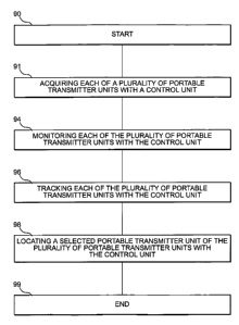
parent unit 44. In the exemplary method, control then proceeds to an optional
operation 98, where a selected child unit of the child units 44 is located
using the
parent unit 42. Control proceeds to 99, where the method ends.
Figure 23 illustrates operations performed during initialization of the parent
unit 42 in accordance with the exemplary embodiment of the invention. The
method
begins at 101 and control proceeds to 102. At 102, the power is latched on
(i.e., by
pressing the power button S6, S7 of the parent unit 42), the imports are
initialized,
and the frequency synthesizer 72 is set up. Control then proceeds through
blank
node 103 to 104, at which a determination is made whether the power button
(S6,
S7) has been released. If the power button is released, the ID codes 46 may be
randomly generated and control proceeds directly to 106. If not, control
proceeds to
blank node 103. At 106, the parent unit 42 runs a self test and control
proceeds to
108. At 108, the parent unit 42 selects an operating channel using the
frequency
synthesizer 72 and the RSSI level and chirps through the speaker 71. Control
then
proceeds to 110, where a power conservation operation is performed.
Figures 24 and 25 illustrate the power down operation that is performed in
the parent unit 42. The power down operation begins at 112 and control
proceeds to
113. At 113, a determination is made whether the power button (S6, S7) has
been
depressed. If the power button (S6, S7) has been depressed, control proceeds
directly to 118. If not, control proceeds directly to 114. At 114, a
determination is
made whether one of the child switches has been depressed. If one of the child
switches has been depressed, control proceeds directly to 116 through blank
node
CA 02441054 2003-09-15
WO 02/073559 PCT/US02/07512
115. If not, control proceeds directly to 160. At 116, a determination is made
whether the child switch has been released. If the child switch is released,
control
proceeds to 130. If not, control proceeds to blank node 115.
At 118, after the power button (S6, S7) or the child switch has been
5 depressed, a determination is made whether the speaker 71 or audible is on.
If the
audible is on, control proceeds directly to 120. If not, control proceeds to
121. At
120, the speaker 71 is turned off and muted. Control then proceeds to blank
node
121. From blank node 121, control proceeds to 122, where a determination is
made
whether the parent unit 42 exceeds a predetermined time limit. If the parent
unit 42
10 does exceed the turn-off limit, then control proceeds to 124. If not,
control proceeds
to 112, where the power conservation operation begins. At 124, the parent unit
42
chirps through the speaker 71 and sends power down message to any active child
units 44. Control proceeds to 126, at which the parent unit 42 chirps through
the
speaker 71 and shuts down circuitry 50. The status check operation 130 is
illustrated
1 S in Figure 27 and the operation 160 is illustrated in Figs. 28, 29 and 30.
Figures 26 and 27 illustrate operations performed during a status check in
accordance with the exemplary embodiment of the invention. The operations
begin
at 131 and control proceeds to 132. At 132, it is determined whether a child
unit is
acquired. If so, the parent unit 42 chirps through speaker 71 and control
proceeds to
20 160. If not, control proceeds to 150, as will be described in greater
detail below. At
134, a determination is made whether one of the child units 44 is in track by
the
parent unit 42. If so, control proceeds directly to 136. If not, control
proceeds
directly to 142. At 136, the parent unit 42 is set to normal mode and to full
power.
Control proceeds directly to 138, at which the parent unit 42 sends normal
poll
25 command or message to the child unit 44. Control proceeds to 140, at which
a
determination is made whether the child unit 44 has responded to the poll
message.
If so, the parent unit 42 chirps through speaker 71 and control proceeds to
160. If
not, control proceeds to 137. At 142, the microprocessor unit 510 of the
parent unit
42 is set to track mode and the speaker 71 is turned off. Control proceeds
directly to
30 144, at which the parent unit 42 is set to full power and sends a track
command or
message to the child unit 44. Control then proceeds to 146, at which a
determination
CA 02441054 2003-09-15
WO 02/073559 PCT/US02/07512
31
is made whether the child unit 44 has responded to the track message. If so,
control
proceeds to 148 the parent unit 42 chirps through speaker 71 and control
proceeds to
300. If not, control proceeds to 147. This process is repeated up to five (5)
times at
which time control is passed to 300.
At 150 in Figure 27, the operations performed during acquire mode in
accordance with the exemplary embodiment of the invention are illustrated. The
operations 150 begin at 151 and control proceeds to 152. At 152, the parent
unit 42
is set to full power and sends an acquire command or message to the child unit
44.
Control proceeds to 154, at which a determination is made whether the child
unit 44
has responded to the acquired message. If so, control proceeds directly to
156. If
not, control proceeds to 151. At 156, the microprocessor unit 510 of parent
unit 42
is set to acquire mode and control proceeds directly to 160.
Figure 28 illustrates operations 160 performed during polling mode in
accordance with the exemplary embodiment of the invention. The operations 160
begin at 161. Control proceeds to 162, at which the parent unit 42 reads a
range
switch and control proceeds to 164. At 164, a determination is made whether a
child
unit 44 and the parent unit 42 are in track with one another. If so, control
proceeds
directly to 240. If not, control proceeds to 166. At 166, a determination is
made
whether the first child unit 44 is acquired. If so, control proceeds to 168.
If not,
control proceeds to 190. At 168, the parent unit 42 sends a normal poll
command or
message to the first child unit 44 and control proceeds to 170. At 170, a
determination is made whether the first child unit 44 has responded to the
normal
poll message. If so, control proceeds to 178. If not, control proceeds to 172.
At
172, an error count, i.e., number of successive missed polls, of the child
units 44
monitored by the parent unit 42 is bumped upward by one count. Polls may be
missed because the child unit 44 does not respond to the parent unit or
because the
response from the child unit 44 does not reach the parent unit 42, i.e., the
distance
between the child unit 44 and the parent unit 42 is too far. Control proceeds
to 174,
at which a determination is made whether the parent unit 42 is over the error
count
limit. If so, the parent unit 42 sets a perimeter alarm, turns on an audible,
and sets
up an LED. If not, control proceeds to 190.
CA 02441054 2003-09-15
WO 02/073559 PCT/US02/07512
32
At 178, a determination is made whether the first child unit 44 has a low
battery using low battery detection circuit 74. If so, control proceeds to
180. At
180, a low battery flag is set and control proceeds to 190. If not, control
proceeds to
182. At 182, a determination is made whether the response from the first child
unit
S 44 is a panic command or message. If so, control proceeds to 183. At 183,
the
panic mode is set and an LED is activated. Control then proceeds to 190. If
not,
control proceeds to 184. At 184, a determination is made whether the response
of
the first child unit 44 is a normal poll acknowledgment response. If not,
control
proceeds to 190. If so, control proceeds to 186. At 186, the parent unit 42
resets the
error count, i.e., which is the number of successive missed polls, and turns
off the
perimeter alarm being generated through the speaker 71.
Figure 29 illustrates operations performed during polling of the second child
unit in accordance with the exemplary embodiment of the invention. Operations
illustrated in Figure 29 with respect to the second child unit 44 that are
similar to
those described above for the first child unit 44 are given identical
reference
numerals and are not commented further upon. Control proceeds to 191 from
blank
node 190. At 191, which is similar to 166 in Figure 28, a determination is
made
whether the second child unit 44 is acquired by the parent unit 42. If so,
control
proceeds to 168 and the description above relating to the first child unit 44
will
suffice to give an understanding of the second child unit 44 as well. If not,
control
proceeds to 192.
Figure 30 illustrates operations performed during polling of the third child
unit 44 in accordance with the exemplary embodiment of the invention. The
operations begin at 192 and control proceeds to 193. At 193, it is determined
whether a third kit unit 44 is acquired by the parent unit 42. If so, control
proceeds
directly to 194. If not, control proceeds to 220. At 194, the parent unit 42
sends a
normal poll command or message to the third child unit 44. Control then
proceeds
to 196, at which a determination is made whether the third child unit 44 has
responded to the normal poll message. If so, control proceeds to 204. If not,
control
proceeds to 198. At 198, the error count of the child units 44 monitored by
the
parent unit 42 is bumped upward by one count and control proceeds to 200. At
200,
CA 02441054 2003-09-15
WO 02/073559 PCT/US02/07512
33
a determination is made whether the error count is over the predetermined
error
count limit, i.e., number of successive missed polls. If not, control proceeds
to 220.
If so, control proceeds to 202. At 202, the parent unit 42 sets the perimeter
alarm,
turns on an audible, and sets up the LED. Control then proceeds to 220. At
204, it
is determined whether the response from the third child unit 44 signals a low
battery
using the low battery detection circuit 74. If so, control proceeds to 206. At
206,
the parent unit 42 sets a low battery flag and control proceeds to blank node
221. If
the response from the third child unit 44 did not signal a low battery,
control
proceeds to 208. At 208, it is determined whether the response from the third
child
unit 44 was a panic response. If not, control proceeds through blank node 229
to
230. If so, control proceeds to 210, at which the parent unit 42 sets panic
mode and
activates an LED in the housing 48. Control then proceeds to blank node 221.
At
230, it is determined whether the response is a normal poll acknowledgment
response. If so, control proceeds to blank node 221. If not, control proceeds
to 232.
At 232, the error count is reset and the sound generator or alarm is turned
off.
Control then proceeds through blank node 221 to 220.
At 220, it is determined whether alarm conditions are present, such as, for
example, a child button being pressed. If so, control proceeds to 222. If
alarm
conditions are not met, control proceeds to 224. At 224, the parent unit 42
reads its
battery power and control proceeds to 225. At 225, it is determined whether
the
battery power of the parent unit 42 is low. If so, control proceeds to 226. If
not,
control proceeds to 227. At 226, the parent unit 42 sets the battery as low
and may
light a LED to indicate that the battery is low. At 227, the parent unit 42
may chirp
or set an audio signal through the speaker 71 as required. Control then
proceeds to
110.
Figure 30 illustrates operations performed during tracking mode in
accordance with the exemplary embodiment of the invention. The operations
begin
at 241 and control proceeds to 242. At 242, the parent unit 42 sets up the
antenna
switching, as described above, and control proceeds to 250. At 250, a
determination
is made whether a child button, i.e., one of the keybutton LEDs 59, has been
pushed.
If not, control proceeds to 262. At 262, the power of the parent unit 42 is
set to full.
CA 02441054 2003-09-15
WO 02/073559 PCT/US02/07512
34
Control then proceeds to 264, at which a normal poll message is sent. Control
then
proceeds to 266, at which a determination is made whether the parent unit 42
has
received a response from the child units 44. If not, control proceeds to 260.
If so,
control proceeds to 268. At 268, the parent unit 42 is set to its normal mode
and
control then proceeds to 110. If a child button has been pushed, control
proceeds to
300 (Figure 34).
At 300 the parent unit 42 reads the RSSI signal strength until a suitable
value
is obtained. Control is then passed to 304. At 304 the first antenna is
selected and the
circuit is tuned by adjusting the D/A until a maximum value from the output of
the
detector 632 is obtained. The proper analog value is saved and set up in the
D/A
circuit. At 314 antenna #2 is set and the same procedure is used for
detector output 634. Control proceeds through blank node 326 Figure 34.
Control is then passed to 270. At 270, the parent unit 42 reads the PHASE DET
and control proceeds to 272. At 272, a determination is made whether the
analog
value indicates left, right or center. If the value is left, control proceeds
to 274. At
274, the left counter is bumped and control proceeds to 281. If not, control
proceeds
to 276. At 276, a determination is made whether the child unit is positioned
to the
right of the parent unit 42. If so, control proceeds to 278, at which the
direction
finder right counter is bumped. Control then proceeds to 281. If not, control
proceeds to 280. At 280, the direction finder is bumped to the center and
control
proceeds to 281. At 281, a determination is made whether the parent unit 42
has
performed 4000 reads. If not, control proceeds to 250. If so, control proceeds
to
290.
Figure 34 At 290, control proceeds to 292. At 292, it is determined whether
the center voltage is the greatest. If so, control proceeds to 293. At 293,
the center
LED is displayed and control proceeds to 250. If the center is not the
greatest,
control proceeds to 294. At 294, it is determined whether the right voltage is
the
greatest. If so, control proceeds to 295. At 295, the right LED is displayed
and
control proceeds to 250. If the right voltage is not the greatest, control
proceeds to
296. At 296, the left LED is displayed and then control proceeds to 250.
CA 02441054 2003-09-15
WO 02/073559 PCT/US02/07512
Figure 35 illustrates operations performed during power up sequence of the
child unit 44 in accordance with the exemplary embodiment of the invention.
The
operations begin at 300 and control proceeds to 302. At 302, the power is
latched
on, the ports are initialized, acquire mode is set and the frequency
synthesizer 710
5 (Figures 3 and 14) is set up. Control then proceeds to 303. At 303, a blank
node
allows control to proceed to 304, at which a determination is made whether the
power button (S8, S9) has been released. If the power button (S8, S9) is
released,
control proceeds directly to 306. If not, control proceeds to 303. At 306, the
child
units 44 may chirp through speaker 71 to acknowledge that the power button (S8
or
10 S9) has been released and control proceeds to 308 through blank node 307.
At 308,
the child unit 44 is set to receive mode and a watchdog is set, where the
child unit 44
looks for signals transmitted from the parent unit 42. Control then proceeds
to 310
through a blank node 309. At 310, it is determined whether there is a
synchronization, i.e., using the clocks 57 of the respective microprocessor
units 720,
15 510 of child unit 44 and the parent unit 42. If not, control proceeds to
blank node
309. If so, control then proceeds to 314, at which the child unit 44 reads the
ID code
46, reads the assigned kid number which the child unit 44 has been assigned to
by
the parent unit 42, and reads commands or messages from the parent unit 42.
Control proceeds to blank node 316.
20 In Figure 36, control proceeds from the blank node 316 to 318. At 318, it
is
determined whether the poll command or message transmitted from the parent
unit
42 is valid. If not, control proceeds to blank node 307. If so, control then
proceeds
directly to 320. At 320, it is determined whether the parent unit 42 is trying
to detect
the direction of the child unit 44. If so, control proceeds to operation 321.
If not,
25 control then proceeds directly to 322. At 322, it is determined whether the
child unit
44 is in acquire mode, and whether the command from the parent unit 42 is
assign.
If not, control proceeds to 324. If so, control proceeds to 323, at which the
child unit
44 confirms the assignment to the parent unit 42 and also sets a timeout to
conserve
power, whereby the circuit 54 will power down after a predetermined amount of
30 inactivity. Control then proceeds to blank node 325.
CA 02441054 2003-09-15
WO 02/073559 PCT/US02/07512
36
At 324, it is determined whether the ID codes 46 and the child numbers
transmitted from the parent unit 42 compare to those assigned to each of the
child
units 44. If not, control proceeds to blank node 307. If so, control proceeds
to 326,
at which it is determined whether the command transmitted from the parent unit
42
is search. If so, control proceeds to operation 321. If not, control proceeds
to 328,
at which it is determined whether the command transmitted from the parent unit
42
is normal poll, whereby the parent unit 42 transmits and receives one signal
to each
of the child units 44. If not, control proceeds to blank node 330. If so,
control then
proceeds to operation 329.
Figure 37 shows control proceeding from blank node 330 to 332. At 332, it
is determined whether the command transmitted from the parent unit 42 is power
down. If so, control proceeds to 334. If not, control proceeds directly to
336. At
334, the child unit 44 transmits a normal response to the parent unit 42 and
shuts
down. At 336, it is determined whether the command transmitted from the~parent
unit 42 is change channel. If not, control proceeds to blank node 325. If so,
control
proceeds to 338. At 338, the child unit 44 responds to the parent unit 42 that
the
command is confirmed and the child unit 44 changes to a selected channel,
which
may be selected, for example, by implementing the method illustrated in Figure
23
via the frequency synthesizers 520, 710. Control then proceeds to 340, at
which a
valid poll is set by the child unit 44. Control proceeds directly to 342. At
342, it is
determined whether the poll was valid. If not, control proceeds to blank node
307.
If so, control proceeds to 325.
Figure 38 illustrates control proceeding from blank node 325 to 344. At 344,
the battery voltage of the child unit 44 is read and control proceeds to 346.
At 346,
it is determined if the battery is low, for example, using the low battery
detection
circuit 74. If so, control proceeds to 348, at which a low battery flag is
set, and
control proceeds to blank node 349. If not, control proceeds to blank node
349.
From blank node 349, control proceeds to 350. At 350, the status of the
proximity
switch (i.e., the proximity detection circuit 84 or the water detection
circuit 85) is
checked and control proceeds to 352. At 352, it is determined whether the
proximity
switch has been tripped. If not, control proceeds to 356. If so, control
proceeds to
CA 02441054 2003-09-15
WO 02/073559 PCT/US02/07512
37
354. At 354, the panic mode is set and the speaker 71 is turned on. Control
then
proceeds to blank node 307. At 356, it is determined whether the predetermined
time limit has expired. If so, control proceeds to 358 where the child units
44 are
shut down. If not, control proceeds to blank node 307.
S Figure 39 illustrates the operation 329. The operation 329 begins at blank
node 359. Control then proceeds from the blank node 359 to 360. At 360, it is
determined whether the child unit 44 is in panic mode via pressing the help
button
(S9). If so, control proceeds to 361. If not, control proceeds to 362. At 361,
the
child unit 44 transmits a panic response to the parent unit 42 and control
then
proceeds to blank node 307. At 362, it is determined whether the parent unit
42 is in
direction detection mode. If so, control proceeds to 364. If not, control
proceeds to
366. At 364, the mode is cleared, the child unit 44 responds normally to the
parent
unit 42 and control then proceeds to blank node 307. At 366, it is determined
whether the unit is in normal mode. If not, control proceeds to 368. If so,
control
proceeds to 370. At 368, a normal response is transmitted to the parent unit
42 and
control then proceeds to blank node 307. At 370, it is determined whether a
low
battery flag has been set. If not, a normal response is transmitted to the
parent unit
42 and control then proceeds to blank node 307. If so, control proceeds to
374, at
which a low battery response is transmitted to the parent unit 42 and control
then
proceeds to blank node 307. When control proceeds to blank node 307 from
either
361, 364, 368 or 372, the operation 329 ends.
Figure 40 further illustrates operation 321. The operation 321 begins at
blank node 375 and control proceeds from blank node 375 to 376. At 376, the
antenna 80 in the child unit 44 is set for continuous wave output, the search
mode of
the child unit 44 is set and control proceeds directly to blank node 377. From
blank
node 377, control proceeds to 378. At 378, it is determined whether the child
unit
44 is "window time", whereby the child unit 44 searches for commands or
messages
transmitted from the parent unit 42, such as those described above. If so,
control
proceeds to blank node 307 and the operation 321 ends. If not, control
proceeds to
blank node 377.
CA 02441054 2003-09-15
WO 02/073559 PCT/US02/07512
38
As described above, the parent unit 42 continuously polls the child units 44
and may select a different operating channel at any time to avoid interference
with
other apparatuses 40. That way, the child units 44 are less likely to become
lost ox
to lose communication with the parent unit 42.
After the user finishes using the device 40, the parent unit 42 and the child
units 44 may be powered off and stored until the next usage as described
above.
While the principles of the invention have been made clear in the illustrative
embodiments set forth above, it will be apparent to those skilled in the art
that
various modifications may be made to the structure, arrangement, proportion,
elements, materials, and components used in the practice of the invention.
It will thus be seen that the objects of this invention have been fully and
effectively accomplished. It will be realized, however, that the foregoing
preferred
specific embodiments have been shown and described for the purpose of
illustrating
the functional and structural principles of this invention and are subject to
change
without departure from such principles. Therefore, this invention includes all
such
modifications.