Note: Descriptions are shown in the official language in which they were submitted.
CA 02441124 2011-06-22
rL.l!UaUL/V/3 l1
WO 02/076164
ELECTRONIC MODULE WITH FLUID DISSOCIATION ELECTRODES AN.
METHODS
Field of the Invention
The present invention relates to the field of electronic modules, and, more
particularly, to electronic modules including a substrate for cooling one or
more
electronic devices and associated methods.
Background of the Invention
Electronic devices are widely used in many types of electronic equipment, One
electronic device is the integrated circuit which may include a silicon or
gallium
arsenide substrate and a number of active devices, such as transistors, etc.
formed in an upper surface of the substrate. It is also typically required to
supp rt
one or more such integrated circuits in a package that provides protection and
permits external electrical connection.
As the density of active devices on typical integrated circuits has increased,
dissipation of the heat generated has become increasingly more important. In
particular, a relatively large amount of heat may be generated in multi-chip
modules (MCMs), microwave transmitters, and photonic devices, for example.
One device which has been used in a variety of applications, including
electroni i
circuit modules, to provide high thermal transport over long distances is the
so-
called "heat pipe." A heat pipe is a sealed system that includes an
evaporator, a
condenser, an adiabatic region connecting the evaporator and condenser for
liquid and vapor transport, and a capillary or wick for circulating cooling
fluid
therein. Heat pipes enjoy an advantage over other forms of heat regulating
devices in that they can transfer heat without the need for a mechanical pump,
compressor or electronic controls, which may provide space savings in certain
instances.
An example of an MCM which uses a heat pipe is disclosed in U.S. Patent No.
5,216,580 to Davidson et al. entitled "Optimized Integral Heat Pipe and
Electronic
Module Arrangement." This MCM includes electronic circuit components
1 --
CA 02441124 2003-09-10
WO 02/076164 PCT/US02/07312
-2-
mounted on one side thereof and a thermal wick mounted on
another side. A heat pipe evaporator and condenser assembly is
attached to the MCM and wick assembly. Furthermore, a suitable
working fluid is introduced into the heat pipe assembly which
is then hermetically sealed.
Of course, cooling devices generally need to be on the
same size scale as the electronic devices they are intended to
cool. Yet, the benefits associated with heat pipes are subject
to scaling limitations. That is, ever increasing packaging
densities, which put high power devices in close proximity with
conventional circuitry, may require that larger amounts of heat
be transferred more quickly than is possible using conventional
heat pipe assemblies not having a pump.
Summary of the Invention
In view of the foregoing background, it is therefore an
object of the invention to provide an electronic module and
related methods which provides adequate cooling of one or more
electronic devices and has relatively small dimensions.
This and other objects, features, and advantages in
accordance with the present invention are provided by an
electronic module including a cooling substrate, an electronic
device mounted thereon, and a plurality of cooling fluid
dissociation electrodes carried by the cooling substrate for
dissociating cooling fluid to control a pressure thereof. The
cooling substrate may have an evaporator chamber adjacent the
electronic device, at least one condenser chamber adjacent the
heat sink, and at least one cooling fluid passageway connecting
the evaporator chamber in fluid communication with the at least
one condenser chamber.
More particularly, the electronic module may drive the
plurality of cooling fluid dissociation electrodes, for
example, by sensing a temperature thereof and driving the
plurality of cooling fluid dissociation electrodes responsive
to the sensed temperature. The plurality of cooling fluid
dissociation electrodes may also allow cooling fluid
dissociation during manufacture of the electronic module. Each
of the cooling fluid dissociation electrodes may include metal,
and the metal is preferably resistant to corrosion from the
CA 02441124 2003-09-10
WO 02/076164 PCT/US02/07312
-3-
cooling fluid. For example, the metal may include at least one
of gold and nickel.
Furthermore, the electronic module may also include a
heat sink adjacent the cooling substrate. The plurality of
cooling fluid electrodes may include an evaporator thermal
transfer body connected in thermal communication between the
evaporator chamber and the electronic device and at least one
condenser thermal transfer body connected in thermal
communication between the at least one condenser chamber and
the heat sink. The evaporator thermal transfer body each and
the at least one condenser thermal transfer body may have a
higher thermal conductivity than adjacent cooling substrate
portions. Further, the evaporator thermal transfer body and the
at least one condenser thermal transfer body may have thermal
conductivities greater than about 100 Watts per meter-degree
Celsius.
Moreover, the evaporator thermal transfer body, the at
least one condenser thermal transfer body, and the at least one
cooling fluid passageway may cause fluid flow during operation
of the electronic module without a pump. The evaporator thermal
transfer body may include a wicking portion exposed within the
evaporator chamber for facilitating cooling fluid flow by
capillary action. Also, the at least one condenser thermal
transfer body may include at least one wicking portion exposed
within the at least one condenser chamber for facilitating
cooling fluid flow by capillary action.
Additionally, the cooling substrate may further include
projections extending inwardly into the at least one cooling
fluid passageway for facilitating cooling fluid flow by
capillary action. The cooling substrate may also include
projections extending inwardly into the evaporator chamber and
the at least one condenser chamber for facilitating cooling
fluid flow by capillary action.
A method aspect of the invention is for controlling
cooling fluid pressure in an electronic module including a
cooling substrate and an electronic device carried by the
cooling substrate. The cooling substrate includes an
evaporator chamber, at least one condenser chamber, and at
least one cooling fluid passageway connecting the evaporator
chamber in fluid communication with the at least one condenser
CA 02441124 2003-09-10
WO 02/076164 PCT/US02/07312
-4-
chamber. Further, the electronic device is carried by the
cooling substrate adjacent the at least one condensor chamber.
The method includes driving a plurality of cooling fluid
dissociation electrodes carried by the cooling substrate for
dissociating cooling fluid to control a pressure thereof.
Brief Description of the Drawings
FIG. 1 is a perspective view of an electronic module
according to the present invention.
FIG. 2 is a cross-sectional view taken along line 2-2 of
FIG. 1.
FIG. 3 is an exploded perspective view of a cooling
substrate in accordance with the invention.
FIG. 4 is a top view of the evaporator thermal transfer
body of the electronic module of FIG. 2.
FIG. 5 is a side view of the evaporator thermal transfer
body of the electronic module of FIG. 2.
FIG. 6 is a perspective view of the condenser thermal
transfer body of the electronic module of FIG. 2.
FIG. 7 is a top view of the condenser thermal transfer
body of the electronic module of FIG. 2.
FIG. 8 is a side view of the condenser thermal transfer
body of the electronic module of FIG. 2.
FIG. 9 is a graph of modeled heat transfer capacity
versus groove or capillary wick width for the electronic module
of FIG. 1.
FIG. 10 is a graph of modeled device temperature versus
a number of thermal vias used in the electronic module of FIG.
1.
FIG. 11 is a graph of junction temperature versus power
dissipated for the electronic module of FIG. 1.
Detailed Description of the Preferred Embodiments
The present invention will now be described more fully
hereinafter with reference to the accompanying drawings, in
which preferred embodiments of the invention are shown. This
invention may, however, be embodied in many different forms and
should not be construed as limited to the embodiments set forth
herein. Rather, these embodiments are provided so that this
disclosure will be thorough and complete, and will fully convey
CA 02441124 2003-09-10
WO 02/076164 PCT/US02/07312
-5-
the scope of the invention to those skilled in the art. Like
numbers refer to like elements throughout. The dimensions of
layers and regions may be exaggerated in the figures for
greater clarity.
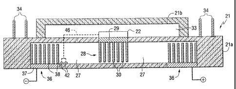
Referring initially to FIGS. 1-8, the electronic module
20 in accordance with the invention is now initially described.
The electronic module 20 includes a package 21 surrounding an
electronic device 22. The package 21 includes a base or
cooling substrate 21a and a lid 21b connected thereto. The lid
21b defines a cavity 33 over the electronic circuit 22 for
protection of the electronic circuit and its interfaces (not
shown). The lid 21b may be attached by brazing using a seal
ring, for example, as will be appreciated by those of skill in
the art, though other configurations are also possible. The
package 21 may include low temperature co-fired ceramic (LTCC)
material, for example. This material offers advantages in
terms of ruggedness, and an ability to form recesses and small
stable passageways therein, as well as to provide electrical
paths therethrough. Of course, other similar materials may be
used as well.
In other embodiments, two or more electronic devices 22
may be carried by the package 21, as will be appreciated by
those skilled in the art. The electronic device 22 may include
semiconductor devices or integrated circuits, heat coils,
resistors, etc., for example. Of course, other electronic
devices may also be included in the electronic module 20. The
package 21, as best seen in FIG. 1, may carry electrical
connectors 34 on at least one of its surfaces. For example,
the electrical connectors 34 may be pins in a pin grid array,
as illustratively shown. In other embodiments, edge connectors
may be provided to connect to a ribbon type cable, for example,
as will be appreciated by those skilled in the art.
A heat sink 23 is adjacent the cooling substrate 21a and
may include fins 24, for example. Of course, other heat sinks
known to those of skill in the art may also be used. For
example, the heat sink maybe a rack or metal chassis in which
the electronic module is mounted. Further, the heat sink and
one or more condenser thermal transfer bodies (described below)
may be formed as a single homogenous body. The cooling
substrate 21a also has an evaporator chamber 25 adjacent the
CA 02441124 2003-09-10
WO 02/076164 PCT/US02/07312
-6-
electronic device 22, at least one condenser chamber 26
adjacent the heat sink 23, and at least one cooling fluid
passageway 27 connecting the evaporator chamber in fluid
communication with the at least one condenser chamber. The
total area of the condenser chambers 26 may be made grater than
that of the evaporator chamber 25 to reduce heat flux entering
the fins (or heat sink) 24. This may be particularly desirable
to do for electronic devices 22 that get so hot that even
direct attachment to a heat sink would be insufficient to
properly cool the device.
In the embodiment illustrated in FIG. 3, the cooling
substrate 21a includes four condenser chambers 26 and four
cooling fluid passageways 27 extending radially outward from
the evaporator chamber 25 in a configuration resembling an "X".
Of course, those of skill in the art will appreciate that any
number of cooling fluid passageways and condenser chambers may
be used without departing from the scope of the present
invention.
The electronic module 20 further includes an evaporator
thermal transfer body 28 connected in thermal communication
between the evaporator chamber 25 and the electronic device 22.
Furthermore, a condenser thermal transfer body 36 is connected
in thermal communication between each condenser chamber 26 and
the heat sink 23. Of course, it will appreciated that more
than one heat sink 23 may be used in accordance with the
invention.
The evaporator thermal transfer body 28 and the
condenser thermal transfer bodies 36 each preferably have
thermal conductivities greater than about 100 Watts per-meter
degree Celsius. The thermal transfer bodies 28, 36 may also
have a higher thermal conductivity than adjacent portions of
the cooling substrate 21a. Those skilled in the art will
appreciate that the thermal transfer bodies 28, 36 allow a low
operating temperature of the electronic device 22 to be
maintained, as illustrated in FIG. 10.
By way of example, the evaporator thermal transfer body
28 and the condenser thermal transfer bodies 36 may include at
least one of a copper-graphite composite material, AlSiC, and
metal. Of course, other suitable materials known to those of
skill in the art may also be used, and it is preferred that the
CA 02441124 2003-09-10
WO 02/076164 PCT/US02/07312
-7-
material used be resistant to corrosion from the cooling fluid
(e.g., at least one of nickel and gold). It is anticipated
that both thermal transfer bodies 28, 36 will be used in
accordance with the present invention to maximize cooling fluid
flow. Yet, it should be understood that both thermal transfer
bodies may not be necessary in every application and that one
or the other may be used.
As a result, the evaporator thermal transfer body 28,
the condenser thermal transfer bodies 36, and the cooling fluid
passageways 27 cause cooling fluid flow during operation of'the
electronic module without a pump. Moreover, the various
materials noted above that are used for the cooling substrate
21a and the thermal transfer bodies 28, 36 are all reasonably
matched in temperature coefficient of expansion (CTE) (a
material property) with each other and semiconductor materials.
This matching allows for direct mounting of silicon and other
electronic devices 22 to the cooling substrate 21a. For
example, the cooling substrate 21a may be an LTCC and the
thermal transfer bodies 28, 36 may be a copper-graphite
composite material.
To enhance the cooling fluid flow, the evaporator
thermal transfer body 28 includes a wicking portion exposed
within the evaporator chamber 25 for facilitating cooling fluid
flow by capillary action. The wicking portion includes a
plurality of projections 30 extending outwardly from a base
plate 29. The plurality of projections 30 may be arranged in a
generally rectangular pattern, as shown in FIGS. 4 and 5,
although other configurations may also be used. The base plate
29 facilitates sealing with adjacent cooling substrate 21a
portions, as will be described further below.
Likewise, each condenser thermal transfer body 36 also
includes at least one wicking portion exposed within its
respective condenser chambers 26 for facilitating cooling fluid
flow by capillary action.
3.5 The wicking portion includes a base 45 and a plurality
of projections 38 extending outwardly therefrom. The
projections 38 may be arranged in two generally rectangular
groups oriented at a substantially right angle, as illustrated
in FIGS. 6 and 7. Also, the condenser thermal transfer body 36
may further include a base plate 37 for facilitating sealing
CA 02441124 2003-09-10
WO 02/076164 PCT/US02/07312
-8-
with adjacent cooling substrate 21a portions, as will be
described further below. Each of the projections 38 may
include a reduced width tip portion 39 to alleviate capillary
flooding by increasing the gap distance therebetween. This
facilitates the removal of a thermally impeding fluid layer and
thus promotes condensation. The condenser thermal transfer
bodies 36 may also include a reservoir portion 40 adjacent the
wicking portion defining a cooling fluid reservoir.
Further, to enable cooling fluid flow return to the
evaporator chamber 25, the cooling substrate 21a may also
include projections 41 extending inwardly into the cooling
fluid passageways, the evaporator chamber, and the condenser
chambers 26 defining respective wicking surfaces for
facilitating cooling fluid flow by capillary action. That is,
a high flow rate capillary is formed with a high surface energy
that provides internal full surface coverage and allows for
rapid fluid transport. This alleviates capillary depletion
which otherwise may occur on non-wicking surfaces, which may be
particularly important in small heat pipe assemblies.
The projections 41 may be created, for example, by
forming interconnecting orthogonal grooves on adjacent cooling
substrate 21a layers on opposing parallel surfaces of the
cooling fluid passageways 27 and chambers 25, 26. Processes
used to create these structures are based on standard
multilayer ceramic fabrication techniques known to those of
skill in the art. Of course, those skilled in the art will
appreciate that other wicking structures may also be used in
accordance with the present invention.
In addition, a plurality of fluid dissociation
electrodes may be carried by the cooling substrate 21a to
control a pressure of the cooling fluid. In one embodiment,
any two of the thermal transfer bodies 28, 36 may be used as
the fluid dissociation electrodes and may be driven by
differing (e.g., positive and negative) DC potentials (see FIG.
2), for example, to cause dissociation of cooling fluid. In an
alternative embodiment, fluid dissociation electrodes 42 may be
mounted within the cooling substrate 21a. By causing cooling
fluid to dissociate into its constituent gases, the fluid
dissociation electrodes allow the pressure, and thus the flow
rate, of the cooling fluid to be controlled. That is, the
CA 02441124 2003-09-10
WO 02/076164 PCT/US02/07312
-9-
partial pressure of the dissociated gases are increased, which
thereby decreases the partial pressure of the fluid vapor and
increases the operating temperature. When the fluid
dissociation electrodes are used, the cooling fluid is
preferably one that may be dissociated when a current is passed
therethrough, for example, water.
In one embodiment, the fluid dissociation electrodes
allow dissociation of cooling fluid during the manufacturing
process. In another embodiment, the electronic device 22 may
drive the fluid dissociation electrodes 42 (or the thermal
transfer bodies), for example, by sensing a temperature of the
electronic device and driving the electrodes responsive to the
sensed temperature, as illustratively shown with a dashed
connection line 46 in FIG. 2. Each of the fluid dissociation
electrodes 42 may be metal which, again, is preferably
resistant to corrosion from the cooling fluid. The electrodes
42 may therefore also include at least one of gold and nickel.
Of course, it will be appreciated by those skilled in the art
that the fluid dissociation electrodes 42 may be used in a
variety of structures other than the cooling substrate
disclosed herein.
The electronic module 20 may be fabricated as a multi-
layer ceramic structure as follows. Unfired (green) ceramic in
tape form is processed to cut the required cavities and wick
structures. Internal thick film conductors are then printed as
required to route the multi-level circuitry. Once the
individual layers are complete, they are stacked and laminated
to form a green body which is then fired. Singulation of
individual structures may then be performed, if necessary, by
diamond sawing or other suitable methods. Lapping may be
required to remove surface deformations produced during
lamination and firing, as will be appreciated by those of skill
in the art.
Post-fired thick film conductors are then printed and
fired to provide the base plates 29, 37 to provide brazeable,
sealing surfaces for the evaporator and condenser thermal
transfer bodies 28, 36, respectively. The base material for
the thermal transfer bodies 28, 36 (e.g., a copper-graphite
composite material) may then be nickel and gold plated for.
brazing to the LTCC cooling substrate 21a. The brazing process
CA 02441124 2003-09-10
WO 02/076164 PCT/US02/07312
-10-
is preferably fluxless to avoid contamination of the wicking
surfaces and provides hermetic sealing of the cooling substrate
21a.
Fine leak verification may be used to ensure package
integrity, as will be appreciated by those skilled in the art.
It may also be necessary to attach the electronic device 22
prior to filling the cooling substrate 21a with cooling fluid
to allow for solder die to attach to the thermal transfer
bodies 28, 36. Otherwise, a filled, operational heat pipe may
inhibit reflow or catastrophically fail if internal vapor
pressures become to high. A fill tube, such as a copper tube,
may be included in the cooling substrate 21a for evacuation and
filling. The filling may be accomplished by injection.
Those of skill in the art will appreciate that numerous
advantages are provided according to the present invention.
For example, the enhanced capillary flow achieved according to
the present invention may allow for miniature cooling fluid
channel dimensions believed to be previously unavailable in the
prior art. Also, the fluid reservoir 40 and evaporator thermal
transfer body 28 incorporating the wicking portion reduces the
effect of pool boiling and extends the power density upper
limit.
Moreover, the condenser thermal transfer body 36
promotes clearing of the condensate (liquid) from the
condensing surface to provide substantially continuous
unimpeded condensation. Also, designs including a central or
multiple evaporator chambers 25 and one or more condenser
chambers 26 interconnected by one or more cooling fluid
passageways 27 for the routing of cooling fluid are also
provided by the present invention. This enables dense
packaging of large heat flux devices and stabilizes the
temperature of multiple components at identical temperatures.
Additionally, as noted above, the dissociation electrodes 42
allow for gas generation and, consequently, regulation of
pressure and operating temperature.
The preceding advantages may be more fully appreciated
with reference to the test results provided in the following
example of an electronic module fabricated according to the
present invention.
CA 02441124 2003-09-10
WO 02/076164 PCT/US02/07312
-11-
EXAMPLE
The design of the electronic module 20 according to the
present invention accommodates heat spreading away from the
electronic device 22 as well as temperature stable operation,
as will be appreciated by those of skill in the art. Spreading
is accomplished by increasing the condenser area with respect
to that of the evaporator and by dividing and separating the
condenser from the evaporator. For example, a test electronic
module according to the present invention was constructed to
have a-total condenser area of about twice that of the
evaporator area, although other dimensions may also be used
according to the invention.
Each segment of the heat pipe structure defined by the
cooling substrate 21a has unique considerations, several of
which relate to scaling limitations. The most notable
limitation is that such "miniature" heat pipes are more
sensitive to vapor-liquid interaction through the adiabatic
region than their larger counterparts. Vapor flow can be
dramatically restricted if certain characteristic dimensions
are not maintained. For the test device described herein, it
was determined that a minimum vapor channel cross section of
1.27 mm was required, though smaller dimensions may be possible
according to the present invention in other designs, as will be
understood by those of skill in the art.
A low partial pressure of any unintended gasses should
be maintained to avoid reducing the partial pressure of the
vapor formed from the desired cooling fluid. Miniature heat
pipes are very sensitive to unintended gasses, and thus
hermetic sealing is preferred. Furthermore, the wicking
surfaces 41 should provide a fine enough structure to prevent
condensation droplets from forming and depleting the cooling
fluid supply. Additionally, cooling fluid should come in close
contact with the heat sources to enable temperature stable
device operation, and condensation surfaces should remain clear
of a thermally impeding fluid layer. Moreover, capillary flow
should be unimpeded with sufficient capacity, and a condenser-
to-evaporator ratio should be sufficiently higher than one.
The choice of cooling fluid is also important as it should be
free of contaminants, especially dissolved gasses. Water was
chosen for the cooling fluid in the test device because of its
CA 02441124 2008-11-05
high latent heat of evaporation, well-understood properties, and ease of
degassing by boiling, of course, other cooling fluids may also be used.
Other design parameters may also need to be taken into account. For
example, some of the key geometric parameters include the cross-sectional
structure of the cooling fluid passageways 27 and length of the wicking
surfaces 41. Others parameters include the evaporator and condenser
chamber 25, 26 sizes and structures, which may be driven by empirical
results and fabrication issues, as will be understood by those of skill in the
art.
io These parameters drive the size of the device required to provide a given
heat dissipation capacity for a given type and number of electronic devices
22. Further discussion of such design parameters with respect to the present
invention may be found in a paper entitled "Miniature Embedded Heat Pipes
in Low Temperature Co-Fired ceramic for Electronic Devices Requiring
Temperature Stability," by the applicants of the present invention which was
presented at the Society of Automotive Engineers Aerospace Power Systems
Meeting on November 1, 2000, in San Diego, California.
Generally speaking, the capillary-action pump is the limiting factor in heat
transport capability. One of the key parameters for capillary pumping is the
width, of the grooves used to define the projections 41 and resulting wicking
surfaces. This parameter is important because it drives the capillary limit to
supply cooling fluid to the evaporator chamber 25. The groove width should
be carefully chosen to account for sag and layering requirements, as will be
appreciated by those of skill in the art. The groove width chosen for the test
device (about 4 mils) was selected based upon materials and fabrication
issues, including considerations of total substrate thickness. Guidance from
the modeling discussed further in the above referenced paper was also used.
A curve showing the optimization of heat transport due to the capillary end
vapor friction resulting from variation of the groove width may be seen in
FIG.
10.
Another key parameter of importance is the heat transport length from the
heat source (i.e., electronic device 22) to the evaporator 25. This is
important
for the
12
CA 02441124 2008-11-05
effectivity of the cooling substrate 21 a to maintain a moderately low
temperature on the electronic device 22 requiring the heat dissipation. The
electronic device 22 should Interface with the evaporator chamber 25 with as
little thermal reactivity as possible. As such, it is preferable that any
material
used underneath the electronic device 22 be vacuum sealable to the LTCC
and matched in CTE, as discussed above.
A simplified model may be used to illustrate thermal resistivity of the LTCC
cooling substrate 21 a with thermal vias 35 for conduction to the evaporator
io chamber 25. The model includes a thermal path through a substrate of the
electronic device 22 and the cooling substrate 21 a with thermal vias 35
(each of which has its own thermal resistivity) and terminating in an
idealized
constant-temperature evaporator chamber.
Based upon this model, while the evaporator may function at around 45 deg
C the source device temperature may be significantly higher depending on
the materials and geometry, as may be seen in the graph of FIG. 10. The
independent variable represents the number of thermal vias 35 in the path
directly beneath the electronic device 22. The graph also illustrates that the
electronic device 22 temperature cannot be maintained at a constant value
versus heat load if there is significant thermal resistivity in the thermal
path.
Thermal resistivity is particularly important if the goal is to eliminate
thermal
electric coolers from the system. With an ambient environment the goal is
typically to keep electronic devices operating as close to ambient as
possible.
With the above design considerations in mind, the test device was fabricated
to include four condenser chambers 26 and four cooling fluid passageways
27 connecting respective condenser chambers to the evaporator chamber 25.
Each of the cooling fluid passageways was made 9.5 mm in length, though
longer or shorter lengths are possible according to the present invention.
Again, a small hole was formed on the top side of the electronic module 20
just over one of the condenser chambers 26 and a copper fill tube was also
brazed therein to allow evacuation and filling of the cooling fluid.
The thermal transfer bodies 28, 36 were mounted to allow direct coupling to
the respective wicking surfaces 41. The
13
CA 02441124 2008-11-05
thermal transfer bodies 28, 36 were hermetically brazed to the LTCC cooling
substrate 21 a using 80/20 gold/tin. An Ultra _FETTm Power metal oxide
semiconductor field effect transistor (MOSFET) bare die (0.28 cm) made by
the assignee of the present invention was used as the electronic device 22.
This MOSFET was solder mounted adjacent the evaporator chamber 25 and
wire bonded to a thick film surface metallization forming the base plate 29 to
provide electrical interconnect. Wires soldered to the same metallization
provided interconnection to an
electrical test fixture.
As noted above, the cooling substrate 21 a may be LTCC. LTCC is a
commercially available low temperature firing glass-ceramic (850 deg C)
system originally developed for multi-layered circuit fabrication which can
accommodate high conductivity metal circuits (such as gold, silver, and
copper) and hermetic packaging. Typical properties of the tape noted above
include a thermal conductivity between 2 and 3 W/mK and a CTE of
7ppm/deg C. High thermal conductivity thermal transfer bodies 28 36 with a
CTE matched to that of the LTCC were used to seal the heat pipes at the
evaporator and condenser chambers 25, 26, and 80/20 Gold/Tin solder was
used to provide hermeticity.
In order to test the device, several pieces of test equipment were used
including a DC power supply, a custom power control circuit, a thermoelectric
cooler, and two .003" wire type K thermocouples with temperature meters.
The custom power control circuit allowed for independent control of the
MOSFET power utilizing feedback circuitry, and the thermoelectric cooler was
used to maintain a stable condenser temperature. The thermoelectric cooler
was maintained at 20 C throughout the test to provide a stable condenser
chamber 26 temperature which aided measurement taking and calculations.
One of the two thermocouples was used to measure the condenser
temperature, and the other was placed in contact with the MOSFET surface
with the aid of thermal grease which allowed continuous junction temperature
monitoring. All tests were conducted horizontally in still air.
Test units fabricated as described above were tested over a range of 10
Watts of heat dissipation. The results may be seen in the graph shown in
FIG. 11. The graph illustrates a junction temperature runaway that results
when the substrate is
45
14
CA 02441124 2008-11-05
passive (i.e., unfilled) (line 46) versus an active operating substrate (line
47).
A hysteresis reference line 48 is also provided. The thermal heat pipe cycle
activated at about 3 Watts and stabilized at about 6 Watts. This range of
parameters may be ideal for many electronic devices or other systems
requiring reduced power dissipation and reduced circuit complexity. More
specifically, the present invention is therefore suitable for use with laser
diode
arrays, computer central processing unit (CPU) chips, radio frequency (RF)
power modules, high density multi-chip nodules, optical modules, and
phased array antennas, for example.
Many modifications and other embodiments of the invention will come to the
mind of one skilled in the art having the benefit of the teachings presented
in
the foregoing descriptions and the associated drawings. Therefore, it is to
be understood that the invention is not to be limited to the specific
embodiments disclosed, and that other modifications and embodiments are
intended to be included within the scope of the appended claims.