Note: Descriptions are shown in the official language in which they were submitted.
CA 02441173 2003-09-15
WO 02/075446 PCT/GB02/01199
1
APPARATUS FOR PROVIDING
TIMING JITTER TOLERANT OPTICAL MODULATION
OF A FIRST SIGNAL BY A SECOND SIGNAL
Field of the Invention
This invention relates to optical modulators, which incorporate pulse-shaping
fibre
Bragg gratings, and which are tolerant to timing jitter.
Background of the Invention
In order to `synthesize' a particular optical pulse form one needs to be able
to
reliably define the amplitude and phase profile of an optical field. The
general approach is
to generate pulses with a well-defined pulse form and to then pass the pulse
through some
pulse shaping element with an appropriately designed transfer function to re-
phase and re-
shape the incident spectrum so as to obtain the desired output optical field.
The pulse-
shaping element can have a pure linear response such as a filter with a
suitably complex
response, or might additionally include a non-linear element, e.g. an optical
fibre or an
aperiodic quasi-phase matched structure, to allow the controlled generation of
frequency
components outside the frequency spectrum of the input pulse-form.
The most commonly used technique is a simple linear filtering technique in
which
the frequency components of a short pulse are spatially dispersed using bulk
gratings, and
then filtered by means of amplitude and phase-masks positioned within a
Fourier optical 4f
set-up. Microlithographically fabricated spatial-masks, segmented liquid
crystal
modulators, or acousto-optic modulators have been used as spatial filters, the
latter two
approaches allowing for programmability and dynamic reconfigurability of the
pulse
shaping response. Whilst impressive results are possible with this approach,
the hardware
CA 02441173 2003-09-15
WO 02/075446 PCT/GB02/01199
2
itself is somewhat bulky, lossy and expensive and does not lend itself to
ready integration
with waveguide devices. These issues have prompted the search for other
technical
approaches to the problem such as the use of arrayed waveguide gratings, and
arrays of
fibre delay lines.
Single channel data rates approaching the Tbit/s level have now been reported
for
optical time division multiplexing (OTDM) systems. These single channel data
rates place
increased demands and tolerances on the techniques used to multiplex and
demultiplex the
optical data bits. Consider for example the case of optical demultiplexing. As
OTDM data
rates increase, and the pulses used get correspondingly shorter, the
synchronization
requirements placed on the locally generated pulses used to control the switch
operation
can become a limiting practical issue. The key to reducing time jitter
tolerance in such
devices is to establish a rectangular temporal switching window. This reduces
the absolute
accuracy for temporal bit alignment and provides optimal resilience to timing
jitter-induced
errors. Fibre based non-linear optical loop mirror (NOLM) demultiplexing
schemes that
provide both good, ultra-fast performance and tolerance to timing jitter of
either or both of
the control and data signals have been demonstrated previously. These schemes
use the
difference in group velocity and the resultant `walk-off ` between the control
and data
signals within the non-linear optical device to define the rectangular
switching window.
This consequently requires tight specification and control of both the data
and signal
wavelengths, and the dispersion characteristics of the fibre. Whilst this
approach is
applicable to fibre based switches, it is complex and cannot be applied to
switches based
on highly non-linear semiconductors and within which there are no appreciable
dispersive
propagation effects over the length scales of relevance. Simple, robust
techniques that can
CA 02441173 2003-09-15
WO 02/075446 PCT/GB02/01199
3
help reduce time jitter tolerances and that are applicable to a variety of
switching
mechanisms are thus of great interest.
It is an aim of the present invention to obviate or reduce the above mentioned
problems.
Summary of the Invention
According to one non-limiting embodiment of the present invention, there is
provided apparatus for providing timing jitter tolerant optical modulation of
a first signal
by a second signal, the first signal having a first wavelength, the second
signal comprising
a plurality of second signal pulses having a second pulse shape and a second
wavelength,
and the apparatus comprising a first signal input port, a second signal input
port, a coupler,
a grating and a non-linear optical device, the apparatus being configured to
direct the
second signal at the second signal input port to the non-linear optical device
via the coupler
and the grating, and to direct the first signal at the first signal input port
to the non-linear
optical device; the grating being a superstructured fibre Bragg grating that
converts the
second signal pulses into intermediary pulses each having an intermediary
pulse shape; and
the intermediary pulse shape being such that it provides a switching window
within the
non-linear optical device.
The first signal can comprise a plurality of first signal pulses. The first
signal can
be a continuous wave signal such as an un-modulated laser beam. The switching
window
can be rectangular, Gaussian, or any other user-defined shape.
In one embodiment of the invention, the first signal comprises a plurality of
first
signal pulses, the grating is defined by a grating impulse response, the
intermediary pulse
CA 02441173 2003-09-15
WO 02/075446 PCT/GB02/01199
4
shape is defined by the convolution of the second pulse shape and the grating
impulse
response, and the switching window is a substantially rectangular switching
window which
provides tolerance to a variation in arrival time of the first signal pulse at
the first input
port and the second signal pulse at the second input port substantially equal
to the width of
the rectangular switching window.
In another embodiment of the invention, the first signal comprises a plurality
of
first signal pulses each having a width, the grating is defined by a grating
impulse response,
the intermediary pulse shape is defined by the convolution of the second pulse
shape and
the grating impulse response, the grating being such that the intermediary
pulse shape is a
substantially rectangular pulse, and in which the apparatus has a tolerance to
a variation in
arrival time of the first pulse at the first input port and the pulse at the
second input port
substantially equal to the width of the substantially rectangular pulse minus
the width of
the first signal pulse.
The apparatus of the invention may be one in which the coupler is a
circulator. The
coupler may be an optical fibre coupler.
The apparatus may comprise an optical switch, the optical switch being such
that it
comprises the non-linear optical device.
The non-linear optical device may be a holey fibre. The holey fibre may
comprise
glass. The glass may be silica, a silicate glass, or a compound glass.
Alternatively, the
holey fibre may comprise a polymer.
The holey fibre may comprise a core and a cladding, in which the cladding
comprises a plurality of holes arranged around the core, and in which the core
has a
CA 02441173 2003-09-15
WO 02/075446 PCT/GB02/01199
diameter less than lOum. The core may have a diameter less than 5um. The core
may have
a diameter less than 2um.
The holey fibre may comprise a dopant, the dopant being selected from the
group
comprising Ytterbium, Erbium, Neodymium, Praseodymium, Thulium, Samarium,
Holmium Dysprosium, Tin, Germanium, Phosphorous, Aluminium, Boron, Antimony,
Uranium, Gold, Silver, Bismuth, Lead, a transition metal, and a semiconductor.
The above
list of elements includes associated chemical compounds of the element, and in
particular
all-oxide forms.
The non-linear optical device may be, or may comprise, a semiconductor optical
amplifier.
The non-linear optical device may comprise a lithium niobate channel
waveguide,
or a lithium niobate planar waveguide.
The non-linear optical device may comprise a periodically poled lithium
niobate
channel waveguide or a periodically poled lithium niobate planar waveguide.
The non-linear optical device may be an optical switch, a holey fibre, a poled-
fibre,
a potassium titanyl phosphate (KTP) or other crystalline waveguide, a
periodically poled
KTP or other crystalline waveguide, a non-linear optical loop mirror, a Kerr
gate, an
optical fibre, a non-linear amplifying loop mirror, or a non-linear optical
modulator.
The optical non-linearity used within the non-linear optical device may be
based on
second-order (x(2)), or third-order (x(3)) non-linear effects. The specific
manifestation/use
of the non-linearity might be in terms of Self-Phase Modulation (SPM), Cross-
Phase
Modulation (CPM), Four-Wave Mixing (FWM), parametric frequency conversion,
second
CA 02441173 2003-09-15
WO 02/075446 PCT/GB02/01199
6
harmonic generation, third harmonic generation, sum frequency generation,
difference
frequency generation, supercontinuum generation, cascaded second order
effects, or some
combination thereof. Other optical non-linearites that might be used include
Raman and
Brillouin effects, cross gain modulation and two photon absorption.
The apparatus may be configured to modulate the first signal.
The apparatus may be configured to demultiplex the first signal.
The apparatus may comprise an actively mode-locked fibre laser.
The apparatus may comprise an interferometer comprising a first arm and a
second
arm, and in which the first arm comprises the non-linear optical device.
The apparatus may comprise a filter, and in which the filter is a wavelength
selective filter.
The apparatus may comprise a polarizing element, and in which the polarizing
element is a polarizer or a polarization beam splitter.
The apparatus may comprise a clock generator. The clock generator may be a
short-pulse generator selected from the group comprising a mode-locked fibre
laser, an
actively mode-locked fibre laser, a generator comprising an electro-absorption
modulator
and a laser, a generator comprising an electro-optic modulator and a laser,
and a gain-
switched laser diode.
The clock generator may comprise a means for pulse compression such as
dispersion compensator fibre, a chirped fibre Bragg grating, a dispersion
decreasing fibre,
an optical amplifier, a Raman amplifier, an optical switch, an optical pulse
compressor, or
some combination of these devices.
CA 02441173 2003-09-15
WO 02/075446 PCT/GB02/01199
7
The apparatus may comprise a plurality of non-linear optical devices and be
configured to direct the second signal at the second signal input port to each
of the non-
linear optical devices. The apparatus may be configured as an optical
multiplexer. The
apparatus may be configured as an optical demultiplexer. The apparatus may be
configured as an inverse multiplexer. The apparatus may comprise a switch and
a control
input for controlling the switch.
Brief Description of the Drawings
Embodiments of the invention will now be described solely by way of example
and
with reference to the accompanying drawings in which:
Figure 1 shows apparatus according to the present invention for providing
jitter
tolerant optical modulation of a first signal by a second signal;
Figure 2 shows an embodiment of the present invention in which the
intermediary
pulse shape is defined by the convolution of the second pulse shape and the
grating impulse
response;
Figure 3 shows a grating impulse response;
Figure 4 shows an intermediary pulse shape;
Figure 5 shows a substantially square switching window;
Figure 6 shows a first signal pulse arriving prior to a second signal pulse;
Figure 7 shows a first signal pulse arriving after a second signal pulse;
Figure 8 shows the impulse response of an optical switch;
CA 02441173 2003-09-15
WO 02/075446 PCT/GB02/01199
8
Figure 9 shows an embodiment of the present invention configured to provide a
substantially rectangular pulse;
Figure 10 shows a grating impulse response;
Figure 11 shows an embodiment comprising an optical switch;
Figure 12 shows the end face of a holey fibre;
Figure 13 shows apparatus according to the present invention and comprising a
holey fibre;
Figure 14 shows apparatus according to the present invention and comprising an
interferometer;
Figure 15 shows apparatus according to the present invention configured as an
optical demultiplexer;
Figure 16 shows apparatus according to the present invention and configured as
an
optical multiplexer;
Figure 17 shows apparatus according to the present invention and configured as
an
inverse multiplexer;
Figure 18 shows apparatus according to the present invention and further
comprising a switch;
Figure 19 shows a multiplexer according to the present invention with
regenerative
properties;
Figure 20 shows a DWDM multiplexer according to the present invention;
CA 02441173 2003-09-15
WO 02/075446 PCT/GB02/01199
9
Figure 21 shows apparatus according to the present invention utilizing
continuous
wave switching;
Figures 22 to 30 show the results of calculation on pulse shaping filters
according
to the present invention;
Figure 31 shows apparatus according to the present invention comprising a mode
locked ring laser;
Figures 32 to 39 show experimental and theoretical results on the performance
of a
rectangular pulse shaping filter according to the present invention;
Figure 40 shows a test set up for characterizing apparatus according to the
present
invention;
Figures 41 to 44 show theoretical and experimental performance of apparatus
according to the present invention;
Figure 45 shows a test set up for characterizing apparatus comprising a
semiconductor optical amplifier according to the present invention;
Figures 46 and 47 shows experimental results for the semiconductor optical
amplifier;
Figure 48 shows a definition of a switching window; and
Figure 49 shows a typical transmission response of a fibre-based non-linear
optical
device.
CA 02441173 2003-09-15
WO 02/075446 PCT/GB02/01199
Detailed Description of Preferred Embodiments of the Invention
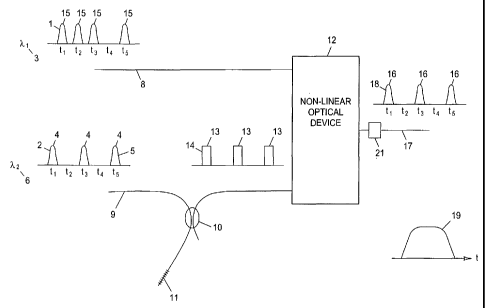
Figure 1 shows apparatus for providing timing jitter tolerant optical
modulation of a
first signal 1 by a second signal 2. The first signal 1 has a first wavelength
3. The second
signal 2 comprises a plurality of second signal pulses 4 having a second pulse
shape 5 and
a second wavelength 6. The apparatus further comprises a first signal input
port 8, a
second signal input port 9, a coupler 10, a grating 11 and a non-linear
optical device 12.
The apparatus is configured to direct the second signal 2 at the second signal
input port 9 to
the non-linear optical device 12 via the coupler 10 and the grating 11, and to
direct the first
signal 1 at the first signal input port 8 to the non-linear optical device 12.
The grating 11 is
a superstructured fibre Bragg grating that converts the second signal pulses 4
into
intermediary pulses 13 each having an intermediary pulse shape 14. The
intermediary
pulse shape 14 is such that it provides a switching window 19 within the non-
linear optical
device 12.
The switching window 19 may be a substantially rectangular switching window 50
shown with reference to Figure 5. The switching window 19 may be alternatively
be
Gaussian, or any other user-defined shape.
The apparatus can be configured such that the apparatus has a single optical
input
port so that first and second signals 1 and 2 enter the apparatus through the
same input port.
The apparatus may further comprise a filter 21 as shown in Figure 1.
The coupler 10 can be a circulator, an optical fibre coupler or a beam
splitter.
The first signal 1 is shown as comprising a plurality of first signal pulses
15. These
first signal pulses 15 interact with the intermediary pulses 13 within the non-
linear optical
CA 02441173 2003-09-15
WO 02/075446 PCT/GB02/01199
11
device 12, providing an output signal 18 comprising a plurality of output
pulses 16 at the
output port 17. The first signal 1 is shown as having pulses in time slots tl,
t2, t3 and t5;
the second signal 2 is shown as having pulses in time slots tl, t3 and t5; and
the output
signal 18 is shown as having pulses in time slots tl, t3 and t5 - ie
corresponding to the
overlap in time of the first signal pulses 15 and the intermediary pulses 13
within the non-
linear optical device 12. The substantially rectangular switching window 50
provided by
the intermediary pulse shape 14 helps to reduce distortion of the first signal
pulses 15
within the non-linear optical device 12 and provides tolerance to jitter in
the arrival times
of the first signal pulses 15.
Although Figure 1 shows the first signal 1 as comprising a plurality of first
signal
pulses 15, the first signal 1 can alternatively be a continuous wave signal
such as an un-
modulated laser beam.
The first wavelength 3 can be different from the second wavelength 6. In this
case,
the non-linear optical device 12 is preferably a semiconductor active element
or an optical
fibre such as the holey fibre 120, and the filter 21 is preferably a
wavelength selective filter
such as a fibre Bragg grating or a thin-film filter.
The first wavelength 3 can be the same as the second wavelength 6. In this
case,
the non-linear optical device 12 is preferably such that its output state of
polarization
changes in response to the intermediary pulses 13, and the output filter 21 is
preferably a
polarizer or a polarizing beam splitter.
The first signal 1 can be a data signal and the second signal 2 can be a clock
signal.
In this case the apparatus provides a demultiplexing function. Alternatively,
the first signal
1 can be a clock signal and the second signal 2 can be a data signal whereupon
the
CA 02441173 2003-09-15
WO 02/075446 PCT/GB02/01199
12
apparatus provides a multiplexing function.
Figure 2 shows one embodiment of the invention in which the first signal 1
comprises a plurality of first signal pulses 15. The grating 11 is defined by
a grating
impulse response 30 as shown in Figure 3. As shown in Figure 4, the
intermediary pulse
shape 14 is defined by the convolution of the second pulse shape 5 and the
grating impulse
response 30. The grating impulse response 30 is selected to provide the
rectangular
switching window 50 shown in Figure 5 in the non-linear device, 12, which in
Figure 2 is
shown as comprising a semiconductor optical amplifier 20.
The apparatus may further comprise the filter 21.
The semiconductor optical amplifier 20 can be part of a terahertz optical
assymetric
demultiplexer (TOAD), semiconductor laser amplifier in a loop mirror (SLALOM),
an
ultra-fast non-linear interferometer (UNI), a gain transparent ultra-fast non-
linear
interferometer (GT-UNI).
The rectangular switching window 50 provides tolerance to a variation in
arrival
time of the first signal pulse 15 at the first input port 8 and the second
signal pulse 4 at the
second input port 9 substantially equal to the width 51 of the rectangular
switching window
50 minus the width of the first signal pulse 15.
Figure 6 shows an example in which the first signal pulse 15 arrives at a time
61,
the second signal pulse 4 arrives at a time 62, and in which the rectangular
switching
window is the width 51. Figure 7 shows another example in which the first
signal pulse 15
arrives at a time 71, the second signal pulse 4 arrives at a time 72, and in
which the
rectangular switching window is the width 51. Figures 6 and 7 illustrate the
maximum
CA 02441173 2003-09-15
WO 02/075446 PCT/GB02/01199
13
possible variation in the arrival times 61 and 62 such that the non-linear
optical device 12
does not distort the first signal pulse 15 by virtue of timing jitter.
The term switching window can be defined in a number of ways. A first
definition
shown in Figure 21 is that the `continuous wave switching window' 210 is
defined by the
pulse shape 210 when driven by the intermediary pulse 13 in response to the
second signal
pulses 4, and in which the first signal 1 at wavelength 3 is a continuous wave
beam. When
using the apparatus with a first signal 1 comprising first signal pulses 15,
the switching
window is given by the width of the `continuous wave switching window' 210
minus the
width of the first signal pulse 15. A second definition can be couched more
directly in
terms of the system performance itself as illustrated in Figure 48 which shows
a plot of Bit
Error Rate (BER) 480 versus relative time delay 481 of the pulses associated
with the first
and second signal pulses 15, 4. Bit error rate measurements provide a measure
of the
quality of the pulse switching provided by the apparatus, the higher the bit
error rate the
worse the switch performance. An error rate of 1 in 10-9 is often referred to
as error-free
and taken to represent the lower bound on acceptable performance of
telecommunication
apparatus. Thus an alternative system description of timing window for the
switch is the
total length of relative timing delay 482 over which error free performance
can be
achieved. The BER increases rapidly at the rising and trailing edges of the
timing window.
In practice the two definitions of timing values give roughly equivalent
values under the
two definitions, particularly for rectangular switching windows and we use
both definitions
herein. More specifically we tend to use the first definition when the
intermediary pulse
form is itself substantially rectangular in shape, and the later definition
for the more general
case.
CA 02441173 2003-09-15
WO 02/075446 PCT/GB02/01199
14
The embodiment shown in Figure 2 is representative of switching approaches in
which the required intermediary pulse form required to provide a substantially
rectangular
switching window is not a rectangular pulse, but some other pulse form that
compensates
for non-instantaneous non-linear responses (such as cross gain modulation) and
dispersive
effects within the non-linear optical device 20.
In order to establish the intermediary pulse shape 14 it is necessary first to
characterise the impulse response 80 shown in Figure 8 of the non-linear
optical device 12
as a function of incident pulse energy/power, and then to use this information
to establish
the required form of intermediary pulse shape 14 needed to define a
substantially
rectangular switching window 50. The impulse response 30 of the grating I I
required to
convert the second signal pulses 4 can then be evaluated, and the required
supestructured
grating design itself derived using a suitable inverse grating design
algorithm such as R.
Feced, M.N. Zervas, and M.A. Muriel, "An efficient inverse scattering
algorithm for the
design of non-uniform fibre Bragg gratings", IEEE J. Quantum Electron.,
vol.35, pp:I 105-
1111, 1999.
In order to determine the impulse response 80 of the non-linear optical device
12
(as a function of incident pulse power) it may be necessary to use an
experimental pulse
characterisation technique capable of providing both phase and amplitude
information.
Appropriate techniques are described in B.C. Thomsen, P. Petropoulos, H!L.
Offerhaus,
D.Y. Richardson, and J.D. Harvey, "Characterization of a 10 GHz harmonically
mode-
locked erbium fibre ring laser using second harmonic generation frequency
resolved optical
gating", Technical Digest CLEO'99, Baltimore, 23-28 May 1999, paper CTuJS.
Further
means to provide such characterisation are found described in "Measuring
ultrashort laser
CA 02441173 2003-09-15
WO 02/075446 PCT/GB02/01199
pulses in the time domain using frequency resolved optical gating" by R.
Trebino, KW
DeLong, DN Fittinghoff, JN Sweetser, MA Krumbugel, BA Richman, DJ Kane in
Review
of Scientific Instruments, Vol. 68, 3277-3295, (1997).
Also shown in Figure 2 is a filter 21 that may be necessary for filtering the
output
of the non-linear optical device 12. The filter 21 may be a polarising element
such as a
polarizer or a polarization beam splitter, a wavelength selective filter such
as an optical
fibre Bragg grating or thin film filter. When used in conjunction with a
semiconductor
optical amplifier as shown in Figure 2, the filter 21 is preferably a
wavelength selective
filter.
Figure 9 shows another embodiment of the invention in which the first signal 1
comprises a plurality of first signal pulses 15. The grating 11 is defined by
a grating
impulse response 100. As shown in Figure 10, the intermediary pulse shape 14
is defined
by the convolution of the second pulse shape 5 and the grating impulse
response 100. The
grating 11 being such that the intermediary pulse shape 14 is a substantially
rectangular
pulse 95, and in which the apparatus has a tolerance to a variation in arrival
time of the first
pulse 15 at the first input port 8 and the second pulse 4 at the second input
port 9
substantially equal to the width 101 of the substantially rectangular pulse 95
minus the
width of the first signal pulse 15. The non-linear optical device 12 shown in
Figure 9 is a
non-linear loop mirror (NOLM) 90 comprising dispersion shifted optical fibre
(DSF) 91
and two couplers 92. The couplers are preferably 3dB optical fibre couplers.
The DSF 91
is configured to have normal dispersion at the first wavelength 3 and may have
a length in
the region 1 in to 10,000m depending on the amount of non-linearity present.
The NOLM
90 may further comprise a polarization controller 93. The first wavelength 3
is different
CA 02441173 2003-09-15
WO 02/075446 PCT/GB02/01199
16
from the second wavelength 6. The first wavelength 3 is usually at a shorter
wavelength
than the second signal wavelength 6 for fibre based devices since: (a) it is
often important
to minimise group velocity induced walk-off between the first and intermediary
signal
pulses 15, 13 as they propagate through the nonlinear fibre and this is most
readily
achieved by arranging the two signal wavelengths to lie roughly symmetrically
about the
zero dispersion wavelength of the fibre, and (b) the switched, or modulated
signal 1 needs
to lie in the normal dispersion regime in order to avoid the impact of induced
intensity
noise due to soliton effects. The filter 21 is preferably a wavelength
selective filter, which
may be a fibre Bragg grating or a thin-film filter.
The tolerance to difference in arrival times, and thereby jitter, of the first
and
second optical signals 1 and 2 is determined by the widths 50 and 101 of the
substantially
rectangular switching window 50 or the substantially rectangular pulse 95
respectively. It is
envisaged that using suitably fabricated gratings 11 this tolerance could be
as large as
200ps. This tolerance is suitable for high jitter tolerance optical processing
at data rates as
low as 5 Gbit/s. At the other extreme we envisage that the technology should
also allow
the generation of intermediary pulses 13 with widths as short as 100fs, making
it suitable
for optical processing at data rates between I Thit/s to at least 10 Thit/s.
The technology
should also allow processing at intermediate date rates.
Figure 11 shows an embodiment in which the apparatus comprises an optical
switch
111, the optical switch 111 being such that it comprises the non-linear
optical device 12.
The optical switch 111 can be used in each of the embodiments shown in Figures
1, 2 and
9. The non-linear optical device 12 may comprise a lithium niobate channel
waveguide, or
a lithium niobate planar waveguide. The non-linear optical device 12 may
comprise a
CA 02441173 2011-08-30
17
periodically poled lithium niobate channnel waveguide or a periodically poled
lithium
niobate planar waveguide. The non-linear optical device may comprise a holey
fibre, a
poled-fibre, a potassium titanyl phosphate (KTP) or other crystalline
waveguide, a
periodically poled KTP or other crystalline waveguide, a non-linear optical
loop mirror, a
Kerr gate, an optical fibre, a non-linear amplifying loop mirror, or a non-
linear optical
modulator.
Figure 12 shows the cross-section of a holey fibre 120 which can be configured
as
the non-linear optical device 12 in the embodiments of Figures 1, 2 and 9. The
holey fibre
120 comprises a core 121 and a cladding 122, in which the cladding 122
comprises a
plurality of holes 125 arranged around the core 121. The holey fibre 120 has a
core
diameter 123 of 2 m. Thecore 121 and the cladding 122 are shown enlarged in
the inset.
The core 121 can have a diameter 123 between 2 m and 10 m. Preferably the core
121
has a diameter 123 less than 2 m. By holey fibre, we mean a fibre comprising
longitudinally-extending holes that may be twisted along the length of the
fibre and we
include similar or alternatively-named fibres such as microstructured fibres
and photonic
band-gap fibres.
The holey fibre 120 is made from a single transparent material 124
(discounting
air as a constituent material). The transparent material 124 is silica. Holey
fibres can also
be made from other forms of silicate glass (e.g Lead glasses such as Schott
glasses
SF57, SF58, SF59, or Bismuth oxide based glasses), or indeed any other form of
glass
including any compound glass (eg multi-component glasses such as chalcogenide
glasses). Preferably, the glass would have a large third order (Kerr) non-
linear coefficient
(.2.10-20m2/W ), and low loss at the operating wavelength of the non-linear
optical device
DOCSTOR: 2248922\1
CA 02441173 2003-09-15
WO 02/075446 PCT/GB02/01199
18
(<10 dB/m). The material may also be a polymer, such as polymethyl
methacrylate
(PMMA) although any polymer with a significant second order (>0.01 pm/V), or
third
order non-linear coefficient (>2.10-20 m2/W) could be envisaged. The holey
fibre 120 may
also comprise a dopant in either the core 121 or the cladding 122, or both.
The dopant may
comprise Ytterbium, Erbium, Neodymium, Praseodymium, Thulium, Samarium,
Holmium
Dysprosium, Tin, Germanium, Phosphorous, Aluminium, Boron, Antimony, Uranium,
Gold, Silver, Bismuth, Lead, a transition metal, and a semiconductor.
Figure 13 shows an apparatus comprising the holey fibre 120 and coupling means
131 for coupling optical energy into and out of the holey fibre 120. The
length of the holey
fibre 120 can be between 0.1m and 10km. The dispersion can be normal or
anamalous at
the first signal wavelength 3. In certain instances it is preferable for the
dispersion to be
normal at the first signal wavelength 3 and anomalous at the second signal
wavelength 6 to
minimise pulse walk-off. Normal dispersion for the first signal wavelength is
advantageous in order to avoid soliton induced noise effects. In other
instances it may be
desirable to have both the first and second signal wavelengths 3, 6 in the
normal dispersion
regime in order to avoid soliton-induced intensity noise effects.
Figure 14 shows an apparatus comprising an interferometer 140 comprising a
first
arm 141 and a second arm 142. The first arm 141 comprises the non-linear
optical device
12. The interferometer 140 is a Mach Zehnder interferometer. The apparatus can
also be
constructed using a Michelson Interferometer, a Sagnac interferometer or
another
configuration of optical interferometer.
Figure 15 shows an apparatus configured as an optical demultiplexer 1500. The
apparatus de-multiplexes the first signal 1 into a plurality of lower data
rate signals 157.
CA 02441173 2003-09-15
WO 02/075446 PCT/GB02/01199
19
The apparatus comprises a clock generator 151, couplers 152, a plurality of
the non-linear
optical devices (NOD) 12 and the filters 21 interconnected by first optical
fibres 153 and
second optical fibres 154. The first and second optical fibres 153, 154 have
lengths
configured such that the non-linear optical devices 12 demultiplex the first
optical signal 1
into different ones of the lower data rate signals 157. It is preferable that
the clock
generator 151 is synchronized to the first optical signal 1 utilizing a tap
150 which may be
an optical coupler. In the example shown, the clock generator 151 will output
a second
optical signal 2 having a frequency four times less than the frequency of the
first optical
signal 1. The filters 21 have filter output ports 155 that are shown connected
to optical
communication lines 156 that may comprise at least one optical amplifier 158.
The clock generator 151 may comprise a short-pulse generator. The short pulse
generator can be a mode-locked fibre laser, an actively mode-locked fibre
laser, a generator
comprising an electro-absorption modulator and a laser, a generator comprising
an electro-
optic modulator and a laser, a gain-switched laser diode. The short-pulse
generator may
also comprise a means for pulse compression such as dispersion compensator
fibre, a
chirped fibre Bragg grating, a dispersion decreasing fibre, an optical
amplifier, a Raman
amplifier, an optical switch, an optical pulse compressor, or some combination
of these
devices.
Figure 16 shows an apparatus configured as an optical multiplexer 1600. The
apparatus multiplexes a plurality of first optical signals 1 into a higher
data rate signal 161.
The apparatus comprises a multiplexer 160, an output port 162, and a plurality
of optical
fibres 161. The optical fibres 161 have lengths configured such that the non-
linear optical
devices 12 multiplex the first optical signals 1 into the higher data rate
signal 161 without
CA 02441173 2003-09-15
WO 02/075446 PCT/GB02/01199
cross-talk. It is preferable that the clock generator 151 is synchronized to
at least one of the
first optical signals 1 utilizing a tap 150 which may be an optical coupler.
In the example
shown, the clock generator 151 will output a second optical signal 2 having a
frequency
four times greater than the frequency of the first optical signal 1. The
apparatus may
further comprise a wavelength converter for converting the wavelength of one
or more of
the first optical signals 1.
Figure 17 shows an apparatus configured as an inverse multiplexer 1700. The
inverse multiplexer demultiplexes a first optical signal 1 into a plurality of
lower data rate
signals 179 having different wavelengths for transmission through a wavelength
division
multiplexed (WDM) optical transmission line 172. This application has
advantages for
demultiplexing a 40Gb/s signal into four 10Gb/s signals operating on four
wavelength
channels in a WDM system. The optical transmission line 172 may be between
I00m and
a thousand kilometres in length, and may comprise at least one optical
amplifier 158. The
demultiplexing stage 1701 is similar to the apparatus shown in Figure 15
except that the
lower data rate signals 179 have different wavelengths. The apparatus
therefore contains
wavelength converters 170 configured such that the lower data rate signals 179
have
different wavelengths from each other. The wavelength converters are shown
connected to
the second optical fibres 154. They can also be connected to the first optical
fibres 153 or
the filters 21. Alternatively, they be an integral part of the non-linear
optical devices 12.
The wavelength converters 170 may comprise a semiconductor amplifier, a NOLM,
a
dispersion shifted fibre, an optical fibre, a holey fibre, or a lithium
niobate device.
CA 02441173 2003-09-15
WO 02/075446 PCT/GB02/01199
21
The lower data rate signals 179 are multiplexed with a multiplexer 171 into a
wavelength division multiplexed signal 178 which is transmitted through a
wavelength
division multiplexed optical transmission line 172.
The multiplexing stage 1702 following the optical transmission line 172 is
similar
to the apparatus of Figure 16 except that it comprises a wavelength division
demultiplexer
173 that demultiplexes the lower data rate signals 179. The multiplexing stage
1702 may
be exchanged with an electronic multiplexer.
The inverse multiplexer 1700 may require dispersion compensators to balance
the
overall group delays between the different wavelength channels propagating
through the
optical transmission line 172. Differential delays may also be required
between the
different wavelength channels in order to reconstitute the first signal 1
properly at the
output 162. The differential delays may be introduced by taking great care in
the optical
path lengths in the demultiplexing stage 1701 and the multiplexing stage 1702.
Differential delays may also be added electronically at the receiver utilizing
some form of
pattern recognition on the received data.
Figure 18 shows an apparatus comprising a control line 180 and a switch 181.
The
control line 180 may be an optical control line 180 and the switch 181 may be
an optical
switch. The switch 181 can also be located on the first optical input 8 or
connected to the
filter 21. The apparatus is useful for turning the non-linear optical device
12 on and off
and can be used to provide intelligent routing of optical signals through
optical
telecommunication networks. The apparatus shown in Figure 18 can be
incorporated in
any of the embodiments of the invention described above, for example in order
to add
intelligence into an optical network.
CA 02441173 2003-09-15
WO 02/075446 PCT/GB02/01199
22
Figure 19 shows an apparatus configured as an optical multiplexer 1900 with
signal
regeneration capability. The apparatus multiplexes a plurality of first
optical signals I into
a higher data rate signal 193 and can serve to reduce both timing and
amplitude jitter on the
first optical signals 1. The apparatus comprises a multiplexer 190 which
serves to
interleave the incoming first optical signals I into a higher data rate signal
191 without
introducing substantial cross talk. To do this reliably means that the
individual first optical
signals I need to be mutually synchronised and in certain instances some form
of dynamic
control may be required to ensure this. The multiplexer 190 might be an array
of optical
fibre couplers, or a planar lightwave circuit with appropriate delays for the
different optical
paths through the system. It is preferable that the clock generator 151 is
synchronized to at
least one of the first optical signals 1 utilizing a tap 150 which may be an
optical coupler.
In the example shown, the clock generator 151 will output a second optical
signal 2 having
a frequency four times greater than the frequency of the first optical signal
1. The optical
signal 191 is then converted to a high frequency optical data signal 192 in
which the
individual pulses have the intermediary pulse shape 194 required to obtain a
square
switching response from the non-.linear optical device 12. The optical signal
192 is then
input to the non-linear optical device 12. The square temporal switching
window 195 of the
non-linear device 12, and the non-linear intensity dependent transmission
response 490 of
the non-linear optical device (see Figure 49), then serve to reduce any
timing, or amplitude
noise associated with incoming relatively-lower data rate signals 1, providing
a less-noisy
interleaved signal 193.
Figure 20 shows an apparatus configured as an optical signal multiplexer 2000
with signal regeneration capabilities. The apparatus multiplexes a plurality
of first optical
CA 02441173 2003-09-15
WO 02/075446 PCT/GB02/01199
23
signals 1 each with a different wavelength (e.g. separate WDM channels) into a
higher data
rate signal 193 and can serve to reduce both timing and amplitude jitter on
the first optical
signals 1. Wavelength converters 170 are used to wavelength convert each of
the incoming
signals to have the same wavelength at the input to the multiplexer 190, which
serves to
interleave the incoming first optical signals into a higher data rate signal
191 without
introducing substantial cross talk. To do this reliably means that the
individual first optical
signals need to be mutually synchronised and in certain instances some form of
dynamic
control may be required to ensure this. The multiplexer 190 might be an array
of optical
fibre couplers, or a planar lightwave circuit with appropriate delay for the
different optical
paths through the system. It is preferable that the clock generator 151 is
synchronized to at
least one of the first optical signals 1 utilizing a tap 150 which may be an
optical coupler.
In the example shown, the clock generator 151 will output a second optical
signal 2 having
a frequency four times greater than the frequency of the first optical signal
1. The optical
signal 191 is then converted to a high frequency optical data signal 192 in
which the
individual pulses have the intermediary pulse shape 179 required to obtain a
square
switching response from the switch. This optical signal is then input to the
nonlinear
optical device 12. The square temporal switching window 195 of the nonlinear
device 12,
and the periodic nonlinear intensity dependent response 490 of the switch (see
Figure 49),
then serve to reduce any timing, or amplitude jitter associated with incoming
relatively-
lower data rate signals 1, providing a less-noisy interleaved signal 193.
The following examples describe the use of superstructured fibre Bragg
gratings
(SSFBGs) to convert the output of an actively mode-locked, 2.5ps fibre laser,
a reliable
source of short pulses of a well-defined soliton shape, to 20ps rectangular
pulses. These
CA 02441173 2003-09-15
WO 02/075446 PCT/GB02/01199
24
pulses are then used to control the operation of two sorts of non-linear
switch. High
quality, -15-20ps rectangular switching windows are obtained, providing +/-
7ps, 15ps
timing jitter tolerance, in switches based on both the Kerr effect in
dispersion shifted fibre
(DSF), and on four-wave mixing in a semiconductor amplifier (SOA).
SuperStructured Fibre Bragg Gratings (SSFBGs) can be considered and employed
as spectral filters of controllable phase and amplitude. The term SSFBG refers
to a fibre
Bragg grating (FBG) whose refractive index profile is not uniform in amplitude
and/or
phase along its length. For ease of discussion, we restrict the following
discussion to the
weak grating limit in which the relative changes of its refractive index are
small enough to
allow the incident light to penetrate the full device length, such that the
whole grating
contributes equally to the reflected signal. However, it should be appreciated
that due to
recent advances in grating design algorithms the general principles outlined
below can now
be readily applied to the high reflectivity, non-Fourier design limit - see
for example R.
Feced, M.N. Zervas, and M.A. Muriel, "An efficient inverse scattering
algorithm for the
design of nonuniform fibre Bragg gratings", IEEE J. Quantum Electron., vol.35,
pp.1105-
1111, 1999. For a weak SSFBG the wavevector response F(x) is given by the
Fourier
transform of the spatial refractive index modulation profile A (x) used to
write the grating,
where xis the wavevector, which is proportional to the frequency co, i.e.
F(ic) =1 f A(x)ej'dx . (Eq.1)
_.
CA 02441173 2003-09-15
WO 02/075446 PCT/GB02/01199
The impulse response h(t) of a fibre grating is given by the inverse Fourier
transform of its frequency response H(w)
h(t) = f H(w)edw . (Eq.2)
This equation is true for any fibre grating - ie for both weak and strong
SSFBG's.
It follows that the impulse response h(t) of a weak FBG is a pulse of the same
temporal profile as the spatial modulation profile A(x) of the grating (with
an appropriate
conversion from the space to time frame via t = 2x=n/c, where n is the
refractive index of
the fibre core). The (reflected) optical response y(t) of the grating to a
pulse of finite time
duration x(t) is given by the convolution of the input signal with the
grating's impulse
response i.e.
y(t) = x(t) * h(t). (Eq.3)
Alternatively, as expressed in the frequency domain, the reflected signal Y(w)
is the
product of the incident signal X(w) with H(w)
Y(w) = X(w)H(w) (Eq.4)
CA 02441173 2003-09-15
WO 02/075446 PCT/GB02/01199
26
where Y(w) and X(w) imply the Fourier transforms of y(t) and x(t)
respectively.
Thus it can be appreciated that, for well-specified input and target output
pulse forms, one
can (subject to the usual laws of causality and the limits of fibre Bragg
grating FBG
technology) design and fabricate an FBG to perform the required shaping
operation.
SSFBGs are attractive for many pulse shaping applications since they offer all
the
advantages associated with fibre components, such as ready integration into
fibre systems
and low coupling losses. Moreover, they are potentially low-cost devices.
Advances in the fabrication of FBGs now allow the fabrication of gratings with
truly complicated amplitude and phase characteristics, greatly extending the
potential and
range of applications of the approach.
The following experiments demonstrate the fabrication and use of a truly
complex
superstructure grating designed to transform short optical pulses (2.5ps at
10GHz) into a
corresponding train of 20ps rectangular pulses. The results achieved highlight
the quality of
the "continuous grating writing" technique and establish the superstructure
technique as a
viable means for achieving a broader range of pulse shaping functions than had
generally
been considered technologically feasible.
With reference to Figures 22 and 23, since the pulse shaping provided by the
grating 11 is a purely passive-filtering process it is necessary to provide a
well-defined
input pulse form 230 to filter and thereby reliably re-shape. In the following
discussion,
"input pulses" refers to the second signal pulses 4, and "output pulses,
target pulses and
output waveforms" refers to the intermediary pulses 13. Input pulses were
generated using
an actively mode-locked erbium doped fibre ring laser containing anomalously
dispersive
fibre, which naturally generates high-quality optical solitons by virtue of
its principle of
CA 02441173 2003-09-15
WO 02/075446 PCT/GB02/01199
27
operation. The target output waveform 231 was a rectangular pulse with 20ps
duration.
This particular pulse duration was chosen to ensure an adequate number of
spectral features
could be accommodated within the finite available spectral bandwidth defined
by the input
pulse form 230 and the SSFBG reflectivity bandwidth. (The input pulse duration
was 2.5ps
(full width at half maximum - FWHM) and the SSFBG bandwidth was restricted to
6nm,
which represents the -40dB spectral bandwidth for such pulses).
Figure 22 shows the input pulse spectrum 220 and the output pulse spectrum 221
associated with the choice of input and output pulse forms 230, 231. The
spectrum of an
idealized rectangular pulse is a sinc function, which exhibits lobed features
of alternating
optical phase. For the particular choice of relative pulse durations, 13
spectral lobes can be
accomodated within the available 6nm spectral bandwidth. By retaining a
significant
number of features (and associated broadband spectral components) fast rise
times 232 and
fall times 233 can be obtained on the output pulse 231. The spectral
truncation gives rise to
the development of a `ringing structure' 234 close to the rectangular pulse
edges in the time
domain (Gibbs phenomenon). The design of the grating 11 seeks to minimize
these effects
by apodizing the output spectrum 221 using a Gaussian profile, so that the
targeted signal
spectrum 221 follows the mathematical specification:
Y(w) = sin(ew) e caw)z (Eq.5)
pw
The factor p in this equation determines the spectral width, and in this case
was set
to 9.87THz 1. The expense of introducing apodization is a slight increase in
the rise and fall
CA 02441173 2003-09-15
WO 02/075446 PCT/GB02/01199
28
times of the pulses 232, 233. The apodization factor a was kept fairly small,
namely
0.55THz 1, to give a satisfactory trade-off between the two undesirable
effects. The
- 90% rise/fall times of the target pulses 231 were 1.6ps and the relative
ripple depth
235 as shown in Figure 23 was 0.03. The corresponding figures for non-apodized
pulses
are rise/fall times of 1.Ops and a relative ripple depth of 0.24. Note here
that we define the
relative ripple depth as the ratio of the difference between the highest and
lowest intensity
points of the ripple at the top of the rectangular pulses 231 to the maximum
intensity of the
pulses.
If the input signal were an impulse, then the modulation profile of the SSFBG
and
the temporal profile of the output signal would be identical. However, because
of the finite
duration of the input pulses 230, both the shapes of the target signal 231
y(t) (or Y(w)) and
the input signal 230 x(t) (or X(w)) need to be taken into account during the
SSFBG design
process. The required response of the grating 11 in the frequency domain H(w)
can be
calculated from Eqn.4 as the quotient of the output frequency spectrum 221
Y(w) (desired)
to the input frequency spectrum 220 of the ideal soliton pulses 230 X(w). A
plot of the
desired reflectivity response 240 is shown in Figure 24 by the dashed line.
The
corresponding refractive index superstructure 250 of the grating 11 required
to achieve the
response 240 is obtained from inverting Egn.1 and is shown in Figure 25. The
detailed
structure of the desired reflectivity response 240 highlights the precision
required of the
grating writing process. Note that the sections of negative induced index 251
are achieved
by putting additional discrete positive and negative phase shifts 241, 242
into the structure
250 such that a positive index change from the base line level can be used
over the entire
length of the grating 11 - see for example M. Ibsen, M. K. Durkin, M. J. Cole,
and R. I.
CA 02441173 2003-09-15
WO 02/075446 PCT/GB02/01199
29
Laming, "Optimised rectangular passband fibre Bragg grating filter with in-
band flat group
delay response", Electron. Lett., vol. 34, pp.800-802, 1998. The length of the
grating in the
time domain was t = 100ps, corresponding to a grating length of 0.5=t=c/n =
10.3mm.
The sensitivity of the shaping operation to a variety of non-ideal optical
excitation
conditions and grating fabrication defects was then tested numerically. By non-
ideal we
mean differing in some regard from the design input pulse form 230.
Firstly, the effect of using pulses with a soliton pulse shape, but a duration
differing
from the duration used for the SSFBG design 250 was investigated. Figure 27
shows the
intensity 271, 272, 273 for soliton pulses of widths 2.Ops, 2.3ps, and 3.Ops
respectively.
The dashed line is the intensity 231 representing the intensity of the 2.5ps
soliton pulse
input described with reference to Figure 23. The analysis showed that small
(+/- 20%)
departures of the pulse width from the ideal2.5ps affected the trade-off
between ripple
strength and rise/fall times.
Specifically, the ringing structure on the filtered pulses becomes more
dominant
for shorter pulses, whereas for wider pulses the rising and falling edges of
the output pulses
become less sharp and they begin to lose their flat-top nature. This behaviour
can be
understood by visualizing the signals in the frequency domain. The result of
using shorter
pulses, which exhibit a wider bandwidth, is to partially cancel out the
apodization.
Similarly, using broader pulses, which exhibit a narrower bandwidth, imposes
additional
apodization on the output pulses.
Secondly, the use of pulses with the desired width but with pulse shapes that
differ
significantly from the desired transform limited soliton form 230 was
investigated. The
CA 02441173 2003-09-15
WO 02/075446 PCT/GB02/01199
pulses used to generate the responses shown in Figure 28 correspond to 2.5ps
linearly
chirped soliton pulses with a different chirp parameter C as defined below:
i'
1.763t) e ssacrz
er (Eq.6)
x(t) =sech(OT
where AT is the full width half maximum FWHM of the pulses. Figure 28 shows
the output pulses 281, 282, 283 corresponding to 2.5ps chirped soliton pulses
with C = 0.1,
TBP = 0.342; C = 0.2, TBP = 0.420; and C = 0.45, TBP = 0.518, respectively.
The dashed
line is the intensity 231 representing the intensity of the 2.5ps soliton
pulse input described
with reference to Figure 23. The performance of the filter is seen to be
reasonably good for
relatively small amounts of chirp (C:5 0.1), however for more extreme chirps
the pulse
deformation becomes more severe and spikes begin to develop at the leading and
trailing
edges.
Figure 29 shows the output pulses 291, 292 corresponding to transform-limited
Gaussian input pulses of widths 2.5ps and 3.55ps respectively. The dashed line
is the
intensity 231 representing the intensity of the 2.5ps soliton pulse input
described with
reference to Figure 23. Gaussian pulses are characterized by a wider spectrum
than those
of soliton pulses of the same FWHM. For 2.5ps Gaussian input pulses the
deformation of
the filtered output is quite significant and is characterized by the formation
of sharp spikes
on the pulse edges. By contrast the response 292 closely resembles the
idealized case 231
when Gaussian pulses with the same 3dB spectral width as a 2.5ps soliton are
used: the
CA 02441173 2003-09-15
WO 02/075446 PCT/GB02/01199
31
pulse duration in this instance is 3.55ps. There is however a slight
compromise in the rise
and fall times, and the pulses exhibit slight spikes close to the edges.
The SSFBG used in the analysis had a central reflecting wavelength of 1550nm.
Figure 30 shows the effect of a mismatch between the central wavelength of the
SSFBG to
that of the incoming 2.5ps soliton pulses. Pulse 301 corresponds to a mismatch
of 0.4nm,
pulse 302 to a mismatch of 0.7nm, and pulse 303 to a mismatch of 1.4nm. The
dashed
line is the intensity 231 representing the intensity of the 2.5ps soliton
pulse input described
with reference to Figure 23 ie with no wavelength mismatch. Significant
distortion of the
pulses only becomes evident for wavelength mismatches greater than -0.3nm, and
again
manifests itself as the formation of dominant spikes at the pulse edges.
Moreover, the
intensity of the central part of the pulse is decreased. For more extreme
mismatch cases
(e.g. 1.5nm) the spike formation is so severe that the reflected waveform
effectively divides
into two distinct pulses. It is therefore preferable that the mismatch is less
than 0.3 nm for
an SSFBG having a central reflecting wavelength in the range from around
1500nm to
around 1650nm.
Finally, the effect that potential imperfections in the SSFBG structure could
have
on the shaping action was investigated numerically. Grating imperfections can
arise either
due to errors associated with the UV exposure itself (e.g. laser power
fluctuations, phase
mask errors), or from small variations in the fibre core diameter. Such
imperfections
manifest themselves as both phase and amplitude errors in the complex SSFBG
superstructure function. It is difficult to estimate reliably the contribution
of these
imperfections. However, in order to gain an insight, their effect was
simulated by adding
noise (both phase and amplitude) to the SSFBG refractive index profile 250.
For the
CA 02441173 2003-09-15
WO 02/075446 PCT/GB02/01199
32
purpose of the calculations, the phase and amplitude noise was assumed to be
independent
of each other, and to be randomly distributed along the grating length subject
to a normal
distribution with well defined mean and variance. The local values of the
ideal grating
superstructure function 250 were mathematically modified by:
Aõ (x) =1 A. (x) I -nl (x) - e-ic-gcAbcx +2nr,2(x)) (Eq.7)
where Ao(x) is the ideal superstructure function, and nj(x) and n2(x) are the
random
amplitude and phase noise parameters respectively. The temporal shapes of two
extreme
cases of distorted pulses 321, 322 are shown in Figure 32 where the noise was
added from
a computer-generated noise function. The value of the phase noise parameter
n2(X) used
for both the pulses 321, 322 had a mean value of 0 and a standard deviation of
0.04,
whereas the amplitude noise nl(x) for both the pulses 321, 322 was ascribed a
mean value
of 1 and a standard deviation of 0.02. Note that these values of standard
deviation should
be considered as extremely large for such a short FBG and the "continuous
grating writing"
technique employed. However, even with such a large noise contribution it can
be seen that
its effects are still somewhat minimal, further confirming the robustness of
the shaping
action.
Examining the various individual plots presented in Figures 27 to 30 and 32,
it is
clear that the shaping mechanism is reasonably robust and not particularly
sensitive to the
precise pulse excitation parameters, or small deviations in grating design.
Indeed all of the
CA 02441173 2003-09-15
WO 02/075446 PCT/GB02/01199
33
estimated tolerances are well within readily achievable experimental limits,
as
demonstrated below.
The experimental set up used is shown in Figure 31. An all-polarization-
maintaining harmonically mode-locked erbium fibre ring laser EFRL 310
operating at a
repetition rate of 10GHz was used to generate 2.5ps soliton pulses 317 which
could be
monitored by a spectrum analyser 311 via a coupler 316. The grating 11 was a
strain-
tunable SSFBG 315 which output the reflected pulses 318 via a circulator 312.
These were
amplified by an erbium doped fibre amplifier (EDFA) 313 to produce a shaped
output 314.
For further details of the design of the EFRL see B.C. Thomsen, P.
Petropoulos, H.L.
Offerhaus, D.J. Richardson, and J.D. Harvey, "Characterization of a 10 GHz
harmonically
mode-locked erbium fibre ring laser using second harmonic generation frequency
resolved
optical gating", Technical Digest CLEO '99, Baltimore, 23-28 May 1999, paper
CTUJ5.
The central wavelength of the laser 310 was tunable through the use of an
intra-cavity
band-pass filter (not shown). The inset of Figure 33 shows the optical
spectrum 330 of the
pulses - these have a 3dB bandwidth of 1.0nm. The input spectrum is composed
of
discrete, essentially infinitely narrow spectral lines 331 separated by -
0.08nm
corresponding to the signal repetition rate - these lines are clearly resolved
in this high-
resolution scan (resolution: -25pm). The corresponding autocorrelation trace
of the input
pulses is shown in Figure 34, which compares the measured autocorrelation
trace 341 of
the 2.5ps soliton pulses 317, the measured autocorrelation trace 342 of the
reflected pulses
318, with the calculated autocorrelation function 343 (dashed line) of the
rectangular pulses
231. It is seen that the soliton pulses have a FWHM of 2.5ps. This yields an
estimated
time-bandwidth product (TBP) of -0.32 giving confidence that the pulses are
indeed close
CA 02441173 2011-05-11
34
to transform-limited solitons. The pulses were launched through a short length
of fibre
onto the SSFBG 315 via the 3-port optical circulator 312. The resulting pulse
shaping
effects upon reflection from the SSFBG 315 were investigated in the time and
frequency
domains at the circulator output port. The SSFBG 315 was mounted on a rig to
allow for
fine strain-tuning of its central wavelength relative to that of the laser
310. The SSFBG
315 was written in a 0.12NA germanosilicate fibre with a 100mW, 244nm CW UV-
source using the "continuous grating fabrication technique" as described in US
Patent
6,072,926. The fabrication technique effectively writes grating plane by
grating plane,
and apodization is obtained by dephasing one grating period with respect to
the next one,
or in other words by filling up the gaps between the grating planes to
effectively reduce
the index depth n, at the same time keeping the average refractive index nQ7e
constant.
To obtain full control of the apodization, the gratings are fabricated in the
regime, where
the index changes in a linear fashion with fluence. An interferometer is used
to monitor
the position of the fibre during writing to ensure that the individual grating
planes are
written with a position accuracy of - 1.Onm. The peak reflectivity of the
grating was
kept relatively low (-10%) to ensure that operation within the Fourier limit.
Based on
this figure, the energy efficiency of the whole pulse shaping system was
calculated to be
-3.5%. A plot of the amplitude and time delay response 243, 260 of the
resulting
SSFBG 315 is shown in Figures 24 and 26 respectively, as measured with an
optical
network analyzer. In Figure 24, the dashed line shows the calculated spectral
response
240 of the structure designed. The agreement with the experimentally measured
amplitude response 243 is seen to be excellent. Direct evidence for the
discrete
phase jumps between the individual reflectivity lobes of the grating is given
by the
CA 02441173 2003-09-15
WO 02/075446 PCT/GB02/01199
observation of sharp features in the time delay response 260 at the lobe edges
as seen in
Figure 26. The flatness of the time delay response 260 within the lobe pass
band, albeit
limited by system measurement noise/resolution, also provides a good
indication of a
uniform phase response across the main body of the individual lobes as
desired.
The measured power spectrum 332 of the reflected pulses 318 is shown in Figure
33. This is compared to the spectrum 333 of the single rectangular pulse 231
expected from
the design procedure. There is a very good agreement between the envelopes of
the two
spectra even at levels -25dB below the main spectral peak. (The distinct
spectral lines of
the experimental trace arise from the high repetition rate of the signal,
which was not taken
into account on the calculated filter response and are readily resolved by the
spectrum
analyzer). The temporal shape of the reflected pulses 318 was initially
evaluated using an
autocorrelator. The intensity autocorrelation function of a rectangular pulse
of duration T is
a triangular pulse of total duration 2T. Figure 34 shows the measured
autocorrelation trace
342 of the reflected pulses 318, the calculated autocorrelation function 343
of the targeted
waveform 318, and an autocorrelation trace 341 of the input pulses 317. The
shaping action
of the SSFBG can easily be appreciated. The full width of the triangular
autocorrelation
function 342 is approximately 40ps as expected for a 20ps pulse form.
To establish the quality of the shaping more directly measurements were
conducted
using an optical sampling oscilloscope. The system used an electroabsorption
modulator
and an electronically driven delay circuit to sample the optical signal at
delayed times
relative to the fixed RF drive to the laser - for a fuller explanation of the
technique, see
A.D. Ellis, J.K. Lucek, D. Pitcher, D.G. Moodie, and D. Cotter, "Full
1OxIOGbit/s OTDM
CA 02441173 2003-09-15
WO 02/075446 PCT/GB02/01199
36
data generation and demultiplexing using electroabsorption modulators",
Electron. Lett.,
vol. 34, pp. 1766-1767, 1998.
Figure 35 shows measured optical sampling oscilloscope traces 350 of the input
pulses 317 and Figure 36 shows measured optical sampling oscilloscope traces
360 of the
reflected pulses 318. The resolution of the oscilloscope was approximately 7ps
as
determined by measurements of the incident 2.5ps pulse forms shown in Figure
35. The
measurements show that the reflected pulse 318 has a substantially rectangular
pulse shape.
An accurate estimate of the rise and fall times on the pulse is limited by the
7ps temporal
resolution of the measurement apparatus. There appears to be slight amplitude
variation
(approximately 5-10%) across the top of the pulses 360. At this stage it is
not yet
established whether this variation is due to grating imperfections, or is an
artifact of the
optical sampling scope set up. Nevertheless, the main targets of the shaping
operation, i.e.
the generation of an almost flat top and sharp edges, are clearly
demonstrated.
In additional experiments the central wavelength of the laser 310 was detuned
relative to that of the SSFBG 315, and filtered signal 318 was diagnosed using
the optical
sampling oscilloscope and an optical spectrum analyzer. The results of these
measurements
are summarized in Figure 37, which shows the measured power spectra 370, 371
for
wavelength mismatches of 0.4nm and 1.4nm respectively, and in Figure 38 which
shows
optical sampling oscilloscope traces 380, 381 for the wavelength mismatches of
0.4nm and
1.4nm respectively. The results shown in Figures 37 and 38 should be compared
to the
numerical calculations presented in Figure 30 (taking into account of course
the limited
resolution of the optical oscilloscope). The two cases shown in Figures 37 and
38 are for an
incoming signal of central wavelength 0.4 and 1.4nm away from the central
wavelength of
CA 02441173 2003-09-15
WO 02/075446 PCT/GB02/01199
37
the SSFBG 315 respectively. In both cases, the input pulses 317 were transform-
limited
solitons of 2.5ps duration. The general behaviour predicted in Figure 30 is
confirmed here,
with the central part of the pulse decreasing, until the pulse splits into two
parts.
With reference to Figure 31, Bit-Error-Rate (BER) measurements were performed
at 10Gbit/s using the rectangular pulses 318. For these measurements, the
laser 310 was
operated at the central wavelength of the SSFBG 315 and produced transform-
limited 2.5ps
soliton pulses 317. The 10GHz laser signal 317 was modulated using a 231-1
pseudorandom bit sequence before being coupled onto the SSFBG 315. The
reflected
signal 318 was detected using a commercial l OGbit/s RZ photoreceiver and fed
to the BER
tester. The BER measurements are summarized in Figure 39. Curve 391 shows the
BER
measurements using the rectangular pulses 318, and curve 392 shows BER
measurements
taken with the soliton pulses 317 without passing the soliton pulses 317
through the
SSFBG 315 (so called back-to-back measurements). The results indicate that
essentially
error free operation was readily achieved down to the 10-11 level, with only a
slight
(< 0.5dB) power penalty relative to the back-to-back measurements.
The utility of producing high-quality, soliton to rectangular pulse conversion
using
reflection from a complex superstructure grating with an appropriately
designed amplitude
and phase response has clearly been demonstrated and the achieved performance
are in
good agreement with theory. In addition, the tolerance of the proposed scheme
to various
non-ideal excitation conditions, and to random grating writing errors have
been
demonstrated to be reasonably robust on both counts. The results highlight the
capability
of advanced grating writing technology for use in pulse shaping applications
within the
communications arena.
CA 02441173 2003-09-15
WO 02/075446 PCT/GB02/01199
38
The experimental set up shown in Figure 40 was used to demonstrate the use of
the
SSFBG 315 described above in non-linear switching applications. The set up
comprises the
2.5ps, 10GHz, regeneratively mode locked erbium fibre ring laser (EFRL) 310,
50:50
couplers 401, erbium doped fibre amplifiers (EDFA) 405, a modulator 403 driven
by a
pattern generator 404, a circulator 406, the grating 315, polarization
controllers 407, 1 km
of dispersion shifted fibre 408 having a zero dispersion wavelength of 1550nm,
lkm of
dispersion shifted fibre 409 having a zero dispersion wavelength of 1554nm, an
output port
410, diagnostics 411, a tuneable delay line 412, and a continuous wave laser
413.
The 2.5ps 10GHz solitons 317 from the EFRL 310 had a wavelength of 1557nm.
The solitons 317 were separated into a first and a second channel 415 and 416.
The first
channel was modulated by the modulator 403 driven by the 1 to 10GHz pattern
generator
to provide a pseudorandom data sequence 417 of 2.5ps pulses at 2.5 Gbit/s.
These pulses
were then fed onto the pulse-shaping SSFBG 315 which was fabricated with the
correct
phase and amplitude reflectivity profile to convert the 2.5ps solitons into
20ps rectangular
pulses 418.
The second channel 416 was first amplified and then fed to the control port of
a
dual-wavelength NOLM 419, which was employed as a wavelength converter. The
NOLM
419 incorporated a lkm long dispersion shifted fibre DSF 408 with a zero
dispersion
wavelength of Xo= 1550nm. The NOLM 419 acted as a non-linear switch that
enabled the
output of a continuous-wave DFB laser 413 operating at 1544nm to be modulated
using the
1557nm control pulses 317. By appropriately setting the loss and polarization
of light
within the NOLM 419, and filtering out the 1557nm control pulses at the output
of the
NOLM 419, a 10 GHz train of high-quality, 3.5ps pulses 420 at 1544nm was
obtained.
CA 02441173 2003-09-15
WO 02/075446 PCT/GB02/01199
39
Importantly, for this demonstration this 10 GHz wavelength-shifted pulse train
420 was
synchronized to the 2.5Gbit/s data stream 418 generated within the first
channel 415.
Figure 41 shows the measured triangular autocorrelation profiles 4100, 4111,
4112
of the pulses 418, 417 and 420 respectively. Figure 42 shows the optical
spectra 4200,
4210 of the pulses 418 and 420 respectively. Having generated these two
synchronized
pulse streams 418, 420, at two different wavelengths and two different pulse
repetition
frequencies, the characteristics were measured of the NOLM 421 when controlled
by the
2.5Gbit/s, 20ps 1557nm rectangular pulses 418 and the 2.5ps 1557nm soliton
pulses 317
respectively (ie with SSFBG 315 and without the SSFBG 315 respectively).
For certain implementation of the jitter tolerant switch it is necessary to
control the
polarisation state of the pulses incident on the SSFBG 315 since it is
possible to get a
different impulse response for orthogonal polarisation components if the fibre
used to
manufacture the SSFBG is birefringent (either inherently, or due to the
grating writing
process), and this can degrade the performance of the switch. Usually this
achieved by
placing a polarisation controller somewhere in the optical path to. the SSFBG
315. Also
note that often the response of the non-linear switch itself is polarisation
dependent. In
certain instance it is desirable for signals 1 and 2 (here represented by
signals 418 and 420)
to be co-polarised when incident to the switch, in other instances it is
preferable that they
are cross-polarised. Again additional polarisation controllers may be required
within the
circuit to ensure that suitable polarisation alignment can be achieved.
Figure 49 shows the transmission characteristics 490 of a typical fibre-based
non-
linear optical device as a function of peak intensity of the control signal
that controls the
switching. The characteristic 490 has a nonlinear intensity transmission
response
CA 02441173 2003-09-15
WO 02/075446 PCT/GB02/01199
with a first operating range 491 over which the transmission changes little
with peak
intensity, and a second operating range 492 over which the transmission
remains low for a
substantial peak intensity range. Such a characteristic can provide amplitude
noise
suppression and optical thresholding when used as the non-linear optical
device 12
particularly when a rectangular control pulse is utilized that operates the
non-linear optical
device 12 between the first and the second operating ranges 491, 492.
The first switch investigated was the dual-wavelength NOLM 421. In this
instance
however, the control signal was now a data-modulated signal 417, and the
signal to be
switched was a 10 GHz train of 3.5ps 1544nm optical pulses 420. The system
thus
operated in this instance as an all-optical modulator in this configuration
and which for
convenience is sometimes referred to as an M-NOLM. Note that by reversing the
input and
control signals 417 and 420 the system can be re-configured to act as an all-
optical
demultiplexer. The 1544nm pulse train 420 incident to the switch was first
passed through
a tunable delay line 412 to allow the relative arrival time of the 1544nm
pulses 420 relative
to the rectangular control pulses 418 to be adjusted. By adjusting and
measuring this
relative arrival time delay and monitoring the loop output 410 at 1544nm, (for
a suitable
control pulse power), we were able to determine the switching window of the
device and to
establish its sensitivity to timing jitter.
Figure 43 shows the theoretically predicted switching window 430 and the
experimentally observed switching window 432 of the NOLM 421 driven with the
20ps
rectangular pulses 418. These are compared with the theoretically predicted
switching
window 431 and the experimentally observed switching window 433 of the NOLM
421
driven with the 2.5ps control pulses 417 (ie without the SSFBG 315 in place).
A good
CA 02441173 2003-09-15
WO 02/075446 PCT/GB02/01199
41
rectangular switching characteristic 430 with a 3dB width of 20ps is obtained
using the
rectangular control pulses as opposed to a value of 4ps when driving the
switch without the
SSFBG 315. Note the slight asymmetry in the switching window that is both
predicted
theoretically and observed experimentally. This arises from pulse walk-off
effects between
the pump and probe beams within the NOLM 421. The effect though is small since
the
dispersion shifted fibre 409 used in the NOLM 421 had a length of only 1km, a
zero-
dispersion wavelength of 1554nm, and a dispersion slope of 0.07ps/nm2-km.
These results
show that we can expect to achieve around 5 times greater tolerance to timing
jitter by
converting the control pulses to rectangular pulses in this instance.
In order to confirm the system impact of using rectangular control pulses bit
error
rate BER measurements were performed on the NOLM 421 switch performance. These
results are summarized in Figure 44, which shows the BER 440, 441 versus time
delay 442
when the NOLM 421 was driven by the rectangular pulses 418 and by the soliton
pulses
417. The time delay 442 was varied with the tuneable delay line 412. Error-
free, penalty-
free performance was readily achieved over a +/-7ps delay range for the
rectangular pulse
418 driven NOLM 421 versus a +/-fps range for the NOLM 421 driven directly
with the
2.5ps laser pulses 417. No significant power penalties on BER for either the
NOLM 419 or
the NOLM 421 were observed.
Figure 45 shows the apparatus of Figure 40 with the NOLM 421 replaced by a
semiconductor amplifier SOA 451 which employs four-wave mixing as the optical
switching mechanism. The experimental set up was essentially the same as that
used for the
NOLM 421. However it is to be appreciated that the optimum switching powers
required
for the SOA 451 based scheme (approximately 7dBm average power at I OGbit/s)
were
CA 02441173 2003-09-15
WO 02/075446 PCT/GB02/01199
42
substantially. lower than those required for the NOLM 421 (approximately 15dBm
at
2,50bit/s). Note also that we had to change the wavelength of the 10 GHz
switching pulses
from 1544nm to 1550nm to achieve an adequate phase matching condition and
sufficient
switched power. A demultiplexed four wave mixed signal 460 is observed at the
wavelength of 1543nm, as shown in the SOA output spectrum 461 of Figure 46.
Figure 47
shows the experimentally measured switching window 470. As with the NOLM 421
an
excellent rectangular switching window is obtained, allowing for timing jitter
tolerance of
+/-7ps.
The above experiments demonstrate that SSFBGs can be used to reliably re-shape
ultrashort optical pulses in order to provide more optimal and jitter-tolerant
operation of
non-linear optical switches based on both fibre and semiconductor non-linear
components.
This approach is particularly attractive for use with SOA based switching
devices for
which there is no ready way of shaping the switching window other than through
direct
control of the pulse shape.
The SSFBG approach represents an extremely powerful and flexible way of
manipulating the temporal characteristics of pulses and that it could play an
important role
in future high-speed, high capacity optical communication systems and
networks.
It is to be appreciated that the embodiments of the invention described above
with
reference to the accompanying drawings have been given by way of example only
and that
modifications and additional components may be provided to enhance the
performance of
the apparatus. In particular, planar waveguide components may advantageously
replace
fibre components in many of the embodiments and in particular with reference
to Figures
15, 16, 17, 19 and 20.
CA 02441173 2003-09-15
WO 02/075446 PCT/GB02/01199
43
The present invention extends to the above mentioned features taken singularly
or
in any combination.