Note: Descriptions are shown in the official language in which they were submitted.
CA 02442310 2003-09-26
WO 02/076724 PCT/US02/09140
1
COATINGS CONTAINING CARBON NANOTUBES
Reference to Related Applications
This application claims priority to U.S. Provisional Application No.
60/278,419 entitled "Electrodissipative Transparent Coatings Comprising
Single-Wall Nanotubes and Methods for Forming Same" filed March 26,
2001, U.S. Provisional Application No. 60/311,810 entitled "EMI IR
Materials" filed August 14, 2001, U.S. Provisional Application No.
60/311,811 entitled "Biodegradable Film" filed August 14, 2001, and U.S.
Provisional Application No. 60/311,815 entitled "EMI Optical Materials"
filed August 14, 2001, each of which is entirely and specifically
incorporated by reference.
BACKGROUND OF THE INVENTION
Field of the Invention
The present invention relates electrically conductive coatings. More
particularly, the invention relates to transparent electrically conductive
coatings comprising carbon nanotubes.
Description of the Related Art
Electrically conductive transparent films are known in the art. In general,
such films are generally formed on an electrical insulating substrate by
either a dry or a wet process. In the dry process, PVD (including
sputtering, ion plating and vacuum deposition) or CVD is used to form a
conductive transparent film of a metal oxide type, e.g., tin-indium mixed
oxide (ITO), antimony-tin mixed oxide (ATO), fluorine-doped tin oxide
(FTO), aluminum-doped zinc oxide (FZO). In the wet process, a
conductive coating composition is formed using an electrically conductive
CA 02442310 2003-09-26
WO 02/076724 PCT/US02/09140
2
powder, e.g., one of the above-described mixed oxides and a binder. The
dry process produces a film having both good transparency and good
conductivity. However, it requires a complicated apparatus having a
vacuum system and has poor productivity. Another problem of the dry
process is that it is difficult to apply to a continuous or big substrate such
as photographic films or show windows.
The wet process requires a relatively simple apparatus, has high
productivity, and is easy to apply to a continuous or big substrate. The
electrically conductive powder used in the wet process is a very fine
powder having an average primary particle diameter of 0.5 ~m or less so
as not to interfere with transparency of the resulting film. To obtain a
transparent coating film, the conductive powder has an average primary
particle diameter of half or less (0.2 Vim) of the shortest wave of visible
light so as not to absorb visible light, and to controlling scattering of the
visible light.
The development of intrinsically conductive organic polymers and plastics
has been ongoing since the late 1970's. These efforts have yielded
conductive materials based on polymers such as polyanaline,
polythiophene, polypyrrole, and polyacetylene. (See "Electrical
Conductivity in Conjugated Polymers." Conductive Polymers and Plastics
in Industrial Applications", Arthur E. Epstein; "Conductive Polymers."
Ease of Processing Spearheads Commercial Success. Report from
Technical Insights. Frost & Sullivan; and "From Conductive Polymers to
Organic Metals." Chemical Innovation, Bernhard Wessling.
A significant discovery was that of carbon nanotubes, which are
essentially single graphite layers wrapped into tubes, either single walled
nanotubes (SWNTs) or double walled (DWNTs) or multi walled
(MWNTs) wrapped in several concentric layers. (B. I. Yakobson and R.
CA 02442310 2003-09-26
WO 02/076724 PCT/US02/09140
3
E. Smalley, "Fullerene Nanotubes: Cl,ooo,ooo and Beyond", American
Scientist v.85, July-August 1997). Although only first widely reported in
1991, (Phillip Ball, "Through the Nanotube", New Scientist, 6 July 1996,
p. 28-31.) carbon nanotubes are now readily synthesized in gram
quantities in the laboratories all over the world, and are also being offered
commercially. The tubes have good intrinsic electrical conductivity and
have been used in conductive materials.
U.S. Patent No. 5,853,877, the disclosure of which is incorporated by
reference in its entirety, relates to the use of chemically-modified
multiwalled nanotubes (MWNT). The coating and films disclosed in U.S.
Patent No. 5,853,877 are optically transparent when formed as a very thin
layer. As the thickness of the films increases to greater than about 5 Vim,
the films lose their optical properties.
U.S. Patent No. 5,853,877 also relates to films that are formed with and
without binders. The films include binders with a very high nanotube
concentration and are extremely thin in order to maintain the optical
properties. For example, the patent discloses a film with 40% wt MWNT
loading to get good ESD conductivities.
U.S. Patent No. 5,908,585, the disclosure of which is incorporated by
reference in its entirety, relates the use of two conductive additives, both
MWNT and an electrically conductive metal oxide powder.
SUMMARY OF THE INVENTION
Therefore, a need has arisen for an electrically conductive film comprising
nanotubes with a particular diameter that overcome those drawbacks of the
related art.
CA 02442310 2003-09-26
WO 02/076724 PCT/US02/09140
4
Accordingly, in a preferred embodiment, the invention provides
electrostatic dissipative transparent coatings comprising nanotubes.
Accordingly, in another preferred embodiment, the invention provides an
electrically conductive film comprising: a plurality of nanotubes with an
outer diameter of less than 3.5 nm.
In another preferred embodiment, the invention provides a method for
making an electrically conductive film of claim 1 comprising: providing a
plurality of nanotubes with an outer diameter of less than 3.5 nm; and
forming a film of said nanotubes on a surface of a substrate.
In another preferred embodiment, the invention provides a multi-layered
structure comprising: an electrically conductive film, and a polymeric
layer disposed on at least a portion of said electrically conductive film.
In another preferred embodiment, the invention provides dispersions of
nanotubes suitable for forming films and other compositions. Such
compositions may contain additional conductive, partially conductive or
non-conductive materials. The presence of nanotubes reduces the
manufacturing costs of conventional materials that do not contain
nanotubes while increasing product effectiveness, preferably product
conductivity. Compositions may be in any form such as a solid or liquid,
and is preferably a powder, a film, a coating, an emulsion, or mixed
dispersion.
Other objects, features and advantages of the present invention will
become apparent from the following detailed description. It should be
understood, however, that the detailed description and the specific
examples, while indicating preferred embodiments of the invention, are
given by way of illustration only, since various changes and modifications
CA 02442310 2003-09-26
WO 02/076724 PCT/US02/09140
within the spirit and scope of the invention will become apparent to those
skilled in the art from this detailed description.
BRIEF DESCRIPTION OF THE DRAWINGS
The accompanying drawings, which are incorporated in and constitute a
part of the specification, illustrate a presently preferred embodiment of the
invention, and, together with the general description given above and the
detailed description of the preferred embodiment given below, serve to
explain the principles of the invention. Thus, for a more complete
understanding of the present invention, the objects and advantages thereof,
reference is now made to the following descriptions taken in connection
with the accompanying drawings in which:
Fig. 1 is a plot of conductivity verses thickness for SWNT coatings
according to one embodiment of the present invention;
Fig. 2 depicts a plot of the affect of high humidity on an ESD coating over
1 S an extended period of time according to one embodiment of the present
invention;
Fig. 3 depicts a plot of surface resistivity versus temperature data for Si-
DETA-50-Ti with 0.30% SWNT cast on to a glass slide according to one
embodiment of the present invention;
Fig. 4 depicts a plot of surface resistivity versus temperature data for Si-
DETA-50-Ti with 0.20% SWNT cast on to a glass slide according to one
embodiment of the present invention;
Fig. 5 depicts a plot of surface resistivity versus test voltage data for Si-
DETA-50-Ti with 0.3% SWNT cast on to a glass slide according to one
embodiment of the present invention; and
CA 02442310 2003-09-26
WO 02/076724 PCT/US02/09140
6
Fig. 6 depicts the percent nanotubes cast on glass slides labeled with
resistance measurements according to one embodiment of the present
invention.
Fig. 7 depicts advantages of SWNTs used to impart electrical properties to
films.
Fig. 8 depicts results showing how each of the three films resistivity
(@SOOV) varied with temperature from -78 to +300°C.
Fig. 9 depicts resistivity in Ohms/Sq. for 1 mil POLYIMIDE-1 film as
voltage is reduced.
Fig. 10 depicts tensile properties for POLYIMIDE-l, POLYIMIDE-2, and
TPO resins with and without nanotubes.
Fig. 11 depicts CTE Data on POLYIMIDE-1, POLYIMIDE-2, and TPO
lmil films with and without 0.1% SWnTs.
Fig. 12 depicts a POLYIMIDE-1 coating with 0.3% SWNTs @ 1.5 ~m
thick, slide is tilted off the paper/pavement by piece of mica, and is
illuminated by sunlight. Stats: 96%T, 0.6% Haze, resistivity 3x10$
Ohms/sq.
DETAILED DESCRIPTION OF THE INVENTION
The preferred embodiments of the present invention and its advantages are
understood by referring to the Figs. of the drawings, wherein like
numerals being used for like and corresponding parts of the various
drawings.
The instant invention relates to particular electrically conductive films
comprising nanotubes and methods of forming the same. The instant films
comprising nanotubes demonstrate advantageous light transmissions over
CA 02442310 2003-09-26
WO 02/076724 PCT/US02/09140
those materials comprising nanotubules disclosed heretofore. In this
connection the instant invention relies on nanotubes with a particular
diameter which impart surprising advantages over those films disclosed in
the prior art.
In relation to the above, it has surprisingly been found that nanotubes with
an outer diameter of less than 3.5 nm are particularly good candidates to
impart conductivity and transparency at low loading doses. These
nanotubes can exhibit electrical conductivity as high as copper, thermal
conductivity as high as diamond, strength 100 times greater than steel at
one sixth the weight, and high strain to failure. However, heretofore, there
has been no report of such nanotubes in an electrically conductive and
transparent film.
Nanotubes are known and have a conventional meaning. (R. Saito, G.
Dresselhaus, M. S. Dresselhaus, "Physical Properties of Carbon
Nanotubes," Imperial College Press, London U.K. 1998, or A. Zettl "Non-
Carbon Nanotubes" Advanced Materials, 8, p. 443 ( 1996)).
In a preferred embodiment, nanotubes of this invention comprises straight
and bent mufti-walled nanotubes (MWNTs), straight and bent double-
walled nanotubes (DWNTs) and straight and bent single-walled nanotubes
(SWNTs), and various compositions of these nanotube forms and common
by-products contained in nanotube preparations such as described in U.S.
Patent No. 6,333,016 and WO 01/92381, which are incorporated herein by
reference in their entirety.
The nanotubes of the instant invention have an outer diameter of less than
3.5 nm. In another preferred embodiment, nanotubes of the instant
invention have an outer diameter of less than 3.25 nm. In another
preferred embodiment, nanotubes of the instant invention have an outer
CA 02442310 2003-09-26
WO 02/076724 PCT/US02/09140
g
diameter of less than 3.0 nm. In another preferred embodiment, the
nanotubes have an outer diameter of about 0.5 to about 2.5 nm. In another
preferred embodiment, the nanotubes have an outer diameter of about 0.5
to about 2.0 nm. In another preferred embodiment, the nanotubes have an
outer diameter of about 0.5 to about 1.5 nm. In another preferred
embodiment, the nanotubes have an outer diameter of about 0.5 to about
1.0 nm. The aspect ratio may be between 10 and 2000.
In a preferred embodiment, the nanotubes comprise single walled carbon-
based SWNT-containing material. SWNTs can be formed by a number of
techniques, such as laser ablation of a carbon target, decomposing a
hydrocarbon, and setting up an arc between two graphite electrodes. For
example, U.S. Pat. No. 5,424,054 to Bethune et al. describes a process for
producing single-walled carbon nanotubes by contacting carbon vapor
with cobalt catalyst. The carbon vapor is produced by electric arc heating
of solid carbon, which can be amorphous carbon, graphite, activated or
decolorizing carbon or mixtures thereof. Other techniques of carbon
heating are discussed, for instance laser heating, electron beam heating
and RF induction heating. Smalley (Guo, T., Nikoleev, P., Thess, A.,
Colbert, D. T., and Smally, R. E., Chem. Phys. Lett. 243: 1-12 (1995))
describes a method of producing single-walled carbon nanotubes wherein
graphite rods and a transition metal are simultaneously vaporized by a
high-temperature laser. Smalley (Thess, A., Lee, R., Nikolaev, P., Dai, H.,
Petit, P., Robert, J., Xu, C., Lee, Y. H., Kim, S. G., Rinzler, A. G.,
Colbert, D. T., Scuseria, G. E., Tonarek, D., Fischer, J. E., and Smalley, R.
E., Science, 273: 483-487 (1996)) also describes a process for production
of single-walled carbon nanotubes in which a graphite rod containing a
small amount of transition metal is laser vaporized in an oven at about
1200°C. Single-wall nanotubes were reported to be produced in yields of
more than 70%. U.S. Patent No. 6,221,330, which is incorporated herein
CA 02442310 2003-09-26
WO 02/076724 PCT/US02/09140
9
by reference in its entirety, discloses methods of producing single-walled
carbon nanotubes which employs gaseous carbon feedstocks and
unsupported catalysts.
SWNTs are very flexible and naturally aggregate to form ropes of tubes.
The formation of SWNT ropes in the coating or film allows the
conductivity to be very high, while loading is very low, and results in a
good transparency and low haze.
The instant films provide excellent conductivity and transparency at low
loading of nanotubes. In a preferred embodiment, the nanotubes are
present in the film at about 0.001 to about 1 % based on weight.
Preferably, the nanotubes are present in said film at about 0.01 to about
0.1 %, which results in a good transparency and low haze.
The instant films are useful in a variety of applications for transparent
conductive coatings such as ESD protection, EMI/RFI shielding, low
observability, polymer electronics (e.g., transparent conductor layers for
OLED displays, EL lamps, plastic chips, etc.). The surface resistance of
the instant films can easily be adjusted to adapt the films to these
applications that have different target ranges for electrical conductivity.
For example, it is generally accepted that the resistance target range for
ESD protection is 106-10'° ohms/square. It is also generally
accepted that
a resistance for conductive coatings for EMI/RFI shielding should be <104
ohms/square. It is also generally accepted that low observability coatings
for transparencies is typically <103 ohms/square, preferably <102
ohms/square. For polymer electronics, and inherently conductive
polymers (ICPs), the resistivity values typically are <104 ohms/square.
Accordingly, in a preferred embodiment, the film has a surface resistance
in the range of less than about 10'° ohms/square. Preferably, the film
has
CA 02442310 2003-09-26
WO 02/076724 PCT/US02/09140
a surface resistance in the range of about 10°-10'° ohms/square.
Preferably, the film has a surface resistance in the range of about 10'-104
ohms/square. Preferably, the film has a surface resistance in the range of
less than about 103 ohms/square. Preferably, the film has a surface
5 resistance in the range of less than about 102 ohms/square. Preferably, the
film has a surface resistance in the range of about 10-2-10°
ohms/square.
The instant films also have volume resistances in the range of about 10-Z
ohms-cm to about 101° ohms-cm. The volume resistances are as defined
in ASTM D4496-87 and ASTM D257-99.
10 The instant films demonstrate excellent transparency and low haze. For
example, the instant film has a total transmittance of at least about 60%
and a haze value of visible light of about 2.0% or less. In a preferred
embodiment, the instant films have a haze value of 0.5% or less.
In a preferred embodiment, the film has a total light transmittance of about
80% or more. In another preferred embodiment, the film has a total light
transmittance of about 85% or more. In another preferred embodiment,
the film has a total light transmittance of about 90% or more. In another
preferred embodiment, the film has a total light transmittance of about
95% or more. In another preferred embodiment, has a haze value less than
1 %. In another preferred embodiment, film has a haze value less than
0.5%.
Total light transmittance refers to the percentage of energy in the
electromagnetic spectrum with wavelengths less than 1x10⁻² cm that
passes through the films, thus necessarily including wavelengths of visible
light.
The instant films range from moderately thick to very thin. For example,
the films can have a thickness between about 0.5 nm to about 1000
CA 02442310 2003-09-26
WO 02/076724 PCT/US02/09140
11
microns. In a preferred embodiment, the films can have a thickness
between about 0.005 to about 1000 microns. In another preferred
embodiment, the film has a thickness between about 0.05 to about S00
microns. In another preferred embodiment, the film has a thickness
between about 0.05 to about 500 microns. In another preferred
embodiment, the film has a thickness between about 0.05 to about 400
microns. In another preferred embodiment, the film has a thickness
between about 1.0 to about 300 microns. In another preferred
embodiment, the film has a thickness between about 1.0 to about 200
microns. In another preferred embodiment, the film has a thickness
between about 1.0 to about 100 microns. In another preferred
embodiment, the film has a thickness between about 1.0 to about 50
microns.
In another preferred embodiment, the film further comprises a polymeric
1 S material. The polymeric material may be selected from a wide range of
natural or synthetic polymeric resins. The particular polymer may be
chosen in accordance with the strength, structure, or design needs of a
desired application. In a preferred embodiment, the polymeric material
comprises a material selected from the group consisting of thermoplastics,
thermosetting polymers, elastomers and combinations thereof. In another
preferred embodiment, the polymeric material comprises a material
selected from the group consisting of polyethylene, polypropylene,
polyvinyl chloride, styrenic, polyurethane, polyimide, polycarbonate,
polyethylene terephthalate, cellulose, gelatin, chitin, polypeptides,
polysaccharides, polynucleotides and mixtures thereof. In another
preferred embodiment, the polymeric material comprises a material
selected from the group consisting of ceramic hybrid polymers, phosphine
oxides and chalcogenides.
CA 02442310 2003-09-26
WO 02/076724 PCT/US02/09140
12
Films of this invention may be easily formed and applied to a substrate
such as a dispersion of nanotubes alone in solvents such as acetone, water,
ethers, and alcohols. The solvent may be removed by normal processes
such as air drying, heating or reduced pressure to form the desired film of
nanotubes. The films may be applied by other known processes such as
spray painting, dip coating, spin coating, knife coating, kiss coating,
gravure coating, screen printing, ink jet printing, pad printing, other types
of printing or roll coating.
A dispersion is a composition comprising preferably, but not limited to, a
uniform or non-uniform distribution of two or more heterogeneous
materials. Those materials may or may not chemically interact with each
other or other components of the dispersion or be totally or partially inert
to components of the dispersion. Heterogeneity may be reflected in the
chemical composition, or in the form or size of the materials of the
dispersion.
The instant f lms may be in a number and variety of different forms
including, but not limited to, a solid film, a partial film, a foam, a gel, a
semi-solid, a powder, or a fluid. Films may exist as one or more layers of
materials of any thickness and three-dimensional size.
The substrate is not critical and can be any conductive or non-conductive
material, for example, metals, organic polymers, inorganic polymers,
glasses, crystals, etc. The substrate for example, maybe, transparent,
semi-transparent, or opaque. For example, the substrate may be a woven
carbon or glass fabric to form a prepreg (resin coated fabric) wherein the
instant conductive films enhance visual quality inspection of the prepreg.
Alternatively, the substrate may be an electronic enclosure with a
conductive film to render the surface conductive without significantly
changing the appearance of the enclosure.
CA 02442310 2003-09-26
WO 02/076724 PCT/US02/09140
13
The instant films comprising nanotubes in a proper amount mixed with a
polymer can be easily synthesized. At most a few routine parametric
variation tests may be required to optimize amounts for a desired purpose.
Appropriate processing control for achieving a desired array of nanotubes
with respect to the plastic material can be achieved using conventional
mixing and processing methodology, including but not limited to,
conventional extrusion, multi-dye extrusion, press lamination, etc.
methods or other techniques applicable to incorporation of nanotubes into
a polymer.
The nanotubes may be dispersed substantially homogeneously throughout
the polymeric material but can also be present in gradient fashion,
increasing or decreasing in amount (e.g. concentration) from the external
surface toward the middle of the material or from one surface to another,
etc. Alternatively, the nanotubes can be dispersed as an external skin or
internal layer thus forming interlaminate structures.
In a preferred embodiment, the instant nanotube films can themselves be
over-coated with a polymeric material. In this way, the invention
contemplates, in a preferred embodiment, novel laminates or multi-layered
structures comprising films of nanotubes over coated with another coating
of an inorganic or organic polymeric material. These laminates can be
easily formed based on the foregoing procedures and are highly effective
for distributing or transporting electrical charge. The layers, for example,
may be conductive, such as tin-indium mixed oxide (ITO), antimony-tin
mixed oxide (ATO), fluorine-doped tin oxide (FTO), aluminum-doped
zinc oxide (FZO) layer, or provide UV absorbance, such as a zinc oxide
(Zn0) layer, or a doped oxide layer, or a hard coat such as a silicon coat.
In this way, each layer may provide a separate characteristic.
CA 02442310 2003-09-26
WO 02/076724 PCT/US02/09140
14
In a preferred embodiment, the multi-layered structures have alternating
layers of nanotube-containing and non-nanotube containing layers.
In a preferred embodiment, the nanotubes are oriented by exposing the
films to a shearing, stretching, or elongating step or the like, e.g., using
conventional polymer processing methodology. Such shearing-type
processing refers to the use of force to induce flow or shear into the film,
forcing a spacing, alignment, reorientation, disentangling etc. of the
nanotubes from each other greater than that achieved for nanotubes simply
formulated either by themselves or in admixture with polymeric materials.
Oriented nanotubes are discussed, for example in U.S. Patent No.
6,265,466, which is incorporated herein by reference in its entirety. Such
disentanglement etc. can be achieved by extrusion techniques, application
of pressure more or less parallel to a surface of the composite, or
application and differential force to different surfaces thereof, e.g., by
shearing treatment by pulling of an extruded plaque at a variable but
controlled rate to control the amount of shear and elongation applied to the
extruded plaque. It is believed that this orientation results in superior
properties of the film, e.g., enhanced electromagnetic (EM) shielding.
Oriented refers to the axial direction of the nanotubes. The tubes can
either be randomly oriented, orthoganoly oriented (nanotube arrays), or
preferably, the nanotubes are oriented in the plane of the film.
In a preferred embodiment, the invention contemplates a plurality of
differentially-oriented nanotube film layers wherein each layer can be
oriented and adjusted, thus forming filters or polarizers.
In a preferred embodiment, the invention also provides dispersions
comprising nanotubes. Preferably, the nanotubes have an outer diameter
less than 3.5 nm. The instant dispersions are suitable for forming films as
CA 02442310 2003-09-26
WO 02/076724 PCT/US02/09140
described herein. Accordingly, the instant dispersions may optionally
further comprise a polymeric material as described herein. The instant
dispersions may optionally further comprise an agent such as a plasticizer,
softening agent, filler, reinforcing agent, processing aid, stabilizer,
5 antioxidant, dispersing agent, binder, a cross-linking agent, a coloring
agent, a UV absorbent agent, or a charge adjusting agent.
Dispersions of the invention may further comprise additional conductive
organic materials , inorganic materials or combinations or mixtures of
such materials. The conductive organic materials may comprise particles
10 containing buckeyballs, carbon black, fullerenes, nanotubes with an outer
diameter of greater than about 3.5 nm, and combinations and mixtures
thereof. Conductive inorganic materials may comprise particles of
aluminum, antimony, beryllium, cadmium, chromium, cobalt, copper,
doped metal oxides, iron, gold, lead, manganese, magnesium, mercury,
15 metal oxides, nickel, platinum, silver, steel, titanium, zinc, or
combinations or mixtures thereof. Preferred conductive materials include
tin-indium mixed oxide, antimony-tin mixed oxide, fluorine-doped tin
oxide, aluminum-doped zinc oxide and combinations and mixtures
thereof. Preferred dispersion may also contain fluids, gelatins, ionic
compounds, semiconductors, solids, surfactants, and combinations and
mixtures thereof.
The present invention, thus generally described, will be understood more
readily by reference to the following examples, which are provided by
way of illustration and are not intended to be limiting of the present
invention.
CA 02442310 2003-09-26
WO 02/076724 PCT/US02/09140
16
EXAMPLES
COMPARISON OF ELECTRICAL PROPERTIES FOR MWNT
(Hyperion and Carbolex) AND SWNT (CNI (laser ablated and
HiPCO))
The nanotubes in Table 1 were sonicated for eight minutes into Titanium
SI-DETA (ceramer hybrid resin, this work has been repeated for other
resin systems like epoxy and urethane) and then cast onto a glass or
polycarbonate slide. A set of Hyperion MWNT was sonicated in toluene
then rinsed in IPA and added to the Titanium SI-DETA were it was
sonicated for another 4 minutes. The thickness of the cast films is 0.5 mils
thick.
Table 1
'tit Hyperion % e~t'~n~a~ w~~~-a~,Bucky ./o
lo~ T ' ~~a~ ~ ~~~ T ~~' ,j~;,,~1
MWnT j ~ a n. USA ~11
'-anotubes o uc~ E~ , MWnT* a'V
$ ry , c~ i
Wt~ E ~ ~d 1
- ~act.'~-
T.
~' ~'
~
0.04 .2~E 8
. ' .
_
~
~X06 a ,: 7
; R .
=
~
0:1,0 >1.0E+11 92 .p'. >1.0E+1194.4. ~: 8~.
7
OZO >1.0E+11 88.1~' l74 >1.0E+1194.2.OE~ U.i
~ 7
'''OP..~'i'~0>1.0E+11 88.7.0'. 4. >1.0E+1193.1.S:
,
~4''~'~~>1.0E+11 85.7 >1.0E+1192.5 .8
0.50 >1.0E+11 82.2~ : >1.0E+1192
.
1.00 >1.0E+11 68.55 ' >1.0E+1184.7
9
~.0~0~~'>1.0E+11 46.9. n: >1.0E+1181.5
.00 >1.0E+11 41.6, ~I >1.0E+1179.8
I ~ ~
As discussed above, U.S. Patent No. 5,908,585 discloses a film having
two conductive additives. In this table they did not create a film with high
enough conductivity to qualify as an ESD films (<10E10 Ohms/sq). Only
when they add a substantial (>20%) loading of conductive metal oxide
CA 02442310 2003-09-26
WO 02/076724 PCT/US02/09140
17
does the films function as claimed. All claims are founded on this use of
both fillers.
OPTICAL PROPERTIES, TRANSMISSION, COLOR AND HAZE FOR
THREE COATINGS. 0.1%, 0.2%, AND 0.3% SWNT IN CERAMER
COATING
Table 2 Haze Test Results for Si-DETA-50-Ti coatings on glass at 18
um thickness
Sample Number ThicknessHaze Total LuminousDiffuse
Name %
inches Transmittance(%)Trans
Blank 1 0.044 0.1 92.0 0.1
2 0.044 0.1 92.0 0.1
3 0.044 0.1 92.0 0.1
0.1% SWNT1 0.044 3.2 85.2 3.8
2 0.044 3 85.0 3.5
3 0.044 3 85.2 3.5
0.2% SWNT1 0.044 3.8 81.9 4.6
2 0.044 4.3 81.3 5.3
3 0.044 3.7 81.9 4.5
0.3% SWNT1 0.044 5.7 76.8 7.4
2 0.044 5.5 77.3 7.1
3 0.044 5.6 76.9 7.3
CA 02442310 2003-09-26
WO 02/076724 PCT/US02/09140
18
Color Scale XYZ 1 2 3 AVE
BLANK C2 X 90.18 90.19 90.18 90.18
Y 91.99 92.00 91.99 91.99
Z 108.52 108.53 108.52 108.52
F2 2 X 16.18 16.18 16.18 16.18
Y 26.98 26.99 26.99 26.99
Z 124.83 124.84 124.83 124.83
A 2 X 101.05 101.06 101.05 101.05
Y 91.99 92.00 92.00 92.00
Z 32.67 32.67 32.67 32.67
0.1 % SWNTC2 X 83.31 83.13 83.23 83.22
Y 85.23 85.04 85.15 85.14
Z 97.89 97.75 97.76 97.80
F2 2 X 15.01 14.97 14.99 14.99
Y 25.18 25.12 25.16 25.15
Z 115.77 115.50 115.65 115.64
A 2 X 93.87 93.65 93.78 93.77
Y 85.38 85.18 85.30 85.29
Z 29.57 29.52 29.53 29.54
0.2 % SWNTC2 X 80.21 79.55 80.17 79.98
Y 81.93 81.25 81.89 81.69
Z 95.01 94.15 94.96 94.71
F2 2 X 14.43 14.30 14.42 14.38
Y 24.19 23.99 24.18 24.12
Z 111.26 110.32 111.20 110.93
A 2 X 90.20 89.46 90.15 89.94
Y 82.04 81.37 82.00 81.80
Z 38.65 28.40 28.64 31.90
0.3 % SWNTC2 X 75.13 75.65 75.24 75.34
Y 76.78 77.32 76.90 77.00
Z 88.29 88.96 88.42 88.56
F2 2 X 13.53 13.62 13.55 13.57
Y 22.74 22.88 22.77 22.80
Z 104.30 105.02 104.46 104.59
A 2 X 84.63 85.20 84.74 84.86
Y 76.94 77.47 77.06 77.16
Z I 26.65 26.85 I 26.69 26.7
I
CA 02442310 2003-09-26
WO 02/076724 PCT/US02/09140
19
Referring to Fig. 1, a plot of conductivity verses thickness for SWNT
coatings is provided. Note that new HiPCO CNI nanotubes provide lower
resistance.
CONDUCTIVITY VERSES HUMIDITY FOR SWNT COATINGS
Referring to Table 3 and Fig. 2, humidity does not affect the electrical
conductivity of the SWNT/Si-DETA coating. Fig. 2 shows the affect of
high humidity over an extended period of time. The resistance was
unchanged over a month at saturated conditions.
Table 3
= Date em : a asure er~ent ~hms/
ri
z~ ~ '~ ~.~~ ~ ~=urnidityS-quarie
,
11/4/00 23 40 1.2E+5
11/6/00 23 6 1.38E+5
11/7/00 23 98 4.0E+5
11/8/00 23 98 3.8E+5
11/14/00 23 98 1.35E+5
11/17/00 23 98 1.52E+5
11/30/00 22 98 2.2E+5
12/7/00 21 98 2.8E+5
Referring to Fig. 3, surface resistivity data for Si-DETA-50-Ti with 0.3%
SWNT cast on to a glass slide is shown. The test period was over eight
days with long soak times at each temperature. Very little hysteresis was
1 S observed, from starting values, when the sample was removed from the
apparatus and returned to room temperature several times during the test.
Note that the sample turned dark brown and cracked once the temperature
exceeded 300 °C. It is also interesting to note that even though the
sample
CA 02442310 2003-09-26
WO 02/076724 PCT/US02/09140
looked destroyed after testing it still have nearly the same resistivity as
prior to testing. This test was repeated using a sample with lower loading
of SWNT (0.2%) cast form the same batch of ceromer resin, see Fig. 4.
The dependence on test voltage is also depicted. The ASTM test voltage
S is SOOV, preferred. Actual static charge is much higher, up to 20,000V.
Apparently, the ceromer ESD coating has reduced resistivity with
increasing voltage. The peak at 50 to 100 °C may be due to moisture.
The
present inventors have noted reduced magnitude during second cycle of
testing the same specimen. The voltage dependence is shown in detail in
10 Fig. 5.
Based on the foregoing, it is projected that the surface resistivity of the
nanotubes will remain constant after exposure to temperatures exceeding
800 °C, and at temperatures exceeding 1000 °C. Thus, the coating
provides substantially the same ESD protection even after high
15 temperature exposure.
Fig. 6 shows the percent nanotubes cast on glass slides labeled with
resistance measurements.
ESD COATINGS
Electrical conductivity to a resin system without adversely affecting the
20 other physical properties is demonstrated. This data presented in this
section was obtained using three polyimides; POLYIMIDE-1 (CP-1 from
SRS), POLYIMIDE-2 (CP-2 from SRS), and TPO (triphenyl phosphine
oxide polymer from Triton Systems, Inc.). Similar results to those
presented below, have been collected on other resins and are expected
from most other polymer resins useful for film forming and coatings
applications.
CA 02442310 2003-09-26
WO 02/076724 PCT/US02/09140
21
Summary of Results
Electrical conductivity has been imparted to a resin system without
adversely affecting other physical properties. Data presented in this
section demonstrate three polyimides; POLYIMIDE-l, POLYIMIDE-2,
and TPO. Similar results to those presented below, have been collected on
other resins and are expected from most other polymer resins useful for
film forming and coatings applications.
Successful incorporation of SWNTs into ESD films and coatings are listed
here with a brief summary of some of the results obtained:
Electrical resistivity; concentration, and thickness of nanotube
filled films. Resistivity easily adjusted from 102 to 10'2 at any
thickness greater than 1 micron. Resistivity through bulk or surface
of films demonstrated with very high optical clarity and low haze.
Thermal effect on conductivity. Resistivity insensitive to
temperature and humidity from at least -78 to +300°C.. Resistivity
lowers with increasing voltage. Resistivity insensitive to
temperature cycling and soak.
Optical transparency of SWNT filled matrix for window and lens
applications. Transmission loss of only 10-15% for 25 micron
thick films with bulk conductivity. Transmission loss of only 1-5%
for thinner 2-10 micron conductive films. Haze values typically
<1%. Mechanical property changes to the resin and final films due
to presence of nanotubes. Tensile, modulus, and elongation to
break unaffected by addition of nanotubes. Coefficient of thermal
expansion unaffected by addition of nanotubes. No other
qualitative differences between films with or without nanotubes
observed.
CA 02442310 2003-09-26
WO 02/076724 PCT/US02/09140
22
Processing of resin and films unaffected by incorporation of
nanotubes. Viscosity, surface tension, wetting, equivalent to
unfilled resin. Casting, drying, curing, film parting, and final
surface appearance identical. In special cases of high nanotube
loading some viscosity increase is observed.
Formulation of the SWNT homogeneously throughout the matrix
for uniform properties. Large area (2 ft. sq.) films have very
uniform electrical characteristics. Processing used in phase I is
scalable using continuous homogenizers and mixers. Some
inclusions due in part to impurities in nanotubes still present a
challenge.
Each of these key areas is presented in detail following a brief discussion
on experimental plan.
The films and coatings used for testing form two classes. The first class of
films are those made for comparative properties testing between
POLYIMIDE-1, POLYIMIDE-2, and TPO films with and without
nanotubes. In this matrix of films samples, all preparation conditions,
procedures, and materials where identical for the films made with or
without nanotubes. A uniform final film thickness of 25 microns was also
maintained. The loading concentration of SWNTs was determined from
preliminary test films created with nanotube filling weight percentage
between 0.03 to 0.30%. From this test, the films were standardized to
0.1% to give films with resistivity between 105-109 Ohms/sq. During the
concentration test films with resistivity from 50 Ohms/sq to over 102
Ohms/Sq were able to be made. Lastly, the film thickness was selected to
be 1 mil (25 um) since current application make use of this thickness and
based on observations that resistivity, at a set concentration of nanotubes,
does not vary with thickness unless film is below 2 microns. This
CA 02442310 2003-09-26
WO 02/076724 PCT/US02/09140
23
resulting set of specimens was used in a test matrix comparing: 1 )
electrical resistivity at various temperatures, 2) optical transmittance and
haze, 3) mechanical properties of tensile, modulus, elongation, and 4)
coefficient of thermal expansion (CTE). The preparation and results of
testing the films in this matrix are presented as listed above.
The second class of films and coatings for testing were prepared by
various means and represent special coatings and films which demonstrate
the wide variety of properties attainable using this nanotechnology
enhancement to these resins. For example, these samples include
measurement of resistivity as a function of the film thickness and
nanotube loading level. The methods used for preparation of these special
demonstrations are presented.
Preparation and test results for films in comparative matrix
The materials used were POLYIMIDE-1 and POLYIMIDE-2, and TPO.
Both POLYIMIDE-1 and POLYIMIDE-2 were cast at a final
concentration of 15% while TPO was cast at a final concentration of 20%
in NMP. To prepare the resins for casting, each resin was placed in a
three-neck round bottom flask with enough NMP to make more
concentrated 20% solution for POLYIMIDE-1 and POLYIMIDE-2 and a
25 % solution for TPO. This concentrate is later reduced by the addition
of NMP and nanotubes. The resins were made in large batches, purged
with nitrogen and stirred at 30 RPM for 18 hours. Each batch of resin was
split in half and placed into two fresh flasks. Then two aliquots of NMP
were placed in small jars for cutting the concentration of resin to casting
viscosity. SWNTs were weighed out and added to pure NMP. The
SWNTs and NMP were sonicated for 12 minutes. To one flask of resin
concentrate, an aliquot of pure NMP was added to the concentrate while
the other half of the resin solution an aliquot of NMP containing SWNTs
CA 02442310 2003-09-26
WO 02/076724 PCT/US02/09140
24
was added. Both flasks were stirred at 30 RPM for half an hour, filtered
and placed in jars for casting. Through the task of preparing the resins for
casting, attention to stirring, mixing and other details were standardized to
keep processing of the virgin and 0.1 % SWNT resins the same.
The samples were cast onto '/4 inch thick glass panels that were cleaned
with soap and water and then rinsed in pure water and allowed to dry. The
glass was washed and with methanol and a lint free cloth. When the
methanol dried the samples were cast two inches wide using a casting
knife to make a final thickness of 1 mil final thickness. For POLYIMIDE-
1 and POLYIMIDE-2 a 12.5 mil casting thickness was used while TPO
required 10-mil casting to achieve 1 mil. The cast samples were died at
130°C overnight and then at 130°C under vacuum for an hour. The
thin
samples prepared for optical testing were not removed from the glass but
dried and heated like all the other coatings. The films were then floated
off the glass by using purified water, to reduce water spots. After drying,
the samples were tested for residual solvents using a TGA. The remaining
solvent was about 10, which was too high. The samples were then taped
on the glass panels using Kapton tape and heated to 130°C under vacuum
for 18 hours. Using the TGA again to check for solvent content it was
found that the coatings were reduced to about 3-6% solvent. The samples
were placed back into the oven and heated to 160°C under vacuum for 18
hours. After this heating process the solvent levels were below 2% and
used for testing.
The following test results were obtained: 1) electrical resistivity at various
temperatures; 2) optical transmittance and haze; 3) mechanical properties
of tensile, modulus, elongation; and 4) coefficient of thermal expansion
(CTE).
CA 02442310 2003-09-26
WO 02/076724 PCT/US02/09140
Resistivity in comparative matrix as a function of temperature, voltage,
and humidity.
Background:
To impart the conductive path throughout a structure, a three-dimensional
5 network of filler particles was required. This is referred to as percolation
threshold and is characterized by a large change in the electrical
resistance. Essentially, the theory is based on the agglomeration of
particles, and particle-to-particle interactions resulting in a transition
from
isolated domains to those forming a continuous pathway through the
10 material. Nanotubes have a much lower percolation threshold than typical
fillers due to their high aspect ratio of >1000 and high conductivity. As
and example, the calculated percolation threshold for carbon black is 3-4%
while for typical carbon nanotubes the threshold is below 0.04% or two
orders of magnitude lower. This threshold value is one of the lowest ever
15 calculated and confirmed. (See J. Sandler, M.S.P. Shaffer, T. Prasse, W.
Bauhofer, A.H. Windle and K. Schulte, " Development of a dispersion
process for catalytically grown carbon nanotubes in a epoxy matrix and
the resulting electrical properties", University of Cambridge, United
Kingdom, and the Technical University Hamburg-Hamburg, Germany).
20 The high conductivity imparted when NT's are dispersed in a polymer at
low concentrations (0.05 to 2-wt. %) is not typically observed in a filled
material. This is one of the most attractive aspects to using NT to make
conductive materials. For a typical filled system, like polyaniline (PAN)
particles in a polymer matrix, a 6 to 8% volume fraction is required to
25 reach percolation threshold for conductivity. Even when PAN is solution
blended the loading exceeds 2 wt.%. Another, more common example is
found in ESD plastics used in the electronics industry were polymers are
filled with carbon black to a loading of 10 to 30-wt. %.
CA 02442310 2003-09-26
WO 02/076724 PCT/US02/09140
26
The high conductivity at low concentration is due to the extraordinarily
high aspect ration of SWNTs and the high tube conductivity. In fact, the
electrical conductivity of individual tubes has been measured and
determined to exhibit metallic behavior.
Electrical resistivity and thermal stability.
To demonstrate the thermal stability through a wide range of temperatures
we mounted samples from each film in the test matrix onto glass slides
using Kapton tape. These slides were placed in an environmental test
chamber with leads attached to silver-metal painted stripes on each of the
three types, POLYIMIDE-l, POLYIMIDE-2, and TPO. The results
showing how each of the three films resistivity varied with temperature
from -78 to +300°C, are presented in Fig. 8.
The results indicate that electrical resistivity in all three films is
insensitive
to a wide range of temperatures. The relative value of resistivity between
1 S the films is not important since it can be adjusted easily by changing the
concentration of the tubes. However, in general TPO has a high resistivity
at a given nanotube concentration in all the samples made in the phase I.
This data also indicates that imparting conductivity to polymer by addition
of SWNTs will produce a film with excellent thermal stability, at least as
good as the base resins. These films were cycled through this test several
times without any notable change in resistivity. In addition, we left then to
soak for a period of 63 hours in air at 250°C to observe the long-term
stability as shown in Table 4 below:
CA 02442310 2003-09-26
WO 02/076724 PCT/US02/09140
27
Table 4
a~ ~Res~is~t~i~'~p~ rnsls.:, a ~s. 'I'im~,,e
~ ~ 'b
Hours at POLYIMIDE POLYIMIDE TPO
250 C -1 -2
0 3.0E+6 5.4E+6 6.3E+6
63 4.4E+6 6.1E+6 7.8E+6
Also of interest was the relationship between test voltage and measure
resistivity. The resistivity was calculated by holding the test voltage
constant and recording the current across the sample using ohms law.
POLYIMIDE-1 coated on glass with 0.1% SWNTs was tested from 1 Volt
to 20 KV, with the calculated resistivity, normalized to Ohms/sq, plotted
in Fig. 9. This graph shows that the resistance of these films reduces with
increasing voltage. This is also observed at elevated temperatures. From
a design stand point, this meant those films tested using low voltage
meters is adequate, since the resistance was only going to reduce is the
film is subject to higher voltage in the application. In fact these carbon
nanocomposite films may be developed for lightening protection.
To test thermal stability, samples of each of the six films in the test matrix
were scanned by TGA and DSC to evaluate how they behave with and
without nanotube present. The percent weight loss at 350 °C and the
glass
transition temperature was recorded. See the Tables 6 and 7 below for
results:
CA 02442310 2003-09-26
WO 02/076724 PCT/US02/09140
28
Table 6 TGA Data on POLYIMIDE-1, POLYIMIDE-2 and TPO films
with and with nanotubes
u, ~ ~~aVI~Y
Sam~~~ 1e % Weig~h~t
~ es~ript~ion loss
~_~
50
Virgin POLYIMIDE-1 1.57
POLYIMIDE-1 1.46
w/ SWnT
Virgin POLYIMIDE-2 3.50
POLYIMIDE-2
4.57
w/ SWnT
Virgin TPO 3.64
TPO w/ SWnT 4.65
Table 7 DSC Data on POLYIMIDE-1, POLYIMIDE-2, TPO Films
~m
~.,S:am~I . ~ l~ssn'~'ransihon. ~ I~~e~ orted ~'~.
Descriptio Temperal~ure g 4 (°C)
~r
POLYIMIDE-1 248.3 263
Virgin
POLYIMIDE-1 249.7
w/ SWnT
POLYIMIDE-2 163.8 209
Virgin
POLYIMIDE-2 162.4
w/ SWnT
TPO Virgin 172.4 N/A
TPO w/ SWnT 186.8
The decrease in the TGA and Tg of the films is a result of residual NMP
trapped in the film. The TPO resin did not give a clean or good DSC
curve until thermally cycled a couple times.
27
Table 4
a~ ~Res~is~t~i~'~p
CA 02442310 2003-09-26
WO 02/076724 PCT/US02/09140
29
Summary of electrical test results.
Films have electrical resistivity much lower than required for ESD
applications and can be easily designed for any level of electrical
resistance above a 100 Ohms/sq. using very low loading level of
nanotubes. Electrical properties are insensitive to temperature, humidity,
ageing. The presence of the nanotube does not harm the other thermal
properties of the films.
Optical transmittance and haze.
SWNTs are excellent additives to impart conductivity to polymeric
systems and consequently function well in an ESD role. However, for
application to optics and windows, the resulting films or coatings must
also be transparent. Samples of each film made for the comparative test
matrix were tested using ASTM D 1003 "Standard Test Method for Haze
and Luminous Transmittance of Transparent Plastics" This test method
covers the evaluation of specific light-transmitting and wide-angle-light-
scattering properties of planar sections of materials such as essentially
transparent plastic. A procedure is provided for the measurement of
luminous transmittance and haze. We also tested thinner films made from
the same resin batch. This data is presented in the Table 8 below. For
comparison, the same films were tested for %T at fixed frequency of 500
nm using a Beckman UV-Vis spectrometry on both glass, see Table 9 ,
and as free standing films, see Table 10.
CA 02442310 2003-09-26
WO 02/076724 PCT/US02/09140
Table 8 ASTM D1003-OOB, optical haze, luminous and diffuse
transmittance data for films with and without nanotubes. Note all thee
films are conductive in the ESD range
Ohms Haze Total Diffuse
Thickness
per % Lumino ans
s Tr
Sample IdentificationMicrons u
S ware Trans
/o /o
yes s atr~ac F'il~m F
~. ~~andm~~
POLYIMIDE-2 Virgin 27 >l.OxlO 1.4 88.9 1.6
film
POLYIMIDE-2 With 27 1.6x10" 3.1 62.7 5.0
0.1% SWnT film
TPO Vir in film 30 >l.OxlO 1.5 86.8 1.7
TPO With SWnT film 30 5.0x10 1.0 70.7 1.4
POLYIMIDE-1 Virgin 25 >l.OxlO"0.7 90.2 0.8
film
POLYIMIDE-lWith 25 1.4x10' 1.1 64.8 1.7
SWnT film
~hnn ilms/Coatmgs
~~
Grass ~~
a~a~ .,~~ ,... ~~A ~. 'H. W, t.. ~.._.
~y ~.. ~. ~~. .
Blank NA NA 0.3 88.5 NA
POLYIMIDE-1 Vir 4 >l.OxlO"0.1 99.2 0.1
in
POLYIMIDE-1 With 8 93.6 0.3
4 3.0x10 0.3
0.1 % SWnT
POLYIMIDE-1 Vir 12 >l.OxlO 0.3 99.0 0.3
in
POLYIMIDE-1 With 12 1.9x10' 0.4 85.0 0.4
0.1% SWnT
5
POLYIMIDE-1 was cast onto glass substrates with and without SWNTs at
2 and 6 mils thick. An additional ultrathin sample was prepared using
POLYIMIDE-1 compounded with 0.3% SWNTs and cast at 0.5 mil thick.
These samples were tested on the UV-Vis spectrometer for percent
10 transmission at S00 nm, an industry standard for comparison. The glass
was subtracted out of each sample. Table 9 presents the optical and
resistivity data for these samples cast on glass. The same tests were run
on POLYIMIDE-2 and TPO, with very similar results.
CA 02442310 2003-09-26
WO 02/076724 PCT/US02/09140
31
Table 9 POLYIMIDE-1 on glass
amyl Descri~ ~ % a 500 ' ~ef~'-'sisti~ity
tion in
m !~hms/~5~;
POLYIMIDE-1 with
0.1%
77.3 3.0E+8
SWnT at 4 um
POLYIMIDE-1 with
0.1%
75.2 1.9E+7
SWnT at 12 um
Virgin POLYIMIDE-1 83.7 >10"
at 4 um
Virgin POLYIMIDE-1 89.2 >10
at 12 um
Another set of samples were cast at the same thickness and removed from
the glass. The freestanding films were also analyzed using the UV-Vis at
S00 nm. Table 10 represents the results of the freestanding films.
Table 10. Freestanding POLYIMIDE-1
Sample ~ escr~ipyonu Io~T a~t'~,'~5~00Resi tmt~in
~
nm ~ Ohmsl~S~
~
POLYIMIDE-1 with 0.1% 77.3 3.0E+8
SWnT at 4 um
POLYIMIDE-1 with 0.1%
75.2 1.9E+7
SWnT at 12 um
Virgin POLYIMIDE-1 at 83.7 >1013
4
um
Virgin POLYIMIDE-1 at 13
12
g9.2 >10
um
Summary of optical test results.
The optical testing of these ESD films in the test matrix demonstrates
excellent transmission with low loss. Even more exciting are the results of
thin film and bi-layer experiments where optical properties were the focus
and result in near colorless (>95%T) films and coatings. With successful
demonstration of optically clear, low resistivity films, the next step was to
CA 02442310 2003-09-26
WO 02/076724 PCT/US02/09140
32
confirm that these films have the same or better mechanical properties as
those not enhance with nanotubes.
Mechanical properties of tensile, modulus, elongation.
The use of these films inmost application requires good mechanical
properties. In this section, it is demonstrated that the presence of nanotube
to impart the ESD characteristic does not adversely affect the mechanical
properties of these polymer films. To that end, each type of film with and
with out nanotube present was tested for tensile strength, tensile modulus,
and elongation at break. The results of these tests are in Table 11 and
graphed in Fig. 10.
Coefficient of thermal expansion (CTE).
SWNTs' ability to impart ESD characteristics does not adversely affect the
coefficient of thermal expansion (CTE) properties of polymer films. To
that end, each type of film with and with out nanotube present was tested.
The CTE tests were conducted using Universal Testing Machine from
SRS. The testing was conducted on 6 samples of film: Virgin
POLYIMIDE-1, POLYIMIDE-1 with SWNT, Virgin POLYIMIDE-2,
POLYIMIDE-2 with SWNT, Virgin TPO, and TPO with SWNT.
Each sample was first mounted onto a strip of 5 mil Kapton since the
samples alone were slightly too short to be placed on the fixtures properly.
Once the sample was fixed to the machine, the strain gage clamps were
placed onto the film using a standard 4" gage length. The film was then
loaded with approximately 15 grams, which would provide a suitable
stress to initiate elongation during heating but not permanent deformation.
The POLYIMIDE-1 and POLYIMIDE-2 samples behaved as expected
throughout the temperature range. The TPO samples behaved irregularly
CA 02442310 2003-09-26
WO 02/076724 PCT/US02/09140
33
as compared to the polyimide. Initially, the samples appeared to shrink
when heat was first applied then would grow normally as the temperature
increased. The behavior seemed typical for the TPO VIR trial 1 on the
ramp upward once the film normalized. Interestingly, the TPO material
followed a different profile on the temperature ramp down and actually
decreased in size before growing back to its original size. Another
interesting behavior is that the TPO material seemed to change size if left
to soak at 177C (350°F) for any length of time. The virgin TPO shrank
when soaked at 177°C while the TPO with SWNTs grew when soaked at
177°C. Since the behavior was the same for both trials, it was
determined
that neither operator error nor instrument error was at fault. All CTE
measurements fell within 10% of known values and are presented in Table
11 and in Fig. 11.
Table 11 The CTE values for each material
Material CTE (ramp up) CTE (ramp down)
POLYIMIDE-1 53.27 ppm/C 57.18 ppm/C
POLYIMIDE-1 with SWnT 56.87 ppm/C 55.58 ppm/C
POLYIMIDE-2 63.38 ppm/C 64.45 ppm/C
POLYIMIDE-2 with SWnT 56.00 ppm/C 56.43 ppm/C
TPO (triall) 55.42 ppm/C 57.04
ppm/C
TPO with SWnT (triall) 53.81 ppm/C 56.13
ppm/C
TPO (trial2) 50.70 ppm/C 57.60'
ppm/C
TPO with SWnT (trial2) 60.86 ppm/C 55.78
ppm/C
Summary of CTE testing
CA 02442310 2003-09-26
WO 02/076724 PCT/US02/09140
34
As with the tensile properties, the CTE properties of these films were
generally unchanged by the addition of nanotubes. This will permit the use
of these other polymers enhanced by the addition of nanotubes for coating
and multilayer applications were CTE matching is important for bonding
and temperature cycling.
Results obtained from exploratory films and coatings.
In this section are provided those results obtained from films and coating
made from the same three resins, however, in these samples film thickness
and nanotube concentration were not held fix. Samples were generated to
demonstrate the ease at which very high clarity, high conductivity coatings
and films can be produced using Nano ESD technology. In brief, the
following samples were prepared and presented in the subsequent
subsections of the proposal:
High clarity 1-2 micron thick coatings on glass with high loading levels
of (0.2 and 0.3%) nanotubes.
Bilayer films, where very thin, high nanotube loading level is layered on
standard thickness films.
Special polymer wrapped SWNT layered on 1 mil films.
High clarity ESD films
It is possible to obtain a highly absorbing film by increasing the nanotube
concentration. A 1.5 % loading level of multiwalled nanotubes in polymer
matrix is black and dull in appearance. In contrast, an 8-micron thick
polymer coating loaded with 0.2% SWNTs is still conductive yet nearly
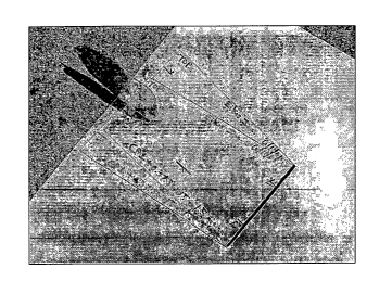
colorless as depicted in Fig. 12. This coating was formed by casting a
solution of POLYIMIDE-1 with 0.3% SWNTs @ 1.5 ~m final thickness.
CA 02442310 2003-09-26
WO 02/076724 PCT/US02/09140
It has a resistivity of 108 Ohms sq with transparency 96%T with haze of
0.6%.
This excellent coating demonstrates that by manipulating the
concentration and coating thickness excellent optical and electrical
5 properties can be obtained in the same film. For comparison, the same
sample was tested in our UV-Vis spectrometer at SOOnm. The glass
complicates the results since the ESD layer acts as an antireflective
coating to the glass and alters the reflective components contribution to the
transmission result. Nevertheless, this coating demonstrates the potential
10 for very high clarity ESD coatings.
Table 12 Transmission at SOOnm for thin 0.3%
POLYIMIDE-1 coating on glass
Gar.,'~'~~~''~, .~ ..~.~ ~y '~d,El!'!~5'q..'k.,.,~",,~
Sa~m~le ~~ W'~' ~y- ~
~D~es~cr~iption /o ~"500~~ J,Y
nor yv/ glass Resistor
~ subtracted ~~ ~y
in
Ohmsl$q.
~~
Ultrathin monolayer of
POLYIMIDE-1 with 0.3% 83.8 3E+8
SWnT 0.5 mil cast
Blank piece of glass 88.8 >10
To reduce optical absorbance in nanocomposite conductive films the
15 coating can be formed from a thin monolayer of high concentration
nanotubes. Several other techniques have also been demonstrated to
achieve the same high optical transparency while maintaining high
electrical conductivity in the film. Two of the most successful rely on the
same concept just shown, they are: 1) the use of bi-layers and 2) ultra thin
20 polymer wrapped nanotubes.
Bi-layer and Special ultra thin ESD Films.
CA 02442310 2003-09-26
WO 02/076724 PCT/US02/09140
36
A natural extension of the thin coating method for high optical clarity
coatings, is to form a bi-layer free standing film by cast the thin 1 ~m
layer first on glass and then over coating with the thicker, 25 um layer of
virgin resin. The resulting film has a conductive surface without
conductivity through the thickness. We made films from the TPO resin to
demonstrate the concept. The specifications for this film are provided in
Table 13.
Nanotube concentration was increased to almost 50% in the conductive
layer. This was done by modifying the nanotubes with a coating of
polyvinylpyrrolidone (PVP). This is also referred to as wrapping the
nanotubes with a helical layer of polymer. To accomplish this, SWNTs
were suspended in sodium dodecy sulfate and PVP. This solution was
then incubated at 50°C for 12 hours and then flocculated with IPA. The
solution is centrifuged and washed in water three times and then
suspended in water. The resulting nanotubes are water soluble and easily
sprayed or cast onto any surface. This solution was spray coated onto
virgin films to create a fine coating (<lum thick) that has ESD properties
and is very clear and colorless.
The resulting coating can be coated with a thin binder while still
remaining conductive or coated with a thicker layer to make free standing
films. Using this technique, coatings with a resistivity down to 100 Ohms
were generated.
Although only a few exemplary embodiments of the present invention
have been described in detail in this disclosure, those skilled in the art who
review this disclosure will readily appreciate that many modifications are
possible in the exemplary embodiments (such as variations in sizes,
structures, shapes and proportions of the various elements, values of
parameters, or use of materials) without materially departing from the
CA 02442310 2003-09-26
WO 02/076724 PCT/US02/09140
37
novel teachings and advantages of the invention. Accordingly, all such
modifications are intended to be included within the scope of the invention
as defined in the appended claims.
Other substitutions, modifications, changes and omissions may be made in
the design, operating conditions and arrangement of the preferred
embodiments without departing from the spirit of the invention as
expressed in the appended claims.
Additional advantages, features and modifications will readily occur to
those skilled in the art. Therefore, the invention in its broader aspects is
not limited to the specific details, and representative devices, shown and
described herein. Accordingly, various modifications may be made
without departing from the spirit or scope of the general inventive concept
as defined by the appended claims and their equivalents.
All references cited herein, including all U.S. and foreign patents and
patent applications, all priority documents, all publications, and all
citations to government and other information sources, are specifically and
entirely hereby incorporated herein by reference. It is intended that the
specification and examples be considered exemplary only, with the true
scope and spirit of the invention indicated by the following claims.
As used herein and in the following claims, articles such as "the", "a" and
"an" can connote the singular or plural.