Note: Descriptions are shown in the official language in which they were submitted.
CA 02442929 2009-08-18
= 1
METHOD OF FABRICATING AN OXIDE LAYER ON A SILICON CARBIDE
LAYER UTILIZING AN ANNEAL IN A HYDROGEN ENVIRONMENT
Statement of Government Interest
The present invention was made, at least in part, with support from United
States
Air Force Wright Labs contract number F33615-99-C-2914. The Government may
have
certain rights in this invention.
Field of the Invention
The present invention relates to the fabrication of semiconductor devices and
more
particularly, to the fabrication of oxide layers on silicon carbide (SiC).
Background of the Invention
Devices fabricated from silicon carbide are typically passivated with an oxide
layer, such as Si02, to protect the exposed SiC surfaces of the device and/or
for other
reasons. However, the interface between SiC and Si02 may be insufficient to
obtain a
high surface mobility of electrons. More specifically, the interface between
SiC and
CA 02442929 2009-08-18
2
Si02 conventionally exhibits a high density of interface states, which may
reduce surface
electron mobility.
Recently, annealing of a thermal oxide in a nitric oxide (NO) ambient has
shown
promise in a planar 4H-SiC MOSFET structure not requiring a p-well implant.
See M.
K. Das, L. A. Lipkin, J. W. Palmour, G. Y. Chung, J. R. Williams, K. McDonald,
and L.
C. Feldman, "High Mobility 4H-SiC Inversion Mode MOSFETs Using Thermally
Grown, NO Annealed Si02," IEEE Device Research Conference, Denver, CO, June 19-
21, 2000 and G. Y. Chung, C. C. Tin, J. R. Williams, K. McDonald, R. A.
Weller, S. T.
Pantelides, L. C. Feldman, M. K. Das, and J. W. Palmour, "Improved Inversion
Channel
Mobility for 4H-SiC MOSFETs Following High Temperature Anneals in Nitric
Oxide,"
IEEE Electron Device Letters accepted for publication. This anneal is shown to
significantly reduce the interface state density near the conduction band
edge. G. Y.
Chung, C. C. Tin, J. R. Williams, K. McDonald, M. Di Ventra, S. T. Pantelides,
L. C.
Feldman, and R. A. Weller, "Effect of nitric oxide annealing on the interface
trap
densities near the band edges in the 4H polytype of silicon carbide," Applied
Physics
Letters, Vol. 76, No. 13, pp. 1713-1715, March 2000. High electron mobility
(35-95
cm2/Vs) is obtained in the surface inversion layer due to the improved MOS
interface.
Unfortunately, NO is a health hazard having a National Fire Protection
Association (NFPA) health danger rating of 3, and the equipment in which post-
oxidation anneals are typically performed is open to the atmosphere of the
cleanroom.
They are often exhausted, but the danger of exceeding a safe level of NO
contamination
in the room is not negligible.
Growing the oxide in N20 is possible as described in J. P. Xu, P. T. Lai, C.
L.
Chan, B. Li, and Y. C. Cheng, "Improved Performance and Reliability of N20-
Grown
Oxynitride on 6H-SiC," IEEE Electron Device Letters, Vol. 21, No. 6, pp. 298-
300, June
2000. Xu et al. describe oxidizing SiC at 1100 C for 360 minutes in a pure
N20
ambient and annealing in N2 for 1 hour at 1100 C.
Post-growth nitridation of the oxide on 6H-SiC in N20 at a temperature of
1100 C has also been investigated by Lai et al. P. T. Lai, Supratic
Chakraborty, C. L.
Chan, and Y. C. Cheng, "Effects of nitridation and annealing on interface
properties
CA 02442929 2009-08-18
3
of thermally oxidized SiO2/SiC metal-oxide-semiconductor system," Applied
Physics
Letters, Vol. 76, No. 25, pp. 3744-3746, June 2000. However, Lai et al.
concluded
that such treatment deteriorates the interface quality which may be improved
with a
subsequent wet, or dry anneal in 02 which may repair the damage induced by
nitridation
in N20. Moreover, even with a subsequent 02 anneal, Lai et al. did not see any
significant reduction in interface state density as compared to the case
without nitridation
in N20.
In addition to NO and N20 growth and annealing, research has also been
conducted on post growth anneals in other environments. For example, Suzuki et
al.
investigated post oxidation annealing in hydrogen. Suzuki et al., "Effect of
Post-
oxidation-annealing in Hydrogen on Si02/4H-SiC Interface," Material Science
Forum,
Vols. 338-342, pp. 1073-1076, 2000. These researchers reported that flat-band
voltage
shift and interface state density could be improved by post oxidation
annealing in both
argon and hydrogen. In this research, 4H-SiC was oxidized in dry 02 at 1200
C. Post
oxidation annealing was then carried out in argon or hydrogen for 30 minutes
at 400,
700, 800 and 1000 C. Other researchers, however, have reported that post
oxidation
anneals in hydrogen provide no increased benefit over post oxidation anneals
in other
gases. Mrinal Das, "Fundamental Studies of the Silicon Carbide MOS Structure,"
Doctoral Thesis, Purdue University, submitted December, 1999.
Summary of the Invention
Embodiments of the present invention provide for fabricating a silicon carbide
structure by fabricating a nitrided oxide layer on a layer of silicon carbide
and
annealing the nitrided oxide layer in an environment containing hydrogen. Such
a
fabrication of the nitrided oxide layer may be provided by forming, annealing
or
forming and annealing the oxide layer in at least one of nitric oxide, nitrous
oxide
and/or an ambient containing a reactive nitrogen species. Alternatively, the
nitrided
oxide layer may be provided by fabricating an oxide layer and fabricating a
nitride
layer on the oxide layer so as to provide the nitrided oxide layer on which
the nitride
layer is fabricated. Such a formation of a nitride layer may both provide the
nitrided
oxide layer and hydrogenate the nitrided oxide layer as hydrogen may be a
byproduct
of the formation of the nitride layer. Furthermore, in such embodiments,
hydrogen
CA 02442929 2003-10-01
WO 02/084727 PCT/US02/11691
4
annealing the oxide layer may be provided substantially concurrently with the
step of
fabricating the nitride layer.
In particular embodiments of the present invention, the silicon carbide layer
comprises 4H polytype silicon carbide. The silicon carbide layer may be a
silicon
carbide layer on a non-silicon carbide substrate, a silicon carbide layer on a
silicon
carbide substrate and/or a portion of a silicon carbide substrate.
In further embodiments of the present invention, annealing the oxide layer is
provided by a subsequent processing step which heats the oxide layer to a
temperature
of greater than about 400 C in a hydrogen containing environment whether it
be a
part of a separate anneal step or other such processing step. In other
embodiments of
the present invention, the oxide layer is annealed at a temperature of greater
than
about 400 C in a hydrogen containing environment. The oxide layer may also be
annealed at a temperature of between about 400 C and about 1000 C in a
hydrogen
containing environment. In particular embodiments of the present invention,
the oxide
layer is annealed at a temperature of less than about 900 C in a hydrogen
containing
environment. Preferably, the oxide layer is annealed at a temperature of
between
about 400 C and about 800 C in a hydrogen containing environment.
Additionally,
the anneal may be carried out for a time of greater than about 2 minutes.
In still further embodiments of the present invention, processing steps
subsequent to the anneal in a hydrogen containing environment high temperature
processing steps are also carried out in a hydrogen containing environment.
In additional embodiments of the present invention, the hydrogen anneal is
preceded by forming metallization for a semiconductor device associated with
the
oxide layer. In such embodiments, the hydrogen anneal of the oxide layer can
be
provided by annealing the oxide layer at a temperature of less than about 900
C in a
hydrogen containing environment. In such embodiments, the annealing of the
oxide
layer may be a contact anneal. Additionally, a silicon carbide metal oxide
semiconductor device may be formed having the oxide layer as a gate oxide of
the
metal oxide semiconductor device.
In particular embodiments of the present invention, the nitrided oxide is
annealed in forming gas having about 4% hydrogen and about 96% inert gases.
In still further embodiments of the present invention, an oxide layer on a
silicon carbide layer is fabricated by nitriding the oxide layer on the
silicon carbide
layer with at least one of nitric oxide and nitrous oxide and annealing the
nitrided
CA 02442929 2009-08-18
oxide layer at a temperature of between about 400 C about 900 C in a
hydrogen
containing environment for at least about 2 minutes.
Accordingly, in one aspect of the present invention there is provided a method
of
a forming an insulator in a silicon carbide electronic device, comprising,
fabricating a
5 nitrided oxide layer on a layer of silicon carbide, and annealing the
nitrided oxide layer
in an environment containing at least one of H2 and NH3, wherein the step of
fabricating
a nitrided oxide layer comprises at least one of (a) forming the nitrided
oxide layer by
oxidizing the layer of silicon carbide in an atmosphere containing at least
one of nitric
oxide and nitrous oxide at a temperature of 1200 C or higher and (b)
annealing an
existing oxide layer in an atmosphere containing at least one of nitric oxide
and nitrous
oxide at a temperature of 1175 C or higher.
According to another aspect of the present invention there is provided a
method
of fabricating an oxide layer on a silicon carbide layer, comprising,
nitriding the oxide
layer on the silicon carbide layer in nitrous oxide at a temperature of at
least 1200 C,
and annealing the nitrided oxide layer at a temperature of between 400 C 900
C in an
environment containing at least one of H2 and NH3 for at least about 2
minutes.
Brief Description of the Drawings
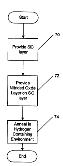
Figure 1A is a flowchart illustrating processing steps for hydrogen annealing
according to embodiments of the present invention;
Figure 1B is a flowchart illustrating the incorporation of additional
processing
steps with hydrogen annealing according to further embodiments of the present
invention;
Figure 2 is a schematic illustration of a furnace tube suitable for use in
embodiments of the present invention;
Figure 3 is a graph of DI I versus energy level from the conduction band for
various thermal oxidation, post-growth N20 anneals and N20 oxidation;
Figures 4A and 4B are graphs of interface state density for an oxide which has
been N20 annealed at 1300 C measured before and after anneal at 800 C in a
forming
gas of 4% hydrogen and 96% inert gases according to embodiments of the present
invention;
Figure 5 is a graph of capacitance versus voltage for capacitors having an
oxide which has been N20 annealed at 1300 C measured before and after anneal
at
800 C in a forming gas of 4% hydrogen and 96% inert gases according to
embodiments of the present invention; and
CA 02442929 2009-08-18
5a
Figure 6 is a graph of field effect mobility versus gate voltage for MOSFETs
having a gate oxide which has been N20 annealed at 1300 C measured before and
after
anneal at 800 C in a forming gas of 4% hydrogen and 96% inert gases according
to
embodiments of the present invention.
Detailed Description of the Invention
The present invention now will be described more fully hereinafter with
reference to the accompanying drawings, in which preferred embodiments of the
invention are shown. This invention may, however, be embodied in many
different
forms and should not be construed as limited to the embodiments set forth
herein;
rather, these embodiments are provided so that this disclosure will be
thorough and
complete, and will fully convey the scope of the invention to those skilled in
the art.
In the drawings, the thickness of layers and regions are exaggerated for
clarity. Like
CA 02442929 2009-08-18
6
numbers refer to like elements throughout. It will be understood that when an
element such as a layer, region or substrate is referred to as being "on"
another
element, it can be directly on the other element or intervening elements may
also be
present. In contrast, when an element is referred to as being "directly on"
another
element, there are no intervening elements present.
Embodiments of the present invention provide methods which may improve
the interface between an oxide layer and SiC in any device which includes such
an
interface. These methods are especially advantageous in the fabrication of
Metal-
Oxide-Semiconductor (MOS) devices created on SiC. Using embodiments of the
present invention, interface states with energy levels near the conduction
band of SiC
may be dramatically reduced. Reduction of such defects may be advantageous,
because these defects may limit a MOS device's effective surface channel
mobility.
Embodiments of the present invention will now be described with reference to
Figures 1A and 1B which are flow charts illustrating operations according to
particular
embodiments of the present invention. As illustrated in Figure 1A, embodiments
of
the present invention utilize an anneal of a nitrided oxide layer to further
reduce
interface state densities at the silicon carbide oxide boundary. As used
herein, the term
nitrided oxide layer refers to oxide layers formed or subsequently annealed
(as a
separate anneal step and/or as subsequent processing such as the deposition of
a nitride
or oxynitride layer) in the an atmosphere which yields chemically reactive
nitrogen
species, such as nitrogen precursors, including nitric oxide (NO) and/or
nitrous oxide
(N20), and/or as part of a processing step where a reactive nitrogen species
is a
byproduct, to thereby introducing nitrogen into the layer.
Turning to Figure 1A, a silicon carbide layer is provided (block 70). The SiC
layer may be an epitaxial layer and/or a substrate. A nitrided oxide layer is
provided
on the silicon carbide layer (block 72). The nitridation may be provided, as
described
herein, by growth and/or anneal in an N20 and/or NO environment. Similarly,
nitridation of the oxide layer may be provided by processing steps for
deposition of a
nitride layer on the oxide layer, for example, in an oxide-nitride (ON) or
oxide-nitride-
oxide (ONO) structure. ONO and ON structures are described in commonly
assigned United States Patent No. 6,246,076. For embodiments where the
nitrided
oxide layer is provided by an anneal, the oxide layer may be formed by
deposition,
such as Low Pressure Chemical Vapor Deposition (LPCVD), thermally grown
CA 02442929 2009-08-18
7
through a thermal oxidation process and/or formed using other techniques.
Preferably,
the oxide layer is formed utilizing a wet reoxidation process as described in
United
States Patent No.5,972,80 1.
The nitrided oxide layer is annealed in a hydrogen containing environment
(block 74). Such an anneal may be a separate processing step or may be part of
a
subsequent deposition or other such process, for example, the deposition of a
nitride
layer on an oxide layer in a wet environment may provide both the nitridation
and
anneal. The anneal is preferably carried out at a temperature of greater than
about 400
C and less than about 1000 C. Preferably, the anneal is carried out at a
temperature
of from about 400 C to about 800 C. The anneal is preferably carried out for
about 2
or more minutes.
The anneal in a hydrogen containing environment may be carried out
immediately after nitridation or intervening steps may be performed before the
anneal.
Thus, as illustrated in Figure 1B, the anneal may be provided as a subsequent
processing step which provides a contact anneal. As seen in Figure 1B, a
nitrided
oxide layer is provided on a SiC layer (blocks 80 and 82). Further device
fabrication
may then be performed to provide a silicon carbide semiconductor device (block
84).
As part of or separate from the device fabrication, contact metallization is
fabricated
for the device (block 86). The contact metallization is then subjected to a
contact
anneal in a hydrogen containing environment (block 88), preferably at a
temperature
of greater than about 400 C and less than about 900 C. Thus, the contact
anneal
provides at least part of the anneal of the nitrided oxide layer in a hydrogen
containing
environment. Subsequent high temperature processing steps are then also
carried out
in a hydrogen containing environment (block 90).
For example, in a silicon carbide metal oxide semiconductor device, the
anneal may be provided subsequent to metallization of the device by performing
a
contact anneal in a hydrogen containing environment at a temperature of less
than
about 900 C. Thus, for example, the oxide layer may provide a gate oxide of a
metal
oxide semiconductor field effect transistor (MOSFET). The contact anneal may
anneal the contacts of the device as well as provide the anneal of the
nitrided oxide.
Whenever in the fabrication process the anneal of the nitrided oxide layer
takes place,
it may be preferred that subsequent high temperature (i.e. processing at
temperatures
CA 02442929 2003-10-01
WO 02/084727 PCT/US02/11691
8
greater than about 400 C) processing be conducted in a hydrogen containing
environment.
As used herein, the term hydrogen containing environment refers to hydrogen
and/or a hydrogen precursor either alone or in combination with other gases.
For
example, a forming gas of 4% hydrogen and 96% argon may be utilized for the
hydrogen anneal. Similarly, the hydrogen may be provided by a hydrogen
precursor,
such as NH3 and/or may be a byproduct of a processing step. Thus, the present
invention should not be construed as limited to pure hydrogen environments but
includes hydrogen and/or hydrogen precursors as a constituent gas with other
gases as
well.
Figure 2 is an illustration of a furnace tube suitable for use in particular
embodiments of the present invention to provide the nitrided oxide layer. As
seen in
Figure 2, the furnace tube 10 has a plurality of wafers 12 of SiC either with
an oxide
layer, such as Si02, formed thereon or on which an oxide layer is to be
formed.
Preferably, the SiC wafer is 4H-SiC. The wafers 12 are placed on a carrier 14
such
that the wafers will, typically have a fixed position in the furnace tube 10.
The carrier
14 is positioned so that the wafers are a distance L1+L2 from an inlet of the
furnace
tube 10 and extend for a distance L3 within the furnace tube 10. Input gases
16,
which may include N20 and/or NO, are passed into the furnace tube 10 and are
heated
as they traverse the distance L1 based on a predetermined temperature profile
so as to
provide the heated gases 18. The heated gases 18 may be maintained at
temperatures
based on the predetermined temperature profile and traverse the distance L2 to
reach
the first of the wafers 12. The heated gases 18 continue to pass through the
furnace
tube 10 until they leave the furnace tube 10 through an outlet port as exhaust
gases 20.
Thus, the heated gases 18 traverse the distance U. The heated gases 18 are
preferably maintained at a substantially constant temperature for the
distances L2 and
L3, however, as will be appreciated by those of skill in the art in light of
the present
disclosure, various temperature profiles may also be utilized. Such profiles
may
include variations in temperature over time and/or distance. However, in
embodiments where the nitrided oxide layer is provided by an N20 anneal and/or
oxidation, the predetermined temperature profile should include either an
anneal
temperature of greater than about 1100 C or an oxidation temperature of at
least
about 1200 C.
CA 02442929 2003-10-01
WO 02/084727 PCT/US02/11691
9
As is seen in Figure 2, the heated gases 18 may reach a temperature at which
the N20 begins to break down into its constituents at the end of the L1
distance. This
distance may depend on the physical characteristics of the furnace tube 10,
the
predetermined temperature profile and the flow rate profile. The heated gases
18 also
traverse the distance L2 before reaching the wafers 12. The amount of time
that it
takes the heated gases to traverse the distance L2 is referred to herein as an
"initial
residence time." Preferably, the heated gasses are maintained at a
substantially
constant temperature corresponding to an anneal temperature of greater than
about
1100 C or an oxidation temperature of at least about 1200 C for the initial
residence
time. However, as will be appreciated by those of skill in the art, differing
heating
profiles could be utilized which increase or decrease the initial residence
time. It
may be preferred, however, that the heating profile be rapid such that the
initial
residence time is substantially the same as the time that the heated gases 18
are
maintained at an anneal temperature of greater than about 1100 C or an
oxidation
temperature of at least about 1200 C before traversing the L3 distance.
The total amount of time that it takes the heated gases 18 to traverse the
distance L2+L3 is referred to herein as the "total residence time." As will be
appreciated by those of skill in the art in light of the present disclosure,
these
residence times depend on the velocity of the heated gases 18 through the
furnace
tube 10 which may be determined based on the flow rates of the heated gases 18
and
the cross-sectional area of the furnace tube 10. Such velocities may be
average
velocities, for example, if turbulent flow is achieved, or may be actual
velocities, for
example, in laminar flow systems. Thus, the term velocity is used herein to
refer to
both average and actual velocities.
As discussed above, the nitrided oxide layer may be provided by, among other
ways, growth and/or anneal in an NO and/or an N20 environment. NO growth
and/or
annealing as described above may be utilized alone or in combination with N20
growth and/or annealing. If the nitrided oxide layer if provided by growth
and/or
annealing in an N20 environment, it is preferred that such growth and/or
annealing be
carried out at a predetermined temperature and a predetermined flow rate as
described
herein.
For N20 annealing, preferably, the oxide is annealed using a predetermined
temperature profile which includes an anneal temperature of greater than about
1100
CA 02442929 2003-10-01
WO 02/084727 PCT/US02/11691
C in a chamber in which N20 is supplied at a flow rate profile within
predetermined
flow rate limits. Preferably, the temperature of the anneal is about 1175 C
or higher
and more preferably, about 1200 C may be utilized. The flow rate limits of
N20
may be selected based on the particular equipment in which the process is
used.
5 However, in particular embodiments the flow rate limits of N20 may be as low
as
about 2 Standard Liters per Minute (SLM) or as high as about 8 SLM. In further
embodiments, flow rate limits of from about 3 to about 5 SLM may be preferred.
For
particular furnaces as illustrated in Figure 2, gas velocities as low as about
0.37
cm/sec or as high as about 1.46 cm/sec or velocities of from about 0.55 cm/s
to about
10 0.95 cm/s may be suitable. In particular, for an L2 distance of about 12
inches (about
30.48 cm) and an L3 distance of about 18 inches (about 45.72 cm), such
velocities
result in an initial residence time of from about 11 seconds to about 45
seconds and a
total residence of from about 28 seconds to about 112 seconds. In particular
preferred
embodiments, the initial residence time is from about 16 seconds to about 31
seconds
and a total residence time of from about 41 to about 73 seconds. The N20
and/or NO
anneal may be carried out for about 3 hours, however, anneals of from about 30
minutes to about 6 hours may also be utilized although longer times may also
be
utilized.
For N2O growth, preferably the SiC wafers 12 are oxidized using a
predetermined temperature profile which includes an oxidation temperature of
greater
than about 1200 C in a chamber in which N20 is supplied at a flow rate
profile
within predetermined flow rate limits. Preferably, the temperature of the
oxidation is
about 1300 C. The flow rate limits of N20 may be selected based on the
particular
equipment in which the process is used. However, in particular embodiments,
the
flow rate limits of N20 may be as low as about 2 Standard Liters per Minute
(SLM)
or as high as about 6 SLM or higher. In further embodiments, flow rate limits
of from
about 3.5 SLM to about 4 SLM may be preferred. Thus, for a particular
apparatus,
gas velocities as low as about 0.37 cm/sec or as high as about 1.11 cm/sec may
be
utilized, while velocities of from about 0.65 cm/s to about 0.74 cm/s may be
preferred. In particular, for an L2 distance of about 12 inches (about 30.48
cm) and
an L3 distance of about 18 inches (about 45.72 cm), such velocities result in
an initial
residence time of from about 11 seconds to about 33 seconds and a total
residence
time of from about 28 seconds to about 84 seconds. In particular preferred
CA 02442929 2003-10-01
WO 02/084727 PCT/US02/11691
11
embodiments, the initial residence time is from about 19 second to about 22
seconds
and the total residence time is from about 49 to about 56 seconds. The N20
oxidation
may be carried out for an amount of time dependent on the desired thickness of
the
oxide layer. For example, oxidation times of about 3 hours or greater may be
utilized.
As used herein, N20 refers to pure N20 or N20 in combination with other
oxidizing
agents, such as steam, 02, and/or inert gases.
Oxidation in an NO and/or N2O environment and/or anneals in an NO and/or
N20 environment may be followed by an optional anneal in inert gas or gases,
such as
argon and/or N2 or combinations thereof with other gases. Such an anneal may
be
carried out for about 1 hour, however, anneals of up to about 3 hours or
longer may
also be utilized.
Figures 3 through 6 illustrate results which may be obtained utilizing
embodiments of the present invention. Figure 3 illustrates results which were
obtained for N20 growth and N2O annealing without subsequent annealing in a
hydrogen containing environment. Figures 4A, 4B, 5 and 6 illustrate results
obtained
with a hydrogen anneal of a nitrided oxide layer.
As shown in Figure 3, the solid line represents a thermally grown oxide
without nitridation. At lower temperatures (1100 C), exposing an existing
oxide to
N20 increases the interface state density, as shown by comparing the heavy
solid line
representing a thermal oxide to the data for the same thermal oxide exposed to
an
1100 C N20 anneal. At 1200 C, the thermal oxide is significantly improved with
the
N2O anneal. Thermal oxides processed in a wet ambient may be further improved
by
the 1200 C N2O anneal, as seen by comparing the solid circle to the open
circle data.
Further improved results were obtained using a 1300 C N2O anneal process (the
DRY-1300 line) and the 1300 C N20 growth process (the 1300 grown line). At
this
temperature, the oxidation of SiC is significant. So, in addition to annealing
existing
oxides in N20, some oxides were grown in the N20 ambient (500 A was grown in 3
hours). Growing the oxide in N2O may save about 9 hours of processing time
over
annealing an existing oxide in N2O, by eliminating the oxidation step. As is
seen in
Figure 3 by comparing the Dry-1300 line to the 1300 grown line, substantially
the
same results were obtained regardless of whether the oxide was grown prior to
N2O
processing or grown in N20.
CA 02442929 2003-10-01
WO 02/084727 PCT/US02/11691
12
Figures 4A and 4B are graphs of interface state density for an oxide which has
been N20 annealed at 1300 C measured before and after anneal at 800 C in a
forming gas of 4% hydrogen and 96% inert gases. As is illustrated in Figure
4A, line
180 illustrates the interface trap density for the oxide before the anneal and
line 182
after the anneal. In Figure 4B, line 184 illustrates the interface trap
density for the
oxide before the anneal and line 186 after the anneal. Lines 180 and 184 may
represent the lowest reported values for DIT on the 4H-SiC MOS interface. The
4%
hydrogen present in the forming gas further improves this result on both the
upper
(Figure 4B) and lower (Figure 4A) halves of the bandgap.
Figure 5 is a graph of capacitance versus voltage for capacitors having an
oxide which has been N20 annealed at 1300 C measured before and after anneal
at
800 C in a forming gas of 4% hydrogen and 96% inert gases. In Figure 5, line
190
illustrates the capacitance for the oxide before the anneal and line 192 after
the
anneal. As is seen in Figure 5, the forming gas anneal reduces the flatband
voltage
by 4.5 Volts, which corresponds to a 1.7E12 cm -2 reduction in effective oxide
charge.
Figure 6 is a graph of field effect mobility versus gate voltage for MOSFETs
having a gate oxide which has been N20 annealed at 1300 C measured before and
after anneal at 800 C in a forming gas of 4% hydrogen and 96% inert gases. In
Figure 6, line 200 illustrates field effect mobility for MOSFETs with a
nitrided gate
oxide before the anneal and line 202 after the anneal. As is seen in Figure 6,
inversion channel mobility increases by almost 20% and the threshold voltage
is
reduced by 2 V.
In the drawings and specification, there have been disclosed typical preferred
embodiments of the invention and, although specific terms are employed, they
are
used in a generic and descriptive sense only and not for purposes of
limitation, the
scope of the invention being set forth in the following claims.