Note: Descriptions are shown in the official language in which they were submitted.
CA 02442932 2003-10-03
WO 02/082122 PCT/US02/10375
SCINTILLATION DETECTOR, SYSTEM AND METHOD
PROVIDING ENERGY & POSITION INFORMATION
The invention described herein relates generally to scintillation detectors
sensitive
s to ionizing radiation, to a method for performing radiation-based
measurements, and also
to methods of manufacture for such scintillation detectors. The scintillation
detectors and
methods are particularly useful for imaging in nuclear medicine applications,
but may have
use in other applications where the radiation energy passing into the
scintillator or the
position of interaction of the radiation with the scintillator are of
interest.
~o Scintillation detectors have been employed in medical imaging applications
for
some years and are embodied in devices called "gamma cameras" and also called
"Anger"
cameras after the developer, H.O. Anger. Typically, these cameras use
scintillation crystals
of sodium iodide doped with thallium as detectors for detecting gamma rays
from
radiopharmaceuticals used in nuclear medicine studies. The crystals are
typically round or
rectangular plates with their largest dimensions from 12 to 30" in diameter or
diagonal.
These sodium iodide crystal detectors have a typical thickness of 3/8" to %2'
(0.9 cm to 1.3
cm), sufficient for highly efficient detection of gamma rays emitted from the
isotope Tc-
199m, which is included in many radiopharmaceuticals and emits gamma radiation
with an
energy of 140 keV. For other isotopes, other crystal thicknesses may be
appropriate.
2o A typical gamma camera detector assembly 20 is diagrammatically illustrated
in
Figs. 1 a and 1 b. Radiation quanta 21 incident on the assembly 20 via a
collimator 22
interact with the crystal 24 to produce an amount of scintillation light
uniquely and nearly
linearly related to the amount of energy transferred to the crystal by the
radiation. The
amount of energy in the incident radiation quanta may be one parameter of
interest to the
2s user and, as a result, precise determination of the energy deposited in the
crystal is of
considerable interest. In particular, the user is interested in knowing
whether the incident
quanta has the full energy of the emitting isotope or whether it has somewhat
less energy,
since energy loss can result from scatter in the patient or the detector.
Scattered radiation
degrades the quality of the image. The energy information is represented by
the amount of
so light produced by the scintillation crystal.
As is also shown in Figs. 1 a and 1 b, the typical detector assembly 20
includes an
optical system for collecting the light produced in the scintillation crystal
24 and a light
conversion system for electronically sensing the light collected. There are
two main
components in the optical system. One is an optical window 26, typically
glass, which may
35 be bonded to one face of the crystal 24 with a transparent optical adhesive
27. The other
is a reflector 28 which typically covers the remaining surfaces of the
crystal. Figs. 1a and
-1-
CA 02442932 2003-10-03
WO 02/082122 PCT/US02/10375
1 b also show an array of light sensors 30, typically photomultiplier tubes
(PMT's), which
are used to sense the light signal and convert it into an electrical signal
pulse uniquely and
typically nearly linearly related to the light incident on the Light sensor.
Usually an optical
coupling material 32 such as an optical coupling grease or potting compound is
used to
s optically couple the PMT's to the optical window.
The package for the crystal is a moisture-impermeable housing 34 covering all
sides of the crystal 24 except the portion covered by the optical window 26.
This housing
34 is typically made of aluminum and is typically bonded to the edges of the
glass optical
window 26 ~rrith moisture-resistant adhesive 35, such as an epoxy, to provide
a hermitic
~o seal in the case of hygroscopic crystals such as Thallium-doped sodium
iodide. The
housing serves to prevent entrance of moisture while allowing entrance of the
gamma
radiation of interest. Amplification and signal processing electronics 37 are
used to
analyze and display the electrical information.
The user's desire for accurate energy information may be best met with an
optical
s system that directs or redirects all the original light toward and into the
light sensors, so
that all light produced is collected and converted faithfully into electrical
signals. Loss of
light without sensing reduces the energy information available. The higher the
light
production and light collection efficiency, the better the energy information
quality, which is
often expressed as the "energy resolution" or "spectrum peak full width at
half maximum".
2o Reflection is important for maximizing light collection and energy
information: As
depicted in Fig. 1a, light from a radiation interaction (event) 40 that is
originally directed
away from the light sensors encounters the crystal surface and some is
reflected by the
index of refraction mismatch between the crystal and the surrounding air. This
is
represented by the light path "A" in the Fig. 1 a. Some of the light may also
pass through
2s the crystal surface and encounter the reflector 28, as is represented by
the light path "B" in
the Fig.1 a. The reflector redirects this light so that it also has the
possibility of being
collected by the PMT's.
There are also other, less helpful reflections in the optical system. Light
reaching
the boundary between the crystal 24 (index of refraction about 1.8 for sodium
iodide) and
so the optical coupling compound 27 (index of refraction typically 1.5 or
less) is also reflected
by the index of refraction mismatch between the crystal and optical coupling
compound 27
as is depicted by the light path "C" in Fig. 1 a. These reflections direct
light away from the
PMT's. Multiple reflections of the favorable and unfavorable types may occur
before light is
collected and sensed, or finally lost. In a typical system, the outputs of the
PMT's are
-2-
CA 02442932 2003-10-03
WO 02/082122 PCT/US02/10375
adjusted to be normalized, so that their sum is directly representative of the
total light
collection and the desired energy information.
The location of the radiation interaction usually is also of interest to the
user. For
this reason an array of light sensors 30 is used to sense the light, rather
than a single
s position-insensitive light sensor. With proper design the light from a
radiation interaction
40 in the crystal is distributed among several PMT's. Prior determination of
the distribution
functions for light among the several PMT's as a function of position allows
later electronic
and software determination of the location of a gamma ray interaction in the
crystal. What
is important for position determination is the spreading of the light, meaning
its distribution
~o in relation to the light sensor network. Roughly speaking, if light were to
impinge on only a
single position-insensitive Light sensor, no position information could be
extracted. Also, if
the light spreads among too many PMT's, the signal amplitude in each will be
low and
therefore too easily influenced by electronic noise. A preferred situation is
to distribute the
°light among a relatively small number of PMT's. As with energy
determination, precise
location of an event is aided if more light is collected, but as mentioned,
the distribution is
also needed for position determination. The multiple reflections mentioned
earlier tend to
spread the light collection area for determining event position beyond the
preferred range
only encompassing a few PMT's.
In Anger's method, position signals are derived from a network of weighting
2o impedances related to a Light sensor hexagonal array and yield event
positions as X and Y
signals uniquely related to the X and Y Cartesian coordinate location of the
radiation
interaction. The sum of signals from all PMT's provides the desired energy
signal.
Combined with a radiation collimator and suitable electronics, such a system
provides
images of a patient's radio-pharmaceutical uptake for nuclear medical imaging.
2s The optical window 26 shown in Fig. 1 a heretofore has served multiple
functions.
First, it transmits light from the scintillator 24 to the PMT's. Second, it
may provide a
hermetic barrier protecting a hygroscopic sodium iodide crystal from attack by
moisture.
Third, it may provide mechanical support for the crystal and light sensors.
Fourth, it may
provide a controlled spacing between the crystal and PMT's which allows a
proper spread
so of light among the PMT's and provides an optimization of position and
energy analysis
compatible with other elements of the imaging system. The adjustment of light
spreading
can also be accomplished with an additional thickness of transparent light
pipe or light
guide material inserted between and optically coupled to the optical window
and PMT's.
To use the position-sensitive method developed by Anger, the crystal and
optical
ss window are optically continuous slabs essentially free of light scattering
defects, so that
-3-
CA 02442932 2003-10-03
WO 02/082122 PCT/US02/10375
light propagates directly or by reflection in a predictable way with
repeatable division
among the PMT's. Significant defects in the crystal or the glass will cast
shadows or
interrupt or alter the transport of light and thereby alter the quality of, or
introduce image
artifacts into, the resulting images. Part of the art of successfully
fabricating gamma
s camera radiation detectors lies in the production of high quality, large,
essentially
monocrystalline sodium iodide crystal plates and the fabrication of similar
size pieces of
high optical quality glass.
Collection of substantially all light requires highly efficient reflectors. As
a matter of
practice, crystal surfaces and reflectors arE hrpically chosen for diffuse
reflective
~o characteristics, rather than specular ones. Specular reflectors tend to
transport light to the
edges of the crystal, while diffuse reflectors tend to provide a more
favorable confined,
compact light distribution which retains the light in the area of interest to
permit position
sensing with a relatively small number of PMT's.
Gamma camera technology has evolved since Anger's developments so that the
15 determination of the position information may be done by techniques
different from an X-Y
impedance network, or ladder approach. Such alternative techniques include
direct signal
digitization and computer processing, nonlinear signal elements, and so forth.
Essentially,
though, these methods still rely on the collection of light from a large,
optically
homogeneous crystal in which light is distributed among a number of light
sensors, so that
2o the essential feature of the large gamma camera plate is to produce an
amount of light
proportional to the energy absorbed and to distribute the light reproducibly
among an array
of light sensors or upon a position-sensitive light sensor composed of light
sensor
elements. Design parameters such as the optical window thickness, the diffuse
nature of
the reflectors, or the degree of reflection, or all of these have an impact on
tuning and
25 optimizing the performance of the gamma camera crystal assembly in relation
to the full
camera sensing and computation system.
The description above of Anger's method and others has concentrated on planar
imaging. There is a derivative technique wherein the camera detector, or
several such
detectors, are moved to several positions, images acquired, and the results
processed to
so produce tomographic images of the radiation distribution in the patient.
This is referred to
as "Single Photon Emission Computed Tomography", or "SPELT" imaging. Both
SPELT
and planar imaging can be affected by absorption of the primary emission in
the patient.
Correction for this attenuation has led to methods for measurement and
calculation of
attenuation correction factors. Some of these methods involve the transmission
of
CA 02442932 2003-10-03
WO 02/082122 PCT/US02/10375
radiation through the patient from sources in known locations, a technique
which
sometimes results in high count rates at the detector.
Gamma camera detector pairs or arrays have also been applied to Positron
Emission Tomography, "PET" imaging, a nuclear medicine technique based on
s coincidence detection and positioning of positron annihilation radiation
without collimators.
This method of imaging operates at high count rates because there are no
collimators and
uses 511 keV radiation, the detection of which is enhanced by use of crystals
thicker than
those typically found in conventional gamma cameras.
Typical existing gamma camera detector assemblies like those described above
~o have the disadvantage that their effective use requires large, highly
transparent crystals
and associated glass window pieces with a high degree of optical perfection
over large
areas. They must have a high degree of freedom from bubbles, inclusions, or
other defects
which absorb light or alter its distribution.
These gamma camera detectors also have the disadvantage that all the PMT's are
~s optically connected to the entire crystal, so that radiation events
anywhere on the face of
the crystal activate large areas of the sensing and electronics analysis
system. This
means that the analysis system must accommodate count rates produced by the
entire
crystal or large portions of it. Work with transmission attenuation correction
and PET
studies on gamma cameras have increased the need for high rate counting. This
rate
20 limitation can be overcome partially by choosing to involve fewer PMT's in
each event
processing step, such as is described in U.S. Patent No. 5,576,547. While
involving fewer
PMT's improves rate capability, other properties may suffer. Too few PMT's
leads to light
transmission beyond the sensing area in use being lost for position or energy
determination purposes, or both. However, an alternative technique allowing
for high rates
25 is available. It involves essentially dividing the crystal into individual
pieces, or pixels, and
sensing position by noting which pixel is struck. This technique has count
rate advantages,
but also has cost disadvantages in that many more PMT's are required to
achieve the
same spatial resolution as is available from a conventional gamma camera.
The present gamma cameras cannot provide position information toward their
so edges because beyond about the middle of the last edge PMT in the sensing
array,
position information from properly located additional tubes is not available.
This leads to a
useful field of view which is smaller than the size of the crystal and
consequently effectively
to an edge region which is "dead". To partially mitigate this effect, the
optical window and
edge PMT's may extend beyond the edge of the crystal by a signification
fraction of the
35 PMT radius. However, such a glass extension or overhang precludes bringing
the edge of
-5-
CA 02442932 2003-10-03
WO 02/082122 PCT/US02/10375
the detector crystal close to the patient, an effect which also increases the
"dead" area of
the gamma camera head.
The gamma camera crystal and glass are typically flat, but can be shaped by
bending in one or more dimensions if necessary. While such shaping is
possible, the glass
s and crystal do not lend themselves easily to forming shapes which conform to
the body
and not at all to shapes which can be changed after fabrication. Annular
assemblies can
also be produced, but they have the disadvantage that thermal expansion
mismatches
between the Nal crystal and glass window tend to stress and break the optical
coupling
between the window and crystal as a result of changes in temperature.
1o Another shortcoming of the conventional gamma camera is that the light
sensitive
area of the PMT light sensor, the cathode, does not typically cover the entire
glass surface
of the optical window. For example, if the PMT's are round, there are
naturally spaces
between PMT's which are not covered with cathode material. The use of closely
packed
arrays of square or hexagonal PMT's partly corrects this problem, but while
the spaces
~s between cathodes are reduced in area, they still exist at the glass walls
of the PMT's where
no cathode material is present. Square and hexagonal tubes also typically have
the
disadvantage of higher cost because of their more complex shape and may
sometimes
have poorer performance due to electron collection problems arising from that
shape.
As has been seen, the need for position information requires that light be
2o distributed among PMT's rather than being directed only to the nearest non-
position
sensing PMT. This distribution requirement and the detector construction
details both
cause light to propagate beyond the PMT's best able to determine an event's
position and
in some cases cause the light to escape or be absorbed, thereby being lost to
the energy
signal. In other words, the requirement for light distribution and position
determination
2s inherently causes light to be lost, which in turn deteriorates position
determination and
energy signals.
The arrangement of the camera crystal with a contiguous optical window
introduces
four optical boundaries into the optical system, one between the crystal and
coupling
compound, another between the compound to the window, a third between the
optical
so window to another layer of coupling compound, and finally in the joining of
the final
coupling compound layer to the PMT. If there is any mismatch in the index of
refraction of
these layers, light is reflected and tends to be less useful for position
determination or may
be lost entirely.
-6-
CA 02442932 2003-10-03
WO 02/082122 PCT/US02/10375
From the above discussion, it can be concluded that there is a need for an
improved detector which reduces or eliminates one or more of the undesirable
effects
present in existing designs.
In accordance with the present invention, a novel radiation detector, in
particular a
gamma camera, is constructed and operated in such a fashion that only a
predetermined
number of light sensors (such as PMT's) adjoining each other in a cluster are
used to
generate a signal with amplitude and event position information. The novel
camera may
also use an array of individual scintillation elements (crystals) in place of
a single crystal,
with certain advantages obtained thereby. The invention also provides other
features that
~o are applicable to the foregoing detector and also to other types of
scintillation devices as
well.
According to one aspect of the invention, a scintillation detector comprises a
scintillator, a plurality of light sensors optically coupled to the
scintillator for producing light
sensor signals upon occurrence of a scintillation event in the scintillator
that produces light
~s sensed by the light sensors, and a processor for selecting a group of three
mutually-
adjoining light sensors having the highest amplitude light sensor signals
amongst the
plurality of light sensors for a particular radiation event, and for
determining the relative
position of the radiation event from the light sensor signals of the selected
group of light
sensors.
2o In a preferred embodiment, the plurality of light sensors are each equally
spaced
from mutually-adjoining light sensors, and the scintillator may comprise an
array of
triangular scintillator segments partially or completely optically isolated
from one another.
In one arrangement, each light sensor views three mutually contiguous
scintillator
segments, whereas in another arrangement each scintillator segment is viewed
by a
zs respective group of three mutually contiguous light sensors dedicated to
the respective
scintillator segment. Each segment may be formed by a respective discrete
scintillation
crystal, and a reflective bonding material may be interposed between
contiguous sides of
the scintillator segments to join the discrete segments to one another. The
segments may
also have tapered sides for positioning in a nonplanar arrangement, and the
discrete
so scintillation crystals may be mounted on a flexible substrate. In another
arrangement, a
scintillation crystal may have formed in a surface thereof a plurality of
slits separating
adjacent portions of the crystal, with each portion forming a respective one
of the
scintillation segments.
According to another aspect of the invention, there is provided a method of
ss obtaining event position information in a scintillation detector having a
scintillator and a
_7_
CA 02442932 2003-10-03
WO 02/082122 PCT/US02/10375
plurality of light sensors optically coupled to the scintillator for producing
light sensor
signals upon occurrence of a scintillation event in the scintillator that
produces light sensed
by the light sensors. The method comprises the steps of (a) selecting a group
of three
mutually-adjoining light sensors having the highest amplitude light sensor
signals amongst
s the plurality of light sensors for a particular radiation event; and (b)
determining the relative
position of the radiation event from the light sensor signals of the selected
group of light
sensors.
The invention also provides a scintillator and detector assembly comprising a
scintillator, and a plurality of light sensors optically coupled to the
scintillator for producing
~o light sensor signals upon occurrence of a scintillation event in the
scintillator that produces
light sensed by the light sensors, wherein the scintillator comprises an array
of triangular
scintillator segments partially or completely optically isolated from one
another.
According to a further aspect of the invention, a scintillation device
comprises a
housing, a scintillation crystal contained within the housing, and an optical
window closing
~s an open end of the housing, wherein a reflector is sandwiched between the
optical window
and the scintillation crystal, and the reflector defines an array of apertures
through which
scintillation light can pass from the scintillation crystal to and through the
optical window for
sensing by a plurality of light sensors optically coupled to the optical
window in an array
corresponding to the array of apertures in the reflector. This arrangement may
have
2o general application to scintillation devices of various types. In a
preferred embodiment, the
plurality of light sensors may be optically coupled to the optical window in
an array
corresponding to the array of apertures in the reflector, and the reflector
may include a
white polyester film.
According to yet another aspect of the invention, a scintillation device
comprises a
25 housing, a scintillation crystal contained within the housing, an array of
light sensors
optically coupled to the scintillation crystal, each light sensor having a
light sensitive
region, and a reflective film located between the scintillation crystal and
light sensors and
surrounding the light sensitive regions of the light sensors.
According to still another and more general aspect of the invention, a
scintillation
so device comprises a scintillator and a reflector disposed at a surface of
the scintillator for
reflecting scintillation light, wherein the reflector is made from a white
polyester reflective
material. Such a material has been found not to exhibit a significant loss of
reflectivity
when exposed to optical coupling and potting compounds which heretofore
significantly
degraded reflector performance.
_g_
CA 02442932 2003-10-03
WO 02/082122 PCT/US02/10375
The foregoing and other features of the invention are hereinafter fully
described and
particularly pointed out in the claims, the following description and annexed
drawings
setting forth in detail certain illustrative embodiments of the invention,
these embodiments
being indicative, however, of but a few of the various ways in which the
principles of the
s invention may be employed.
Fig. 1 a is a schematic sectional representation of a typical prior art gamma
camera
apparatus showing the relative positions of the PMT's, the gamma camera plate
assembly,
the radiation collimator, and the radiation source.
Fig. 1 b is a schematic top plan view of a fragment of the structure of Fig. 1
showing
~o a cluster of PMT's and the relative position of a scintillation event.
Fig. 2a is a schematic top plan view of the PMT's of a gamma camera apparatus
in
accordance with one embodiment of the invention which respond to the
scintillation event.
Fig. 2b is a graphical illustration of triangular math according to the
present
invention.
~s Fig. 2c is a schematic top plan view similar to Fig. 2a and showing
radiation events
at the center of a PMT and halfway between two PMTs.
Fig. 2d is a graph showing a typical normalized light response of a typical
light
sensor.
Fig. 3a is a schematic top plan view of the apparatus of Fig. 2a, together
with a
2o crystal which is an array of triangular crystal elements fitted together in
registry with an
array of PMT's so that each crystal element is associated with three PMT's.
Fig. 3b is a schematic top plan view of the apparatus of Fig. 2a, together
with a
crystal which is an array of larger triangular crystal elements than those of
Fig. 3a fitted
together in registry with an array of PMT's so that each crystal element is
associated with
25 three PMT's which are not associated with any other crystal elements.
Fig. 3c is a schematic top plan view of an edge fragment of the apparatus of
Fig.
3a, provided with two smaller PMT's associated with each crystal element in
order to
compensate for edge effects in the signal.
Fig. 3d is a schematic sectional view of the apparatus of Fig. 3a along the
line A-A
so in accordance with a further embodiment of the invention in which the
crystal is a larger
piece which is grooved to form triangular elements which are partially
optically isolated
from each other.
Fig. 3e is a schematic sectional view of the apparatus of Fig. 3a along the
line A-A
in accordance in which the triangular crystal elements are separate pieces
entirely optically
ss isolated from each other.
_g_
CA 02442932 2003-10-03
WO 02/082122 PCT/US02/10375
Fig. 4 is a schematic side, sectional view of a gamma camera plate assembly in
accordance with a preferred embodiment of the present invention having a thin
window
between the crystal and the PMT's for improving resolution.
Fig. 5a is a schematic top plan view of a gamma camera plate assembly in
s accordance with a preferred embodiment of the invention including a
reflector element for
gathering light which otherwise would pass or be absorbed outside the
photosensitive
areas of the PMT's.
Fig. 5b is a schematic side, sectional view of the assembly of Fig. 5a with
the
reflector element adjacent the perimeters of the PMT face plates immediately
surrounding
~o the photocathode sensitive areas.
Fig. 5c is a schematic side sectional view of the assembly of Fig. 5a with the
reflector element between the crystal and the window.
Aside from the differences described below, a detector system and method
(particularly a gamma camera and its method of operation) according to the
several below
~s described embodiments of the invention may be the same as the above-
described prior art
detector system shown in Figs. 1 a and 1 b. Accordingly, like reference
numerals are used
below to denote the same or similar elements.
In accordance with one preferred embodiment of the novel invention, a gamma
camera is constructed and operated so that signal amplitude and event position
2o information is obtained from a cluster of three mutually-adjoining light
sensors by the use of
triangular coordinate mathematics. By this approach, the number of light
sensor's involved
in position and energy determination for a particular event is reduced from
the number
involved in prior arrangements as discussed above principally to only three
light sensor's,
as is shown schematically in Figs. 2a, 3a, 3b, 3c, 3d, and 3e. The three light
sensor's with
2s the largest signals for a particular event are the ones selected for
analysis for a given
radiation interaction/event. This reduction in the number of light sensor's
involved in event
analysis increases the system count rate capability.
The foregoing approach also enables simultaneous processing of events at
different locations in the scintillator. At each location only a triplet of
three neighboring light
so sensors is involved, provided the events are sufficiently spaced that the
triplets do not
include a common light sensor. Consequently, the outputs of the two triplets
may be
processed simultaneously and independently, thereby providing higher count
rate
capability.
Triangular coordinate mathematics is particularly appropriate for the event
analysis
ss of gamma camera detectors. In the vast majority of cases an event occurring
somewhere
-10-
CA 02442932 2003-10-03
WO 02/082122 PCT/US02/10375
in the crystal will occur between three light sensor's, e.g. PMT's, assuming a
commonly-
used hexagonal layout. There are some exceptions to this, such as an event
occurring
exactly at center of a light sensor (e.g., PMT) as depicted at 23 in Fig. 2c
or an event
occurring precisely halfway between two light sensors ("double points") as
depicted at 24
in Fig. 2c. Which three light sensors are best selected for analysis of the
event is
determined by electronically sorting the output amplitude of all light sensors
in known ways
and selecting the top three mutually contiguous light sensors as indicated by
the equilateral
triangle in Fig. 2a formed by the lines connecting the centers of the three
selected light
sensors. For events at light sensor centers, a single light sensor will have
the maximum,
~o and the six light sensors immediately surrounding it will have roughly
equal outputs. Any
two of those six equal output light sensors can be used for the event
analysis, together with
the light sensor having the maximum output. For events at double points, two
light sensors
will have the maximum signal and two additional adjoining light sensors will
have equal,
lower outputs. Either of the two adjoining equal, lower output light sensors
may used for
the event analysis, together with the double point light sensors.
By way of a specific example, the output amplitude of the light sensors can be
sorted by summing the amplitudes of each group of three mutually contiguous
light
sensors. For the sake of clarification, it is noted that a single light sensor
can belong to
more than one group of three mutually contiguous light sensors. In the array
41 of light
2o sensors, specifically the PMT's 30, shown in Fig. 2a, the light sensor at
the center is a
member of six groups of three mutually contiguous light sensors. A comparison
of the
sums of the amplitudes of each group will identify the group with the highest
amplitude that
will be selected for further analysis. In some instances, such as when the
event is at a light
sensor center, there may be two or more groups having the same maximum value,
in
Zs which case any one of these groups may be selected for analysis or, if
desired for
improved performance, two or more of such groups having the same maximum value
can
analyzed.
Once the appropriate group of three mutually contiguous light sensors is
selected
for event analysis, the event location to each light sensor of the group is
then defined.
ao Also, for purposes of this description, a preferred light sensor is a PMT
and the following
description generally describes the invention in relation to the use of PMT's
of circular
cross-section. However, it will be appreciated that principles of the present
invention may
be applied to scintillation detectors and methods using other type of light
sensors, such as
solid state photosensors, as may be desired, and those skilled in the art will
appreciate
35 from the following description how to adapt the same to light sensors of
different types and
-11-
CA 02442932 2003-10-03
WO 02/082122 PCT/US02/10375
configurations, while still achieving one or more advantages afforded by the
present
invention.
A frame of reference for the determination of the event location is
established by
viewing the triangle connecting the centers of the selected light sensors in
the context of a
Cartesian framework with x,y axes as shown in Fig. 2b, with each light sensor
center 43i,
43j, 43k having a defined coordinate location x;,y;; x~,y~; xk,yk"
respectively. The event
location 40 is precisely defined in relation to the light sensor centers by
the three
respective radii a;, a~, ak. By conveniently aligning one side of the
equilateral triangle along
an axis x, a;, and ak now each become the hypotenuse r of respective right t.
jangles formed
1o by a broken line from the event location to the x-axis and perpendicular to
it. By inserting
these designations in the quadratic equation relating the sides of a right
triangle with the
hypotenuse,
r2 =(x-h)Z+(Y-k)Z ,
the result of Equations 1, 2 and 3 below is obtained.
a2 -(x xt)z+(Y Y;)z
a' ~x x')2 +~Y Y')2
ak 'x xk)Z +'y-yk)Z 3
The right side of above equations may be expanded as follows (expanded
standard form):
2 2 2
az=xz-2x;x+x; +y -2y;y+y; (4)
a~ =xz-2x~x+x~z+yz-2y~y+y~z
ak = x2 -2xkx+xk2 + y2 -2YxY+Yk2 (6)
Next, the locations of the light sensors are defined. The R term is the radius
relative to the origin. This results in the following Equations 7, 8 and 9. It
is noted that
3o since the light sensor locations are being defined relative to the origin,
which is defined as
-12-
CA 02442932 2003-10-03
WO 02/082122 PCT/US02/10375
0,0, the second part of the x and y terms does not exist in these expressions.
The
following circle equations define the locations of the three light sensors
relative to the origin
using right angle triangles:
2 2
R' -_ x' + Y' (7 )
z z z
R~ = x~ + y~
2 2
Rk xk +Yk (9)
Using the above substitutions (the equations are rearranged to group the x;'
and y;z,
1o etc, terms that can then be replaced with the R;', etc, terms), Equations
4, 5 and 6 can be
rewritten as follows:
az _ (XZ +yz)-2(XJX+yJy)+R'z
(10)
a; -(XZ+yz)'2(XJX+yJy)+RJz
(11 )
ak -(xz+Yz)-2(xxx+yky)+Rkz (12)
This allows for defining the event location as a function of the location of
each light sensor
and the location of the event relative to that light sensor.
Equations 10, 11 and 12 can be rearranged as follows to isolate the common
term
(x'+yz):
(xz+yz)=(a2-Rtz)+2(x~x+Y~Y)
(13)
(xz+yz)=(a~ -R~z)+2(X~X+y~y)
(14)
(xz +yz) _ (ak -Rkz)+2(xkx+yky)
(15)
Equations 13 & 14 and 14 & 15 can be equated in the following manner (since
(x'+y) is
common, the j equations can be substituted on the (xz+y) side of the i
equations, etc; the
-13-
CA 02442932 2003-10-03
WO 02/082122 PCT/US02/10375
equations can then be rearranged to move the x & y terms to one side and the
~c and R
terms to the other; finally, x & y can then be separated from the x; & y;,
etc., terms):
(a;2-R;z)+2(x;x+y;y)=(a,~ -Rj2)+2(xjx+yjy)
(16)
2(x;x+y;y)-2(xjx+yjy)=(cry-Rjz)-(az-R;2) 17
( )
X(X; -xj)+Y(Y; -Yj)= 2 L(a~ -Rj2)-(a; -R;z)~ (18)
(a~ -Rjz)+2(xjx+yjy)=(ak -Rk2)+2(xkx+yky)
(19)
2(xjX+yjy)-2(Xkx+yky) _ (Gxk -Rk2)-(a~ -Rj2)
(20)
X(xj -xk)+Y(Yj -Yk)= ZL(ak -Rk2)-(a~ -Rj2)~ (21)
Rewriting Equations 18 & 21 with rearrangement of terms on the right hand side
of the
equal sign yields (the a and R terms are then separated):
x(X; -xj)+Y(Y; -Yj) _ ~(a~ -a2)-(Rj2 -R;2)~/2 = CII
(22)
x(Xj Xk)+y(Yj -Yk)=l.(ak -a~)-(Rk2 -Rj2)~l2=C21 (23)
The above equations can be represented in matrix form as follows by
identifying the
coefficient terms, A.xY, and the fact that the C,~ matrix can by represented
as the sum of two
matrices, D~ & E~, where D~ contains the observed unknown and E« contains
constants.
C'411 '412~~X~=CCIII=CD111-CE111
Azl Azz Y Czl D21 Ezl (24)
where
All AIZ __ (X; -X;) (Y; -Yj)
A21 '~22 ~ C(XJ Xk ) (Yj Yk ))
(25)
-14-
CA 02442932 2003-10-03
WO 02/082122 PCT/US02/10375
C>> __ 2 [(ai -a~ )-(Riz -Rtz)~
CCza 1 [(az-az)-(R z-R.2))
2 k ' k ' (26)
D» (a~ -az)l2
CDzy (ak -a~ ) l 2
(27)
E~~ (R~ -R; )/2
CEzi/ (Rk -RZ)/2
(28)
s To solve forXand Y, the A matrix must be moved to the other side of the
equation:
~Y/=A-tCCzi/
(29)
defining the terms:
~o
a;, a; & ak as the measured variables, and
x &y as the desired event coordinates dependent upon a;, a; & ak
All other subscripted variables (x;, etc., y;, etc., R;, etc.) are geometric
constants dependent
~s upon light sensor locations.
The inverse of the A matrix (A-') is defined as follows:
(Y; - Yk ) (Y; - Y; )
A_~ IAI _ IAI
(xi -xk) (x; -x;)
A A
(30)
AI = (x; - x; )(Y; - Yk ) - (X; - Xk )(Y; - Y, ) (31 )
-15-
CA 02442932 2003-10-03
WO 02/082122 PCT/US02/10375
~A~ is the determinant associated with matrix A.
_ f(a; -az)-(Rjz -Rrz)l(Yj -Yk)-~(ak -a j )-(Rk2 -Riz)l(Y; -Yj)
2~(x; - xj )(Y j - Yk ) ( j k )(Y; - Y j )~
- x . - x (32)
i.(ak -aj )-(Rk2 -Rjz)J(x; -xj)-~(a~ -a;z)-(Rjz -Rrz)~(Xj -xk)
Y= _
2L(x; - xj )(Y j - Yk ) - (xj - xk )(Y; - Y j )~ (33)
s The inverse can be verified by the following equation:
- C~ o~
AXA-~
0 1 (34)
Plugging in Equations 25 and 30,
(Yj -Yk) (Y; -Y;)
A x A-~ (x' - xj ) (Y; - Y j ) A A)
(xj -xk) (Yj -Yk) (xj -xk) (x; -xj)
~A~ ~A~ (35)
Moving the determinant outside of the matrix,
A X A-. __ _1 (x; - x; ) (Y; - Y; ) (Yj - Yk ) (Y; Y, )~
A C(xj - xk ) (Yj - Yk ) - (xj - xk ) (x; - x j )
O
(36)
Multiplying the two matrices,
AXA 1 _ 1 (x1 xl)V'j -Yk)-(xj -xk)V'; -Yj) -(x; -xj)V'; -Yj)+(x; -xj)V't -Yj)
f~ (x j - xk )V' j -Yk ) - (x j - xk )V' j -.Yk ) (x j xk )V'; Y j ) + (x; x j
)V' j Yk )
(37)
2o The upper right-hand and lower lefthand terms cancel out,
-16-
CA 02442932 2003-10-03
WO 02/082122 PCT/US02/10375
AxAm 1 fix; -xi)~Y~ -Yk)-~x~ -xk)~J't -Y~) 0
A 0 -~x~ -xkOY; -Y~)+~x; -x~)~Y~ -Yk) (38)
Rearranging the lower right-hand term,
AxAm 1 ~X~ -xi)~Y~ -Yk)-~x~ -xk)~Y; -Y~) 0
IA 0 ~xr -x~)~Y~ -Yk)-~x~ -xk)~.Y; -Y~) (39)
Recalling Equation 31
AI _ fix; - x.i )~Y~ - Yk ) - ~x~ - xk )\Yi - Y~ ) (31 )
~o and dividing all terms in the matrix by ~A~ ,
AxA-1
0 1 (40)
This verifies that the matrix has been correctly inverted
The a terms are determined by the magnitude of the signal seen by each light
~s sensor. For a given light sensor, the light response can be defined. This
is the magnitude
of the energy relative to the distance from the light sensor. This magnitude
can then be
normalized to be equal to the light sensor distance measured. For example,
with a 60 mm
light sensor pattern spaced at 66 mm centers, the light response shown in Fig.
2d may be
obtained. Therefore, at the light sensor center the normalized magnitude (E)
is 66, while
2o the distance from the light sensor origin (a) is 0. At the center of an
adjacent light sensor
(66 mm away), the normalized E is 0 while a = 66. This should be relatively
consistent in
any direction, unless there are effects from the edge of the crystal, such as
increased
reflection, which may be compensated for by the analysis software as will be
appreciated
by those skilled in the art. The signal level versus position function may be
determined by
2s scanning the crystal with a collimated source.
Therefore, the distance from the centers of the three light sensors can be
determined by the magnitudes of their signals. Three circles, each centered at
the
appropriate light sensor and at the appropriate a radius can be drawn. The
event location
-17-
CA 02442932 2003-10-03
WO 02/082122 PCT/US02/10375
is the intersection of those three circles. If the three circles do not
intersect at one point
(due to noise, light sensor nonuniformity, etc.), the result is a triangle
(with curved sides),
rather than a point, in which the event occurred. The larger the triangle, the
more
uncertainty there is in the event location. Any point within the triangle may
be selected,
s such as the midpoint of the triangle. Once the location of the event is
known relative to the
light sensor centers, the location can be related to the coordinate system of
the detector
since the positions of the centers of the light sensors are known relative to
such coordinate
system.
The determination of energy, position, or both using three light sensors can
be
~o accomplished in ways other than triangular mathematics, including quite
general digital
techniques which record the response of three light sensors in advance as a
function of
event position. For events occurring near the line between the centers of two
other light
sensors, information from a fourth light sensor may be included to improve
position
determination, or the energy and/or position may be determined from the
analysis of the
~s signals from two or more groups of three mutually contiguous light sensors
that have the
same maximum amplitude as above discussed.
While the benefits of the present invention may be obtained using an optically
continuous scintillator and window, such as an optically continuous slab of
crystal and/or
window glass that is essentially free of light scattering defects, additional
advantage may
2o be gained in accordance with the present invention by dividing the
scintillator (crystal)
and/or optical window into triangular segments 49 (crystal pieces) partially
or completely
optically isolated from one another and each viewed by three light sensors, as
depicted in
Figs. 3a and 3b, without any loss of event location information and therefore
without loss of
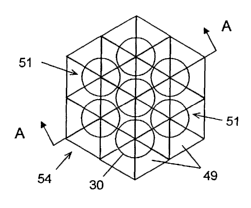
resolution. For cost reasons, the light sensors may have the arrangement 51
where each
2s light sensor views more than one crystal element 49 of a crystal array 54
as shown in Fig.
3a, but three light sensors may also have the arrangement 55 shown where three
light
sensors 30 are dedicated to each crystal segment 49 as shown in Fig. 3b. The
arrangement of Fig. 3b promotes a live crystal edge.
The light sensors may be coupled to the crystal directly without a window or
ao indirectly via a global window or via individual light pipes. Because the
crystal segments
are optically separated, at least in part, the fraction of light collected by
the three mutually
contiguous light sensors associated with a particular radiation event may be
improved
compared to no optical isolation among segments. The isolation directs some or
all of the
light from the radiation event to the three light sensors of interest.
Division of the crystal
ss into segments may improve rate capability in addition to light collection,
and for complete
-18-
CA 02442932 2003-10-03
WO 02/082122 PCT/US02/10375
cuts through the crystal foregoes the need for large, homogeneous crystals.
Variations in
response among the three light sensors allows for determination of the event
position all
the way to the edge of the triangular piece. Light collection and light
distribution properties
of the crystal and its optical system may be optimized to maximize the
precision with which
s event location is determined.
Combinations of the two light sensor arrangements 51 and 55 shown in Figs. 3a
and 3b may be used, depending on the application. For example, there could be
one light
sensor viewing several crystals in the center of an array, individual light
sensors viewing
only a single crystal near the edges, or an arrangement 56 using smaller area
light sensors
~0 57 (smaller diameter PMT's) as shown in Fig. 3c that would promote a live
edge.
As shown in Fig. 3e, the segmented arrays 54 shown in Figs. 3a, 3b and 3c may
be
manufactured by piecing together individual pieces 49' of crystal, possibly
selected for
performance criteria, to provide the segmented array 54'. The pieces of
crystal may be
bonded together at adjacent edges by a suitable adhesive 59 that preferably
also functions
as a reflector.
As shown in Fig. 3d, an array 54" may be fabricated by creating optically
isolating
slots 62 in a preexisting large crystal 63 and subsequently filling the slots
with appropriate
optical isolation or reflective material, or both, designed to tune the
response to desirable
characteristics. Similarly, the optical window 26" may have slots 67 formed
therein in a
2o pattern corresponding to the slots 62 in the crystal 63, and the slots 67
may be filled with
an optical isolation or reflective material. As will also be appreciated, a
slotted window like
that shown in Fig. 3d may also be employed with the composite crystal element
array 54'
shown in Fig. 3e, where the slots in the window correspond to the interfaces
between
adjacent crystal elements in the array.
2s The use of a segmented scintillator may provide one or more advantages. All
or
almost all of the light associated with a particular event may be collected
(in the case of
triangular segmentation) by only three light sensors rather than by a greater
number of light
sensors. This improves the statistics at each light sensor, resulting in more
accurate
results (less uncertainty). The field of view may also be extended to the
center of the
ao outside row of light sensors, since there does not need to be another row
of light sensors
for position detection in the peripheral region of the scintillator. Edge
effects (and the
resulting change in light response) are minimized, since all light sensors,
not just the
outside light sensors, see edge effects. Therefore, the light response should
be more
consistent light sensor-to-light sensor.
-19-
CA 02442932 2003-10-03
WO 02/082122 PCT/US02/10375
As noted above, a segmented scintillator is not required for triangular
mathematics
analysis. However, the use of a segmented scintillator provides advantage over
the use of
a single optically continuous scintillator. Triangular mathematics analysis,
or something
other that the presently-used standard method, may (if not must) be used with
segmented
crystals. With digital positioning techniques, the individual segments of the
optically
isolated variant may or may not have their light output gain matched
(normalized). In a
preferred embodiment, the response of each segment may be stored and used for
deriving
appropriate gain compensation information.
The collimator 22 (Fig. 1 a) associated with the scintillation crystal may
itself be
~o made with a triangular configuration and aligned so that collimator septa
are directly
opposite the slots or septa between individual crystal segments, which are a
radiation dead
region having no event occurrences.
The side edges of the crystal segments may be tapered so that they assemble
into
curved rather than flat shapes including, but not limited to, annular or domed
arrays.
Elements with tapered edges might be moved relative to one another in a final
product to
change the shape of the gamma camera detector for different clinical
applications. For
example, individual triangular crystal segments with tapered edges may be
mounted on a
flexible substrate that can be flexed to provide a desired shape of the
detector.
A conventional gamma camera may be improved by removing the optical window,
2o whether or not the scintillator is segmented. Elimination of the optical
window may reduce
the number of reflections encountered in the conventional camera and thereby
improve
light collection and localization of the light distribution. Elimination of
the window also may
allow for increasing the thickness of the crystal for achieving the desired
light spread
among light sensors, rather than using glass. Increasing the thickness may be
2s advantageous for high energy radiation detection such as that encountered
in PET
applications. When the window is removed, two of its typical functions may be
met by
other methods. Hermetic seals must be provided among or beyond the light
sensors. A
crystal support superstructure must also be provided, either among or beyond
the light
sensors or from the radiation side of the crystal.
ao Some of the improvements realized by eliminating the optical window may
also be
brought about by using a very thin window. The advantage of a thin window 79
is that it is
available for hermetic sealing, while leaving the advantage of a thick crystal
available for
light spreading and PET applications. A special low stress hermetic seal 80
may be used
with a thin window, as is shown in Fig. 4. A support superstructure 81
independent of the
ss window may still needed among or beyond the light sensors or provided by
the light
-20-
CA 02442932 2003-10-03
WO 02/082122 PCT/US02/10375
sensors. Otherwise, the assembly may need to be supported from the crystal
side, as is
illustrated in Fig. 4
According to another aspect of the invention providing for improved light
collection,
a conventional gamma camera detector or any of the above described
scintillator detector
arrangements may be improved by the addition of a reflector 70 aligned with
the spaces
between the PMT's 30 or other light sensors, as illustrated in Figs. 5a, 5b,
and 5c. The
light sensitive area of a PMT 30, called the cathode, only extends to the
inner glass side
wall 87 of the PMT. Moreover, cylindrical PMT's packed together have spaces
between
them even when packed together as closely as possible. Light reaching these
areas away
~o from the PMT cathodes (light sensitive area of the light sensors) generates
no signals and
is lost. Adding a reflector 70 in these areas as illustrated in Figs. 5a, 5b
and 5c improves
light collection. Improvement also occurs for arrays of hexagonal or square
light sensors,
such as PMT's since their glass walls do not contain cathode material.
The reflector 70 may be on the PMT side of the optical window 26 as seen in
Fig.
~s 5b, on the crystal side of the window, i.e., sandwiched between the
scintillator and the
window as seen in Fig. 5c. Less interference with optical coupling media is
possible on the
PMT side, but greater proximity to the light source and greater control of the
light
distribution occurs on the crystal side. In Fig. 5c, the reflector preferably
is in direct contact
with one or both of the scintillator and window.
2o A preferred reflector 70 is a non-specular (lambertian) reflective sheet
and
particularly a reflective sheet that can be applied without wetting of the
surface to which it
is applied. This is in contrast to a paint which has the disadvantage that it
wets the surface
to which it is applied, thereby negating the advantage of total internal
reflection.
A preferred reflector 70 is made of a material whose reflectivity will not be
degraded
25 by a significant amount by wetting with materials used to provide an
optical coupling
between the light sensors and the optical window or between the optical window
and the
scintillator, such as optical greases, adhesives and potting compounds.
Conventional
reflective materials, such as porous teflon, lose their reflectivity in these
situations. A
preferred reflector is one whose reflectivity does not degrade by more than
about 20%
so when wetted by the optical coupling material used at the interface where
the reflector is
installed (or when exposed to a potting material in general), and preferably
one that does
not degrade by more than about 10%. A particularly preferred reflector is a
white polyester
film, such as LumirrorT"~ polyester film sold by Toray Industries, Inc.
previously sold for use
as a reflector plate for LCD back-lighting applications. LumirrorT"" E60L
polyester film is a
-21-
CA 02442932 2003-10-03
WO 02/082122 PCT/US02/10375
white film with low specific gravity and high reflectivity, the typical
properties of which are
as follows:
Properties Unit Measurement
method
Thickness MMV Nm 188
Tensile strength MD MPa 107 ASTM D882
TD MPa 107 AS'TM D882
Elongation at Break MD % 85 ASTM D882
TD % 70 ASTM D882
~o Thermal Shrinkage MD % 1.4 ASTM D1204
at
(150C30min)
TD % 0.8 ASTM D1204
Whiteness Index % 130 ASTM E313
Specular Gloss % 25 ASTM D2457
~s Optical Density - 1.3 JIS K7605
Other polyester films doped with a white reflective filler material (such as
CaC03) are also
contemplated.
Moreover, the white polyester reflective film has applications in
scintillation
devices other than those specifically disclosed herein, such as radiation
detectors in
2o general which include a scintillator and a reflector disposed at a surface
(typically in
contiguous contact) of the scintillator for reflecting light. The scintillator
may be a
scintillation crystal, plastic scintillator, etc., depending on the particular
application. The
reflector may be a white polyester reflective film, pad, plate, etc.,
depending on the
particular application. Such a reflector may be exposed to a coupling or
potting
25 compound such as an oil, a silicone rubber, etc., without any significant
degradation of
the reflector's reflectivity, i.e., no greater than about 20% degradation. The
aforesaid
preferred LumirrorT"" polyester film when wetted by an optical coupling or
potting
compound affords a reduction of reflectivity no greater than about 10%, or no
greater
than about 5%, or less.
so The reflective sheet is provided with an array of openings for passing
light to the
light sensors. In the case where the reflective sheet is provided on the light
sensor side
of the optical window (or scintillator if no window is employed), the opening
(apertures)
preferably correspond in size and position to the active areas of the light
sensors and
specifically the photocathodes of PMT's. In the case where the reflective
sheet is
-22-
CA 02442932 2003-10-03
WO 02/082122 PCT/US02/10375
sandwiched between the optical window and scintillator, preferably the
apertures
preferably have an area no greater than and preferably less than the area of
the light
sensitive region of the respective light sensor.
In regard to the above-described triangular mathematics analysis and/or
s segmented scintillators, the light sensors may not have a uniform response
across the
light sensitive area thereof, such as across the photocathode of a PMT.
Therefore, the
light response function may vary not only from light sensor to light sensor,
but also over
the light sensitive area of a single light sensor. This may be compensated for
by mapping
the light sensitive area of the light sensors (e.g., the tube photocathodes)
and
~o incorporating this information into the event analysis in order to account
for such
variations. Also, the effects of events that are at light sensor centers or
along the seams
between scintillator segments may be compensated for during the event
analysis, as will
be appreciated by those of ordinary skill in the art.
Although the invention has been shown and described with respect to a certain
~5 preferred embodiment or embodiments, it is obvious that equivalent
alterations and
modifications will occur to others skilled in the art upon the reading and
understanding of
this specification and the annexed drawings. In particular regard to the
various functions
performed by the above described integers (components, assemblies, devices,
compositions, etc.), the terms (including a reference to a "means") used to
describe such
2o integers are intended to correspond, unless otherwise indicated, to any
integer which
performs the specified function of the described integer (i.e., that is
functionally
equivalent), even though not structurally equivalent to the disclosed
structure which
performs the function in the herein illustrated exemplary embodiment or
embodiments of
the invention. In addition, while a particular feature of the invention may
have been
25 described above with respect to only one of several illustrated
embodiments, such feature
may be combined with one or more other features of the other embodiments, as
may be
desired and advantageous for any given or particular application.
-23-