Note: Descriptions are shown in the official language in which they were submitted.
CA 02443582 2003-10-03
WO 02/082659 PCT/EP02/03596
ANALOGUE TO DIGITAL CONVERTER
This invention relates to an analogue to digital converter and a system for
controlling the envelope of a periodic waveform using such a converter.
Conventional commercially available integrated circuit analogue to digital
converters are only able to digitise signals up to approximately 1 GHz
bandwidth.
However, there is a requirement for digitising wide bandwidth periodic
analogue
electrical signals in a system that corrects ripple on the input signal. Such
signals
typically have a SGHz bandwidth or greater, which existing systems cannot deal
with.
In specialist test equipment, wide bandwidth signals up to 50GHz have been
digitised,
but the equipment is bulky, costly and has a high power requirement. These
drawbacks
make this type of equipment unsuitable for use in tightly integrated, low-
power systems.
Such prior art ADCs operate by sampling the input signal over a very short
time
window, and digitising the sample with a high resolution ADC that does not
have the
required input bandwidth. 'Equivalent-time sampling' is a technique that can
then be
used to measure the complete waveform.
There are existing A/D converters which operate by splitting an input signal
into
multiple signals and sampling these in parallel. This creates multiple high
fidelity
copies of the input signal. However, this method cannot be used at microwave
frequencies because of difficulties in sampling all the channels together.
In accordance with a first aspect of the present invention, an analogue to
digital
converter (ADC) comprises a comparator; an N x 1-bit clocked shift register;
and a
clock, wherein the clock is phase-locked to the input signal.
The present invention is able to take fast samples of the input signal,
convert
them to digital signals and subsequently store them in the shift register. The
stored
digital patterns may then be transmitted in parallel format at a significantly
lower rate.
The sampled signals can then be combined to build up a complete waveform. The
benefits of having the clock phase-locked to the input waveform are that the
representation of the input waveform can be built up over many repetitions of
it,
relaxing the requirements of the individual components comprising the ADC
implementation.
Preferably, the clock is a fixed frequency clock and the clock frequency is in
the
range of 1 GHz to SOGHz.
CA 02443582 2003-10-03
WO 02/082659 PCT/EP02/03596
2
Using a fixed frequency clock gives better fitter performance, since the
sample
interval is determined by the fixed frequency clock, rather than an
incremental delay as
used in conventional ADC. The clock frequency can certainly be lower than
IOGHz
(e.g. IGHz) without losing one of the essential features of the invention -
that it can be
realised using readily available low-cost commercially available components.
However
at lower clock frequencies e.g. lOkHz; alternative solutions are readily
available
because the problems of microwave operation do not apply.
Preferably, a threshold voltage applied to the comparator is varied in order
to
characterise an envelope of an input signal. Alternatively, a threshold
voltage applied to
the comparator is alternated between two nominated voltages, such that an
env;,lope of
an input signal is characterised more efficiently. Where the threshold voltage
is fixed, a
variable bias voltage may be applied to the input signal.
The ADC has a 1 bit resolution, but by varying the threshold level, it is
possible
to build up a more accurate representation of the signal. This is quite
different from the
mode of operation of prior art ADC's in the frequency range of interest.
Typically, the threshold voltage is generated by a processor controlled
digital to
analogue converter (DAC) circuit.
The input signal may have a bandwidth from d.c. up to 50GHz, and even higher
frequencies may be possible, but preferably, the input signal has a bandwidth
in the
range 1 GHz to 50 GHz.
Operating at microwave frequencies requires accurate matching of all
components in the system because the clock can be delayed by as much as the
signal
length. This problem does not occur at lower frequencies. One of the "hidden
features"
of prior-art "low-frequency" ADC architectures is that the propagation delay
between
the various discrete components is insignificant to overall operation. This is
a key
limitation when attempting to extend these techniques into the microwave
domain,
where the propagation delay between components can often exceed whole cycles
of the
ADC clock. Implementing an ADC at these microwave frequencies using existing
prior-
art ADC architectures with low-cost commercially available components is
therefore
impractical. This limitation is overcome in the system proposed in the present
invention.
In accordance with a second aspect of the present invention, a system for
controlling the envelope of a periodic waveform comprises an ADC according to
the
CA 02443582 2003-10-03
WO 02/082659 PCT/EP02/03596
first aspect and processing means, whereby the ADC samples an input waveform
and
the processing means determines a correction waveform, converts the correction
waveform to an analogue signal, combines the correction waveform with the
input
waveform to control its envelope and outputs a combined waveform, wherein the
combined waveform is substantially flat.
Alternatively, the combined waveform is substantially flat for a predetermined
portion of the input waveform.
In this context, flat is defined as being constrained between two threshold
voltages which are applied to the comparator alternately. By setting two
threshold
levels, it is possible to detect excursions of the output signal from 'flat',
and hence
modify the correction waveform to compensate.
It is common feature of comparator/shift register designs to have a sample
window which can be considerably shorter than the clock period. Thus, higher
bandwidth signals can be sampled by varying the phase of the clock signal
relative to
the input signal. This technique is called 'equivalent-time sampling'.
In this specification, the term bandwidth refers to the maximum bandwidth of a
signal which can be sampled and the term throughput refers to the number of
samples
which can be acquired per second.
An example of an analogue to digital converter and a system for controlling
the
envelope of a periodic waveform according to the present invention will now be
described with reference to the accompanying drawings in which:-
Figure 1 illustrates a system for controlling the envelope of a periodic
waveform;
Figure 2 illustrates examples of how the clock is phase locked to the input
signal; and,
Figure 3 illustrates a digital to analogue converter according to the present
invention for use in the system of Fig. 1.
One example of a system according to the present invention is shown in Fig. 1.
The system comprises a voltage-controlled attenuator 1 which receives an input
signal
2. The input signal 2 has peaks and troughs which need to be flattened out to
produce a
substantially constant output level. An output from the attenuator 1 is split
in a sputter
3, so that one output of the sputter forms the output signal 4 and another
output from
CA 02443582 2003-10-03
WO 02/082659 PCT/EP02/03596
4
the sputter is input to an analogue to digital converter (ADC) 5 in accordance
with the
invention. A digital signal output from the ADC 5 is processed by a processor
6, input
to memory 7 and under control of a clock 8, successive values in the memory 7
are
passed through a digital to analogue converter (DAC) 9, filtered by a low pass
filter 10
and the filtered signal applied to the control input of the voltage controlled
attenuator 1.
The system operates by sampling a portion of the output from the attenuator 1
and digitising the sampled signal. The loop bandwidth is, greater than any
variation in
input signal between successive periods. Because of this the system is able to
track any
variations, and thus produce a substantially flat output. Because the output
is
substantially flat, an ADC with only one bit resolution is required to
characterise it, thus
simplifying the hardware. The processor 6 calculates a correction waveform
which
when combined with the input waveform produces a substantially constant
waveform.
Data representing the correction waveform is passed to the memory 7.
Successive
values in memory are passed to the DAC 9 at a rate which is controlled by the
clock 8
which is phase-locked to the input signal 2. The resulting analogue waveform
is then
low-pass filtered by filter 10 to produce waveform 12 which is used to control
the
attenuator l, and thus to control the shape of the output signal 4.
In Fig. 2a, a first example of how the clock is phase-locked to the input
signal is
shown. In this case, it can be seen that both the input signal and the clock
are similarly
regular and each clock cycle coincides with a similar point on a cycle of the
input
signal. In Fig. 2b, the input signal is still regular, but it is spread out
over a longer
period of time, so that the repetition occurs after several clock cycles,
rather than every
one.
A particular feature of this invention is the design of the ADC 5.
Conventional
ADC integrated circuits are capable of digitising signals with bandwidths up
to
approximately IGHz. However, there is a requirement to digitise periodic
analogue
electrical signals for which these conventional ADC integrated circuits are
not suitable,
for example, flattening the waveform produced by a pulsed chirp laser. This is
particularly applicable to telecomms applications. Analogue to digital
conversion
systems, which are capable of sampling up to 50GHz bandwidth, have been
produced
but these are bulky and expensive, so are not suitable for this application.
Also, because
they are not available as integrated circuits due to their complexity and high
performance, they cannot be incorporated easily into existing system designs.
These
CA 02443582 2003-10-03
WO 02/082659 PCT/EP02/03596
conventional ADC's rely on equivalent-time sampling techniques to achieve the
required bandwidth.
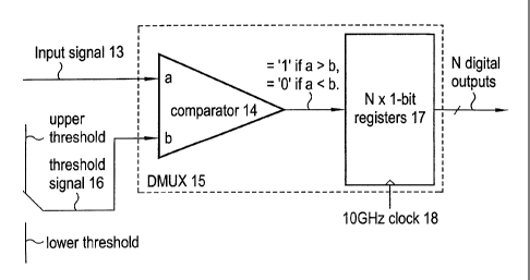
The present invention overcomes the problems of conventional systems dealing
with wide bandwidth signals by using a demultiplexer circuit as a combined 1-
bit ADC
5 (or comparator) and N x 1-bit register, as shown in Fig. 3. 1n this
particular example,
the demultiplexer (DMUX) 15 is a 16:1 DMUX (i.e. N = 16) operating at
approximately
IOGHz, but higher clock rates, e.g. 40GHz, and other ratios, e.g. 4:1 or 2:1
are also
currently available. A sampled signal 13 from the sputter 3 is applied to
input a of the
comparator 14 in the DMUX 15. A threshold signal 16 is applied to input b of
the
comparator 14. The threshold signal voltage may be generated by a DAC circuit
under
control of the processor 6. The sampled waveform is periodic, so that it is
not essential
to sample every single cycle. This feature allows a low speed DAC to be used
to
generate the threshold signal voltage, because samples can be discarded whilst
the DAC
settles. The output of the comparator 14 is logical "1" if input a is greater
than input b
and logical "0" otherwise. The output values are stored sequentially in the 16
x 1-bit
register 17 on successive rising edges of the clock 18.
In a preferred mode of operation, 1-bit digitised samples of the analogue
input
signal from the register 17 are sent to the processor 6, sixteen at a time
corresponding to
sixteen consecutive samples. The processor 6 can then determine which portions
of the
waveform are above or below the threshold voltage and alter the values in the
memory 7
accordingly thus changing the correction waveform. By setting alternately high
and low
threshold voltages, the output signal can be constrained between the two
threshold
levels.
An alternative mode of operation requires only one threshold level 16 to be
set.
In this mode the processor 6 counts the number of ones and zeros corresponding
to the
same sample instant in the cycle. The ratio of ones to zeros is used to
determine the
appropriate corresponding value in the memory 7; thus changing the correction
waveform to maintain the ratio at approximately 50:50.
The system of the present invention produces an output signal which is
substantially flat. An alternative is to produce an output signal which is
substantially
flat for a particular portion of its period by modifying selected entries in
the memory 7.
Amongst the advantages of the ADC of the present invention are that it uses a
small, low-cost, low-power commercially available device compared to existing
ADC's
CA 02443582 2003-10-03
WO 02/082659 PCT/EP02/03596
6
which operate at these bandwidths; it offers improved fitter performance since
the
sample interval is determined by a fixed-frequency clock, rather than the
conventional
method of using an incremental delay; and it offers full bandwidth performance
at 1-bit
resolution as compared with the significantly smaller bandwidths offered by
conventional devices, albeit at higher resolution.