Note: Descriptions are shown in the official language in which they were submitted.
CA 02443782 2003-10-10
WO 02/089907 PCT/AU02/00575
1
Process for manufacturing electrically conductive components'
Field of the Invention
The present invention relates to a method of forming miniature wiring
and connector systems for electrical products. More specifically the present
invention relates to a method of forming electrode arrays, such as arrays for
sensors, including biosensors, and implantable devices, such as an implantable
recording or stimulating electrode or pad for use in the body. An electrode
Zo array formed using the method is also described.
Background of the Invention
In many electrical devices, particularly those that are manufactured on a
very small scale, the manufacture of the wiring and connector components is
often a labour intensive and specialised craft. Ensuring that the wiring and
connection of the various components of the systems occurs correctly is often
the most expensive and labour intensive aspect of the manufacturing process,
resulting in large costs associated with the time taken to manufacture the
2o device which is often passed on to the ultimate consumer. This is also the
case When such devices need to be specifically hand made to a specification
as often the availability of the device is dependant upon the time taken to
manufacture the device, with the time taken being difficult or impossible to
expedite.
This is particularly the case in the field of medical implants and electrical
devices that are implanted in the body to perform a specific task. Such
devices
may include: stimulating devices such as pacemakers, cochlear implants, FES
stimulators; recording devices such as neural activity sensors and the like;
3o implantable cables which may be used to connect implantable devices to
other
implantable devices or stimulatinglsensing devices; diagnostic devices capable
of carrying out in-vivo analysis of body parameters; and other types of
implantable devices not yet contemplated. In such devices, the size needs to
be minimised to ensure that they are minimally invasive upon implantation. As
a result, in such instances, the electronic wiring and connections need also
to
be relatively very small. As such, manufacturing such devices to ensure that
CA 02443782 2003-10-10
WO 02/089907 PCT/AU02/00575
2
they are reliable and sturdy is a specialised art, and requires much time and
expense.
As a result of the need to increase the miniaturisation of such devices, a
wide range of techniques have been developed to create patterned
components which would be too difficult or impossible to create by hand design
and satisfy the high volume supply required. Techniques such as
electroforming, vacuum deposition (sputtering, evaporation), and chemical
vapour deposition, to name a few, are some of the known ways to produce
Zo patterned electrically conductive features on insulating surfaces on a
micron
scale. The problem with such methods however, has been that the metallic
films produced by these techniques have been shown to feature properties that
are different from the corresponding properties of the bulk materials used.
This
results in the desired materials functioning difFerently from their intended
1s purpose, and in the particular case of platinum, the thin films have tended
to
crack and exhibit large impedance as well as a high degree of delamination.
In the manufacture of such devices, the bulk material is chosen based on
the properties it exhibits. In the case of implantable electrical components,
2o platinum has been found to exhibit particularly useful properties for such
an
application, namely good conductivity and inertness. With this being
understood, it is beneficial in the manufacture of such devices for the bulk
material to exhibit the same properties, especially physical properties, after
manufacture as it did prior to manufacture, as discussed above. Variations in
25 these properties can have a bearing on the functionality of the device,
which,
particularly in medical implanted devices, is highly undesirable. As
mentioned,
platinum films tend to crack and delaminate, hence delivering high impedance
which impairs the functionality of the device. The use of thin film technology
has been shown to work for a number of materials such as copper, gold and
3o nickel, however none of these materials are suitable for active implantable
devices.
Other more conventional methods of manufacturing such devices would
be to directly stamp the desired components out of a conductive sheet using a
35 fine blanking or stamping method. This is possible for applications whereby
single components having large dimensions are stamped and the components
CA 02443782 2003-10-10
WO 02/089907 PCT/AU02/00575
3
do not need to be thin and flexible. However, simple stamping techniques are
not suitable for multiple components having very small dimensions made out of
thin conductive sheets, such as those proposed to be covered by the present
invention. In such applications, the fine width dimensions of the components
and between the components are too small for stamping machines and the
sheet material is too thin to provide the precision required for such
components.
Because of these problems, medical implants, such as cochlear
Zo implants, are still manufactured using labour intensive manual procedures.
Hearing loss, which may be due to many different causes, is generally of
two types, conductive and sensorineural. In some cases, a person may have
hearing loss of both types. Of these types, conductive hearing loss occurs
z5 where the normal mechanical pathways for sound to reach the hair cells in
the
cochlea are impeded, for example, by damage to the ossicles. Conductive
hearing loss may often be helped by use of conventional hearing aids, which
amplify sound so that acoustic information does reach the cochlea and the hair
cells.
In many people who are profoundly deaf, however, the reason for their
deafness is sensorineural hearing loss. This type of hearing loss is due to
the
absence of, or destruction of, the hair cells in the cochlea which transduce
acoustic signals into nerve impulses. These people are thus unable to derive
suitable benefit from conventional hearing aid systems, no matter how loud the
acoustic stimulus is made, because there is damage to or absence of the
mechanism for nerve impulses to be generated from sound in the normal
manner.
3o It is for this purpose that cochlear implant systems have been developed.
Such systems bypass the hair cells in the cochlea and directly deliver
electrical
stimulation to the auditory nerve fibres, thereby allowing the brain to
perceive a
hearing sensation resembling the natural hearing sensation normally delivered
to the auditory nerve. US Patent 4532930, the contents of which are
incorporated herein by reference, provides a description of one type of
traditional cochlear implant system.
CA 02443782 2003-10-10
WO 02/089907 PCT/AU02/00575
4
Typically, cochlear implant systems have consisted of essentially two
components, an external component commonly referred to as a processor unit
and an internal implanted component commonly referred to as a
receiver/stimulator unit. Traditionally, both of these components have
cooperated together to provide the sound sensation to a user.
The external component has traditionally consisted of a microphone for
detecting sounds, such as speech and environmental sounds, a speech
Zo processor that converts speech into a coded signal, a power source such as
a
battery, and an external transmitter coil.
The coded signal output by the sound processor is transmitted
transcutaneously to the implanted receiver/stimulator unit situated within a
recess of the temporal bone of the user. This transcutaneous transmission
occurs via the external transmitter coil that is positioned to communicate
with
an implanted receiver coil provided with the receiver/stimulator unit. This
communication serves two essential purposes, firstly to transcutaneously
transmit the coded sound signal and secondly to provide power to the
2o implanted receiver/stimulator unit. Conventionally, this link has been in
the
form of a radio frequency (RF) link, but other such links have been proposed
and implemented with varying degrees of success.
The implanted receiver/stimulator unit traditionally includes a receiver
coil that receives the coded signal and power from the external processor
component, and a stimulator that processes the coded signal and outputs a
stimulation signal to an intracochlea electrode assembly which applies the
electrical stimulation directly to the auditory nerve producing a hearing
sensation corresponding to the original detected sound.
It is known in the art that the cochlea is tonotopically mapped. In other
words, the cochlea can be partitioned into regions, with each region being
responsive to signals in a particular frequency range. This property of the
cochlea is exploited by providing the electrode assembly with an array of
3s electrodes or stimulating pads, each electrode or pad being arranged and
constructed to deliver a stimulating signal within a preselected frequency
range
CA 02443782 2003-10-10
WO 02/089907 PCT/AU02/00575
to the appropriate cochlea region. The electrical currents and electric fields
from each electrode or pad stimulate the nerves disposed on the modiolus of
the cochlea. As the size of the cochlea is very small and the electrode
assembly needs to be flexible enough to be inserted into the cochlea, the
5 dimensions of the electrode assembly are such that do not allow for
traditional
manufacturing techniques.
For this reason, the intracochlear electrode array has generally been
formed in a manual process by positioning a plurality (eg. 22) of electrically
Zo conductive platinum rings in a linear array and then welding electrical
conductive wires to each of the electrodes or pads. This process can lead to
small variations in the locations of the electrodes or pads and wiring from
one
manufactured array to the next with consequent small variations in the overall
mechanical properties of the array once a resiliently flexible carrier member
is
i5 moulded about the array. Each of the wires require connection to the
receiver/stimulator unit and in order to ensure system integrity, each of the
wires have been insulated from the others so that unwanted interaction
between different electrical components is eliminated.
2o While the above method has proven very successful, it is labour
intensive and hence a relatively expensive process. With implanted devices
and miniaturisation becoming more common, there is an increasing need to
provide electronic wiring and electronic connections in such systems that are
both simple and reliable. The present invention is directed to a new method of
25 forming such wiring and connections that addresses at least some of the
problems with prior art processes.
Any discussion of documents, acts, materials, devices, articles or the like
which has been included in the present specification is solely for the purpose
of
3o providing a context for the present invention. It is not to be taken as an
admission that any or all of these matters form part of the prior art base or
were
common general knowledge in the field relevant to the present invention as it
existed before the priority date of each claim of this application.
CA 02443782 2003-10-10
WO 02/089907 PCT/AU02/00575
6
Summary of the Invention
Throughout this specification the word "comprise", or variations such as
"comprises" or "comprising", will be understood to imply the inclusion of a
stated element, integer or step, or group of elements, integers or steps, but
not
the exclusion of any other element, integer or step, or group of elements,
integers or steps.
1o The present invention enables the manufacture of a multiplicity of
components, where position of the individual components with respect to each
other is predetermined and kept constant throughout the process, including the
assembled final product. This is achieved without the use of traditional
methods such as fine blanking and thin film technologylphotolithography. The
present invention relates to a method of manufacture of patterned features in
the domain of microtechnology, wherein the properties of the chosen bulk metal
are maintained throughout the manufacture of the device. The present
invention also resides in a multilayered assembly and the method of assembly
of the multilayered assembly.
The present application is directed to a method of forming electrical
components for an electrical device. The method provides an advantage over
the prior art in that it enables multiple electrical components to be formed
in a
simple and efficient manner, using materials and dimensions not possible with
traditional mass production forming methods. The invention uses a sheet of
material whose properties do not allow stamping out line widths as narrow as
are required in the final assembly and allows multiple miniature components to
be formed in very close proximity of dimensions not achievable through
traditional stamping processes.
In a preferred embodiment, the present application is directed to a
method of forming an electrode array for an electrode assembly. The method
has potential advantages in providing a more efficient and inexpensive process
of electrode assembly manufacture, particularly assembly of intracochlea
electrode assemblies. The present invention further provides a method of
forming an electrode array for an electrode assembly that preferably allows
the
CA 02443782 2003-10-10
WO 02/089907 PCT/AU02/00575
7
manufacturing process to become automated or semi-automated so providing a
desirable alternative to current manufacturing processes which require
extensive labour input and increased manufacturing throughput.
In a first aspect, the present invention is a method of forming a device
comprised of a predetermined pattern of relatively electrically conductive
regions and relatively electrically resistive regions, the method comprising a
step of:
(a) working a sheet of electrically conductive material to remove
Zo predetermined portions therefrom to form said one or more discrete
relatively
conducting regions.
In this aspect, the step of working the sheet can include a step of
pressing a sheet of electrically conductive material to form a predetermined
i5 raised pattern therein. One or more of the raised portions of the sheet can
then, preferably, be removed to leave a remaining portion having a
predetermined pattern. In another embodiment, those portions of the sheet not
raised during the pressing step can be removed to leave a remaining portion
having a predetermined pattern. In a still further embodiment, at least some
of
2o the raised pattern and at least some of the unraised portion can be removed
to
leave a remaining portion having a predetermined pattern.
Still further, the step of working the sheet can include a step of punching
portions out of the sheet of electrically conductive material. In this
25 embodiment, portions of the sheet are removed and separated from the sheet.
Yet further, the step of working the sheet can include a step of slicing or
cutting the sheet of electrically conductive material.
3o In one embodiment, the remaining portion formed by the method can be
used as an electrode array or a portion thereof. For example, the method can
be used to form a layered component of an electrode array. The electrode
array can comprise a plurality of stimulating pads or electrodes.
35 In yet another embodiment, the method can comprise an additional step
of placing said remaining portion on a flexible carrier. Still further, the
method
CA 02443782 2003-10-10
WO 02/089907 PCT/AU02/00575
8
can comprise the step of placing a plurality of said remaining portions on a
flexible carrier. to form an electrode array. In this embodiment, the
plurality of
remaining portions can be adapted to be formed into a layered configuration to
form one or more electrode arrays.
In a preferred embodiment, the electrode array is for use as an
implantable tissue-stimulating device. More preferably, the tissue-stimulating
device is a cochlear electrode assembly, more preferably an intracochlear
electrode assembly. In another embodiment, the electrode array could be used
Zo in a biosensor not necessarily related to an implanted device.
In one embodiment, the sheet of electrically conductive material is a
biocompatible material. In a preferred embodiment, the sheet is a metallic
material. Still further, the metallic material is a sheet of platinum. In a
further
i5 embodiment, the sheet can be annealed. In a further embodiment, the
electrode array is formed from a single sheet of electrically conductive
material,
such as platinum. In a further embodiment, more than one array can be formed
from a single sheet of platinum. In yet a further embodiment the sheet could
be
a laminate of two or more layers (eg Pt & Ir), or could be an alloy.
The sheet preferably has a thickness between about 1 and 100 microns,
more preferably between about 10 and 50 microns. The method preferably
uses a sheet of platinum having a thickness no greater than 50 microns, more
preferably no greater than 20 microns. Other suitable thicknesses can be
envisaged. Each sheet can have dimensions of about 50mm x 250mm. The
size of the sheet will though depend on the requirements of the tooling used
to
work the sheet. As such, sheets of different dimensions can be envisaged.
Generally it has been found that traditional stamping techniques have proven
difficult to perform with the required accuracy upon sheets of material less
than
50 microns, where the presence of a shear lip is a problem.
Still further, a plurality of electrically conducting connecting means can
extend away from the stimulating pads of the electrode array. Eaoh stimulating
pad of the electrode array preferably has at least one connecting means
extending away therefrom. More than one connecting means can extend from
some or all of the stimulating pads in the electrode array.
CA 02443782 2003-10-10
WO 02/089907 PCT/AU02/00575
9
The connecting means are preferably linearly aligned for a majority of
their length extending away from the electrode array. In one embodiment, the
connecting means can be disposed for at least a portion of their lengths in a
parallel arrangement. Where the electrode array is formed from a single sheet,
the plurality of connecting means are also preferably formed from that sheet
and are integrally connected to respective electrodes in the array.
The sheet of conductive material can before the working step be a planar
Zo sheet. Sheets that already have folds or embossments formed therein prior
to
the working step of the present invention can, however, also be envisaged.
In producing an electrode array, it is firstly desirable to determine the
configuration of the stimulating pads desired for the electrode array. Once
the
configuration is determined, the step of working the sheet can comprise using
an embossing tool that is fabricated for use in the method so as to produce
the
desired electrode array configuration. Details of one possible type of
embossing tool will be provided in more detail below.
2o In a preferred process, a planar sheet is placed relative to an embossing
tool in a pressing means. The pressing means can be programmable to press
a predetermined pattern in the sheet. Where the embossing tool is horizontally
or substantially horizontally aligned, the planar sheet can be placed
relatively
above the embossing tool or relatively below the embossing tool. Where the
embossing tool is vertically or substantially vertically aligned, the planar
sheet
can also be disposed in a vertical or substantially vertical alignment beside
the
embossing tool.
In one embodiment, the planar sheet can be moved relative to the
so embossing means and the pressing means and so be brought into position
within the pressing means. In another embodiment, the embossing means
and/or the pressing means can be moved relative to the planar sheet to
relatively bring the planar sheet within the pressing means. In one
embodiment, the process can be a continuous process, wherein a continuous
sheet is fed through the pressing means.
CA 02443782 2003-10-10
WO 02/089907 PCT/AU02/00575
The pressing means can include any medium having suitable properties
to press the sheet of material and form the raised pattern therein. In one
embodiment, the pressing means can be formed of a material with relatively
low compressibility, such as a liquid, or gel having a relatively high content
of
5 liquid whilst retaining sufficient fluidity to occupy the available space.
In
another embodiment, compressed gas can be used to press the planar sheet
against the embossing tool.
In one embodiment, the raised pattern is formed by a single pressing of
1o the sheet. In another embodiment, the raised pattern can be formed by two
or
more pressings of the sheet. Where the raised pattern is formed by two or
more pressings, the second or greater pressing of the sheet can be performed
by the same embossing tool or a different embossing tool to that used for the
first pressing. Where there are two or more pressings, the sheet may remain
stationary between pressings or be relatively moved to a new press for each
pressing of the sheet.
In a preferred embodiment, the pressing means used in the method has
at least one relatively movable platen. The relatively movable platen
preferably
2o moves relative to a stationary platen. The embossing tool is preferably
mounted to the stationary platen of the press.
Where the platens are horizontally disposed, the lower platen is
preferably stationary and the upper platen preferably moves downwardly and
upwardly relative to this stationary platen. In this embodiment, the embossing
tool is preferably placed on the lower platen.
In one embodiment of the method, the sheet is placed above and on the
embossing tool. A layer of backing material is then placed on top of the sheet
3o before operation of the press. The layer of backing material can comprise a
layer of a resiliently flexible polymeric or elastomeric material. The backing
material can comprise a sheet of silicone or rubber and in another embodiment
the backing material can be used as an integral part of the device. In a
situation where the backing material is used as an integral part of the
electrode
array, the backing material must be suitable for implantation purposes, eg
silicone.
CA 02443782 2003-10-10
WO 02/089907 PCT/AU02/00575
11
In another embodiment, a lubricant can be used to improve the quality of
embossed pattern. The lubricant is preferably suitable for an implant to avoid
the cleaning step. Ethanol could be a suitable lubricant since it evaporates
quickly and is in fact used as a washing agent in the assembly of implantable
devices. A thin layer of the lubricant can be present between the embossing
tool and the foil, and between the foil and the backing, or preferably both.
The pressing means can preferably apply differing levels of pressure to
1o the sheet of the electrically conducting material placed on the embossing
tool.
For example, the pressing means can apply an initial pressure for a first
predetermined period of time and then apply a second different pressure for a
further predetermined period of time. The second pressure can be greater or
lower than the initial pressure. The further predetermined period of time can
also be less than, greater than or the same as the first predetermined period
of
time. In another embodiment, the pressure applied by the pressing means can
continue to gradually increase throughout the embossing step.
In the method, the embossing tool with the embossed sheet and
2o protective layer positioned thereon, can be relatively removed from within
the
pressing means. Following pressing of the sheet of electrically conducting
material, the layer of protective material can be removed from the embossed
sheet. The layer of protective material is preferably removed from the
embossed sheet before the sheet is removed from the embossing tool. In
2s another embodiment, the protective layer is retained on the sheet through
later
processing steps.
As described, once the sheet has been pressed to form a raised pattern
therein, unwanted portions of the sheet can be removed. The unwanted
3o portions can be removed by any number of ways, such as by cutting or by an
abrading means.
It is envisaged that the cutting step can be performed at the same time
as the pressing of the sheet of the conductive material. In this case the
35 pressure applied to the sheet can be adjusted so as to be sufficient to
cause
the cutting of the sheet over the sharp edges of the embossing tool. In such
an
CA 02443782 2003-10-10
WO 02/089907 PCT/AU02/00575
12
embodiment, the embossing tool is design to feature sharp edges that favour
cutting the sheet. The cutting step is preferably performed relatively
quickly. In
a further embodiment, the sheet is preferably cooled prior to cutting. In one
embodiment, the sheet can be cooled by liquid nitrogen prior to cutting.
In a still further embodiment, the sheet can be clamped to the embossing
tool at the location of the protrusions of the tool.
The abrading means can preferably abrade or grind the unwanted
Zo portions from the sheet. It will be appreciated that the step of abrading
the
unwanted portions of the sheet may comprise more than one step. For
example, a relatively coarse first abrading step may be firstly performed to
move relatively large pieces of the unwanted portion of the sheet. Once this
first step is complete, removal of finer pieces can be made by one or more
i5 additional abrading or polishing steps. In one embodiment, each additional
abrading step removes finer pieces of the sheet than the preceding step.
These additional steps ensure that the dimensions and shape of the remaining
portions of the sheet match the originally desired configuration.
2o To prepare the embossed sheet for removal of the unwanted portion, the
embossed sheet can be adhered by a layer of an adhesive to a support base.
The adhesive is preferably a material that can be used to reversibly anchor
the
embossed sheet to the base. In one embodiment a PVA (polyvinyl alcohol)
based adhesive is used that can hold the embossed sheet in place and, after
25 the removal of the unwanted material, can be dissolved in water, freeing
the
said structure. In another embodiment, the preferred adhesive is an
electrodisbonding adhesive. In this case, the support base must be
electrically
conducting. The support base can be formed from a group consisting of high
alloy steel, carbon steel, stainless steel, aluminium, aluminium alloys,
copper,
ao and titanium.
In one embodiment, the electrodisbonding adhesive is an epoxy resin
formulation capable of forming relatively high strength adhesive bonds with
conductive substrates but which can be relatively rapidly released through the
s5 application of a low voltage current. Disbonding preferably occurs via
CA 02443782 2003-10-10
WO 02/089907 PCT/AU02/00575
13
electrochemical reactions induced at the interface between the cured adhesive
and the bonded substrate.
To adhere the embossed sheet to the support base, a quantity of
adhesive is preferably firstly placed on a surface of the support base.
Support
spacers for a top plate are preferably positioned on the base plate around the
border of the adhesive. The spacers can be relatively short. For example, the
spacers can have a height of between about 1 and 1000 microns, more
preferably about 150 microns.
Once the adhesive and spacers are in place, the embossed sheet is
preferably placed on the adhesive. In one embodiment, the embossed sheet is
placed on the adhesive such that the raised pattern extends outwardly away
from the adhesive. In an alternative embodiment, the embossed sheet is
placed on the adhesive such that the raised pattern extends inwardly into the
adhesive.
Once the embossed sheet is in position, a top plate is then preferably
placed on top of the embossed sheet and pressed downwardly until it rests on
2o the spacers. The top plate is preferably formed from the same material as
the
base plate. A different material for the top plate could, however, be
utilised.
The top and bottom plate should be substantially parallel with respect to each
other.
Once the adhesive is cured, the top plate and spacers can be removed.
The support base, with the embossed sheet adhered thereto, is then ready to
undergo further processing as defined above.
Where the raised pattern extends outwardly away from the support base,
3o the abrading means will preferably remove a portion of the raised pattern
formed in the sheet. Where the raised pattern extends inwardly into the
adhesive, the non-raised portion of the sheet, or at least a portion thereof,
will
preferably be removed by the abrading means.
The remaining portion of the sheet left after the abrading step preferably
comprises a plurality of electrically independent portions that preferably
serve
CA 02443782 2003-10-10
WO 02/089907 PCT/AU02/00575
14
as stimulating pads of the electrode array. Where desired, the remaining
portion also serves to provide the electrical connection means to the formed
stimulating pads.
As previously defined, the step of working the sheet can include a step of
punching portions out of the sheet of electrically conductive material. In one
embodiment, the sheet of electrically conductive material, such as the
platinum
sheet defined herein, can be coated on a layer of resiliently flexible
material,
preferably a biocompatible resiliently flexible material like a silicone. A
punch
1o means fabricated so as to punch out a desired portion of the sheet is
preferably
brought into engagement with the sheet and punches out a desired portion. In
a preferred embodiment, the stroke of the punch is such that the punch pushes
the desired portion into the silicone layer where it can remain embedded.
In one embodiment, the step of punching out portions can comprise one
use of a punch. In another embodiment, multiple uses of a punch may be
necessary to form a predetermined pattern in a sheet. In another embodiment,
the punch can be adapted to punch different portions of the sheet to different
levels within the resiliently flexible layer.
This embodiment has the advantage of potentially forming two or more
conductive layers from a single sheet of electrically conductive material.
As also previously defined, the step of working the sheet can include a
step of slicing or cutting the sheet of electrically conductive material. In
this
embodiment, a cutting or slicing tool can be fabricated to form appropriate
cuts
in the sheet of electrically conductive material so resulting in the formation
of a
predetermined pattern of electrically conductive regions. In using such a
tool,
the sheet of electrically conductive material, such as the platinum sheet
defined
3o herein, can be coated on a layer of resiliently flexible material,
preferably a
biocompatible resiliently flexible material like a silicone. The cutting tool
can be
constructed so as to be relatively driven into contact with the surface of the
platinum sheet. The tool can further be fabricated so as to drive at least a
portion of the sheet into the resiliently flexible material.
CA 02443782 2003-10-10
WO 02/089907 PCT/AU02/00575
In one embodiment, the method can further include the step of
encapsulating at least one surface of the embossed sheet. In a preferred
embodiment, the abraded surface of the sheet can be encapsulated in an
electrically insulating material. This material is further also preferably
5 bicompatible and resiliently flexible. One example of a possible
encapsulating
material is silicone.
Once the silicone is cured, the subassembly is removed from the
"reversible" adhesive. In the case of the PVA adhesive, this can be removed
1o by applying a certain quantity of water to dissolve away the PVA-based
adhesive.
Once disbonded, the result is a plurality of separate electrically
independent conductive portions having a layer of silicone encapsulated on one
15 side thereof. If desired, the formed electrode array can undergo further
processing, including washing and drying, to render it suitable for
implantation
as an intracochlea electrode assembly.
In another embodiment, the embossing tool can be retained in contact
2o with the sheet of electrically conductive material. With the embossing tool
in
place against one face of the embossed sheet, the other face of the sheet can
be encapsulated with at least a first layer of resiliently flexible material.
This
layer of material can comprise a layer of a polymeric or elastomeric material,
such as a silicone or rubber. In a further embodiment, more than one layer of
encapsulating material can be coated on the other face of the embossed sheet.
The selected encapsulating material is preferably adapted to adhere strongly
to
the other face of the sheet. If necessary, a suitable silicone/metal adhesive
can
be used to ensure the encapsulating silicone layer remains in contact with the
other face on subsequent removal of the embossing tool from said one face of
3o the sheet.
With the embossing tool removed, the one face can then be subject to
the abrading step of the process with at least a portion of the sheet not
comprising part of the raised pattern therein being abraded from the sheet. if
necessary, the encapsulation on the other face of the sheet can be rapidly
CA 02443782 2003-10-10
WO 02/089907 PCT/AU02/00575
16
cooled, such as by immersion in liquid nitrogen, to stiffen and harden the
encapsulation prior to and/or while the abrading step is being performed.
In another embodiment, the removal of the embossing tool is not
required. The embossed sheet in this embodiment is kept in close proximity of
the embossing tool after the embossing process. In this embodiment the
embossing tool is a disposable item and it is preferably fabricated using a
low
cost process to minimise the cost thereof.
1o As a result of the abrading step, a plurality of electrically separated
stimulating pads and appropriate conducting means for each pad are formed.
A layer of silicone or other suitable resiliently flexible and preferably
biocompatible material is then used to form an encapsulation of the abraded
side of the sheet. While this layer of encapsulation should encapsulate the
electrical conduction means, it is preferred that the formed stimulating pads
are
not encapsulated. Accordingly, the mould used in the moulding of this
encapsulation can incorporate upstanding insets that extend outwardly from the
mould and which are aligned with the positions of the formed stimulating pads.
These insets preferably abut the pads and so prevent the encapsulation
2o covering the pads during the encapsulating process.
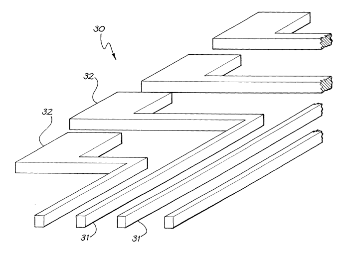
In one embodiment, two or more arrays formed using the method can be
laminated together to form a single tissue stimulating electrode assembly. In
one embodiment, the assembly can be formed from a first lamination having 7
electrodes, a second lamination having 8 electrodes and a third lamination
having 8 electrodes, to form an electrode assembly having 23 electrodes. In
the case of a cochlear electrode array, the formed array will preferably have
22
intracochlea electrodes and one extracochlea electrode. Such a lamination
process preferably results in a linear array of the 22 electrodes.
In a further aspect, the present invention is an embossing tool for use in
the method as defined herein.
In a preferred embodiment of this aspect, the tool is formed from a
3s material that will emboss the electrically conducting sheet used in the
method.
Where the sheet is thin platinum sheet, the embossing tool can be formed from
CA 02443782 2003-10-10
WO 02/089907 PCT/AU02/00575
17
a metal material, such as a copper, or another material such as silicon wafer,
or
suitable plastics such as polycarbonate or polyimide.
The embossing tool will have a plurality of protrusions formed therein.
The shape, dimension and position of the protrusions represent the raised
pattern to be formed in the sheet of electrically conducting material. In the
case
of the silicon wafer, the protrusions can be etched in the wafer. In the case
of a
metallic embossing tool, the protrusions can be fabricated through use of
laser
micromachining. The plurality of protrusions can be adapted to form
1o embossments in the sheet that are later removed from the sheet. In another
embodiment, the protrusions can be adapted to form embossments that are not
later removed from the sheet.
As an example only, to form a plurality of parallel linearly disposed
1~ electrical conduction means, the embossing tool preferably has a series of
protrusions extending for a length in side-by-side relationship. The
protrusions
can narrow in thickness from their base to their top. In one embodiment, each
protrusion at its base can have a thickness of between about 48 and 54
microns. At the top, each protrusion can have narrowed in thickness to
between about 28 and 30 microns. The distance between adjacent protrusions
at the base can be between about 65 and 67 microns, while the distance
between the protrusions at the top is between about 86 and 87 microns. Each
protrusion can have a height of about 30 microns.
25 Each ridge preferably ends in a pad protrusion adapted to emboss the
electrically conductive sheet in a manner suitable to form a stimulating pad.
The protrusion is preferably substantially rectangular in shape. To allow the
formation of a longitudinal electrode array, each ridge preferably turns just
prior
to its join with its respective electrode protrusion. The turn in the ridge
can be
so smoothly curved.
In a further embodiment, the plurality of aligned protrusions for the
electrical conduction means extend linearly away from the pad protrusions for
a
length. The protrusions then further preferably spiral inwardly in ever
35 decreasing circles. At an end distal the pad protrusion, each protrusion
preferably terminates in a feedthrough electrode protrusion. The distal
CA 02443782 2003-10-10
WO 02/089907 PCT/AU02/00575
18
protrusion preferably forms an electrode for connection to the feedthrough of
a
receiver/stimulator means that will preferably be electrically connected to
the
electrode assembly formed using the tool.
In one embodiment, each embossing tool can have two sets of
protrusions formed therein to allow creation of two electrode arrays from a
single sheet of electrically conducting material, such as platinum.
According to a still further aspect, the present invention is directed to
1o another invention comprising a method of forming a device comprised of a
predetermined pattern of relatively electrically conductive regions and
relatively
resistive regions, the method comprising the steps of:
(i) coating at least a first surface of a sheet of electrically conductive
material with at least a first layer of another electrically conductive
material;
(ii) forming a predetermined pattern in the sheet of electrically
conductive material by removing portions of the sheet therefrom such that at
least the pattern of electrically conductive regions remains;
(iii) coating a second surface of the sheet of electrically conductive
material with a layer of resiliently flexible material; and
(iv) removing the first layer from the first surface of said sheet.
In this aspect, the method is preferably used to form an electrode array
with step (ii) comprising a step of forming a predetermined electrode array
pattern in the sheet.
In a preferred embodiment of this aspect, the sheet of electrically
conductive material is a biocompatible material. In a preferred embodiment,
the sheet is a platinum sheet. The sheet is preferably in the form of a foil
having a thickness of between about 1 and 100 microns. The foil preferably
3o has a thickness no greater than 50 microns, more preferably no greater than
20
microns. Other suitable thicknesses can be envisaged. Each sheet can have a
dimension of about 50mm x 250mm. The size of the sheet will though depend
on the requirements of the tooling used for the method. As such, sheets of
different dimensions can be envisaged.
CA 02443782 2003-10-10
WO 02/089907 PCT/AU02/00575
19
In a further embodiment, the first layer of electrically conductive material
comprises a metal, such as copper. The copper layer is preferably plated to
the first surface of the sheet in a plating bath. Prior to the first layer
being
applied to the sheet, the sheet is preferably supported in a holder. An
adhesive
such as a spray adhesive or tape adhesive can be used to support the sheet to
the holding member. The copper layer can have a thickness of about 100
microns. In another embodiment, the first layer can comprise a layer of
electrically conductive paint or electrodisbonding glue applied to the first
surface of the sheet. In still a further embodiment the first layer could be
1o formed from any type of conductive removable layer, such as electrically
conductive double sided tape.
In a still further embodiment, a thin layer of a suitable conductive material
that is biocompatible, such as gold, may be deposited as an interface layer
between said first layer and the first surface of the sheet. The thickness of
the
thin interface layer is preferably substantially smaller than the thickness of
the
first layer. In one embodiment, the thickness of the first layer and the sheet
can
be substantially similar or the same.
2o Once the first layer has been applied to the sheet, it is preferably
polished. The purpose of the polishing is to ensure that the first, preferably
copper, layer is as flat as possible.
Step (ii) of this aspect preferably comprises a process of using electrical
discharge machining (EDM), which is also known as spark erosion, to remove
unwanted portions of the sheet. In a preferred embodiment, the EDM
equipment used in the process has a cutting tool comprising an electrode. The
cutting tool does not physically cut the sheet but instead relies on the
equipment generating a series of electrical discharges between the electrode
3o and the sheet in a dielectric fluid. The electrical discharges serve to
vaporise
the sheet in the region adjacent the cutting tool.
In a preferred embodiment, the cutting tool has a size and shape that
matches the size and shape of the portion of the sheet to be removed from the
sheet during the machining steps comprising step (ii). In this embodiment, it
is
preferred that the tool is brought adjacent the sheet at a number of different
CA 02443782 2003-10-10
WO 02/089907 PCT/AU02/00575
locations so as to remove differing portions of the sheet. This multiple use
of
the tool preferably serves to gradually build up the pattern of the electrode
array.
5 In a preferred embodiment, the cutting tool is preferably used to form a
linear array of discrete substantially rectangular stimulating pads or
electrodes
in the sheet, each pad preferably having a conducting portion extending away
therefrom to a location distal the pad. Each conducting portion can extend
lineally away from its pad. The linear conducting portions are preferably
Zo aligned in a parallel arrangement. The conducting portions are hereinafter
referred to as "wires" as they serve to provide electrical conduction between
each pad to a location distal the electrode array eventually formed using the
method defined herein.
15 Each pad formed in the sheet can have a size of about 0.4mm2-0.5mm2.
In one embodiment, each electrode can have dimensions of about 500 x 600
microns. It will be appreciated that the pads of the array can all be the same
size. In another embodiment, the dimensions of at least some of the pads can
vary from that of others in the array.
In a preferred embodiment, the EDM/milling equipment is used to
remove the platinum where desired and at least a portion of the copper layer
preferably plated therebeneath. The EDM/milling equipment is preferably
operated so as to not punch through the copper layer. The copper layer, as
well as enabling the machining to occur, also acts as a carrier of the pattern
after the EDM/milling process has occurred, so that the pattern is in a form
that
is easily handled.
In another embodiment, step (ii) can comprise a step of using laser
3o ablation, micro-knifing, etching, or milling to remove unwanted portions of
the
sheet. The present inventors have determined that a milling machine having a
100 micron cutter can be used to create wires having a width of between 5 and
50 microns, with a spacing between the wires of about 110 microns.
In a preferred embodiment, step (iii) can comprise coating the second
surface with a layer of parylene and/or silicone. The process can further
CA 02443782 2003-10-10
WO 02/089907 PCT/AU02/00575
21
comprise an additional step prior to step (iii) in which at least the second
surface of the sheet is cleaned and/or degreased.
The resilient flexible coating can be sprayed on to the second surface of
the sheet. Other coating techniques that could be used in step (iii) comprise
spinning, dipping, adhering or plasma treatment.
The resiliently flexible layer serves to hold the sheet in the pattern
formed during step (ii) during subsequent processing steps. The layer is also
1o preferably relatively electrically insulating and is used as an insulating
layer in
the electrode array once formed, as is described in more detail below.
Prior to the coating of the second surface with the layer of resiliently
flexible material, the method can comprise an additional step in which the
areas
15 Of sheet removed in step (ii) are filled with a relatively electrically
insulating
material. The filler can be selected from the group comprising PVA, PEG, and
a similar compound. The filler serves to prevent the layer of resiliently
flexible
material flowing into the gaps in the sheet formed by the removal of those
portions of the sheet in step (ii).
The nature of step (iv) will depend on the material used to form the first
layer. In one embodiment, the copper layer can be removed by dissolution. In
one embodiment, an electromechanical dissolution can be used which operates
on the principle that the copper layer can be oxidised and hence dissolved at
a
potential that is lower than the potential required to oxidise the remaining
platinum of the sheet. Where an interface layer, such as a gold layer, is
present, the copper layer could be removed by dissolution and the interface
layer by electrodissolution.
3o Following step (iv) of this aspect, the method further preferably
comprises the following step:
(v) coating the exposed first surface of the sheet with a layer of
resiliently flexible material.
CA 02443782 2003-10-10
WO 02/089907 PCT/AU02/00575
22
In one embodiment, the layer of material coated to the sheet in step (v)
can comprise the same material coated to the second surface in step (iii) as
defined herein. In another embodiment, the layer can be a different material.
During step (v), the pads formed in step (ii) can be masked to ensure
they remain uncovered with the layer of resiliently flexible material. The
wires
are preferably not masked and are preferably coated by this layer of
resiliently
flexible material. In another embodiment, the layer coated to the sheet in
step
(v) can be removed where necessary, such as by laser ablation, so as to
Zo expose the covered pads.
Following step (v), the sheet is preferably trimmed to remove the
remaining portions of the sheet that are not comprising the desired electrode
array and wires extending therefrom. In one embodiment, the sheet can be
15 trimmed with a knife. In another embodiment, a stamping press can be used
to
cut the electrode array and wires from the remaining portions of the origins!
sheet. In another embodiment, a mask can be used to mask those portions of
the sheet between the arrays prior to a spraying of the silicone through the
mask and onto the surface of the sheet.
In a preferred embodiment, all of the required number of pads for a
single electrode array are formed in different regions of a single platinum
sheet.
In this embodiment, each sheet can have a number of respective sets of
portions of what will become a single electrode array formed therein. Once
2s each of the sets are formed as described herein, each trimmed set can be
stacked one above the other to form an aligned array of stimulating pads.
In one embodiment, the electrode array can comprise 30 stimulating
pads. In this embodiment, the formed electrode array can comprise 5 different
3o sets of pads that have been formed in the manner described herein and then
stacked to form a single electrode array. In one embodiment, where the
electrode array comprises 30 pads, the array can comprise 3 sets of 7 pads, 1
set of five pads and 1 set of 4 pads. In this embodiment, the 3 sets of 7 pads
are stacked one on top of the other, the set of five pads is stacked on these
35 sets, with the set of 4 pads on top of the stack. Other combinations of
sets can,
however, be envisaged.
CA 02443782 2003-10-10
WO 02/089907 PCT/AU02/00575
23
While the sets of stimulating pads are stacked one upon the other, it will
be appreciated that the actual position of the pads in each set are not
necessarily vertically aligned. Rather, the set immediately above its lower
set
may be laterally offset so as to ensure the pads are visible from beneath the
stack.
The wires extending from each stimulating pad are preferably of the
same length. It can, however, be envisaged that the wires could be formed
Zo with different lengths to account for the ultimate offset present when
forming
the stack and to allow for alignment to an adjoining component of a device, if
necessary.
Once the stack is formed, the hitherto at least substantially planar pads
is are preferably deformed so as to at least partially extend through a third
dimension. In a preferred embodiment, each of the stimulating pads are curved
out of the plane of the wires for each set of pads. The curvature can be
substantially semi-circular. A mandrel can be used to form the curvature in
the
pads.
Once the stimulating pads have been deformed to have a substantially
semi-circular curvature, each of the stimulating pads can be further folded
about a longitudinal axis of the array. This folding of the pads preferably
serves
to bend the pads around the wires of the array. The pads can be folded
individually, in small groups, or all together. In one embodiment, the
stimulating pads are folded so as to define a lumen that extends through the
array.
Once the electrode array is complete it can be encapsulated in a further
layer of a biocompatible material to form a electrode carrier member. In a
preferred embodiment, the biocompatible material can be a silicone, such as a
flexible silicone elastomer-Silastic. Silastic MDX 4-4210 is an example of one
suitable silicone for use in the formation of the carrier member. In another
embodiment, the elongate carrier member can be formed from a polyurethane
or similar material.
CA 02443782 2003-10-10
WO 02/089907 PCT/AU02/00575
24
In one embodiment, this step can be formed in a mould with the
biocompatible material allowed to set around the array. In this embodiment,
the stimulating pads are preferably positioned in the mould so as to not be
coated with the biocompatible material. In one embodiment, the carrier
member can be moulded in a straight configuration. In another embodiment,
the carrier member can be moulded in a curved configuration, such as a
spirally-curved configuration.
In a further embodiment of the method, step (i) can include a step of also
Zo coating the second surface of the sheet with a top layer of said another
electrically conductive material. In this embodiment, the top layer on the
second surface is preferably thinner than the layer on the first surface.
During
step (ii), and in particular electrical discharge machining of the sheet, the
top
layer preferably serves to minimise pitting in the sheet. It is desirable to
Zs minimise such pitting as the pits may act as stress risers in the
ultimately
formed electrode array. The top layer again preferably comprises a layer of
copper. The coating can be formed using any one of the methods defined
above for coating the first surface of the sheet.
2o Where the top layer has been coated on the second surface in step (i), it
is necessary that this be removed prior to the laying down of the layer of
resiliently flexible material on the second surface in step (iii). Where the
top
layer is thinner, the top layer can be removed by dissolution. The time of
dissolution would need to be set to ensure removal of the top layer but not
total
25 removal of the layer on the first surface of the sheet. In another
embodiment,
the layer on the first surface could be masked while the top layer is
dissolved.
The mask could comprise a double-sided tape or a plastics coating which
serves to protect this layer while the top layer is being dissolved.
so According to a still further aspect, the present invention is directed to a
further invention comprising a method of forming a device comprised of a
predetermined pattern of relatively electrically conductive regions and
relatively
electrically resistive regions, the method comprising the steps of:
(i) coating at feast a first surtace of an electrically conductive material
35 with a first layer of another material that is relatively electrically
insulating;
CA 02443782 2003-10-10
WO 02/089907 PCT/AU02/00575
(ii) forming a predetermined pattern in the sheet of electrically
conductive material by removing portions of the sheet therefrom such that at
least the pattern of electrically conductive regions remain; and
(iii) coating a second surface of the sheet of electrically conductive
5 material with a layer of resiliently flexible material. -
In this aspect, the device is preferably an electrode array and step (ii)
comprises forming a predetermined electrode array pattern in the sheet.
1o In this aspect, step (ii) could not comprise use of EDM as described
above. Rather, step (ii) could comprise use of a sheet portion removal
technipue such as laser cutting, micro-knifing, chemical etching, stamping,
milling or roller cutting.
15 In this aspect, the first layer can comprise a polymeric material, such as
a polycarbonate, polytetrafluoroethylene, polyimide, PAA, or PVA, or other
dissoluble material.
In this aspect, step (iii) can be performed in a manner similar or identical
2o to that defined above in the preceding aspect.
Still further, this aspect can comprise the following step:
(iv) removing the first layer from the first surface of said sheet.
25 In another embodiment, the first layer can be retained on the first surface
of the sheet and incorporated into the electrode array.
The method of this further aspect can incorporate the steps outlined
above with respect to the preceding aspect, Where compatible with the steps of
3o the further aspect.
According to a still further aspect aspect, the present application is
directed to yet another invention comprising an electrode array formed by the
methods defined herein.
CA 02443782 2003-10-10
WO 02/089907 PCT/AU02/00575
26
In still yet a further aspect, the present invention is an electrode array for
use in a tissue stimulating device, the electrode array comprising a plurality
of
electrodes or stimulating pads, each electrode or pad having at least one
electrical conduction means extending away therefrom, the electrodes and
s electrical conduction means formed from a worked sheet of electrically
conducting material.
In a preferred embodiment of this aspect, the sheet is a sheet of
platinum, such as is defined above. The at least one electrical conduction
Zo means and its respective stimulating pad can be integrally formed. In
another
embodiment, the at least one electrical conduction means and a stimulating
pad can be separately formed and later brought into electrical engagement with
each other.
15 In a preferred embodiment, the stimulating pads and at least a portion of
the electrical conduction means are housed within an elongate carrier. In one
embodiment, the elongate carrier can be formed from a biocompatible
polymeric or elastomeric material. In one embodiment, the elastomeric
material can be a silicone rubber. In another embodiment, the elongate
2o member can be formed from a biocompatible polyurethane or similar material.
The carrier preferably has a proximal end, a distal end and at least an inner
surface adapted to conform to the inner wall of the cochlea. The carrier can
be
formed from more than one layer.
25 The electrode array is preferably adapted to receive stimulation signals
and transmit electrical stimulations through the stimulating pads to the
implantee's auditory nerves.
In a still further embodiment, at least one pad in the array has a surface
3o that is at least adjacent the inner surface of the carrier. More
preferably, each
of the pads in the array has a surface that is adjacent the inner surface of
the
elongate carrier. In a further embodiment, the surfaces of the pads are
aligned
with the inner surface of the elongate member. In another embodiment, the
surfaces of the pads stand proud of the inner surface of the elongate carrier.
It
35 is also envisaged that the pad surface could also be recessed into the
inner
surface of the elongate carrier.
CA 02443782 2003-10-10
WO 02/089907 PCT/AU02/00575
27
The surfaces of the elongate member are preferably smooth to prevent
any damage to the cochlea as the array is placed in the cochlea.
The electrode array fabricated by said method will preferably have a
straight array and may or may not require further coating with nonconductive
materials (e.g. silicone). If a different final shape of the electrode array
is
required, at least another coating of the array with a nonconductive
biocompatible material may be required to create the required shape. In one
Zo embodiment, the array is overmoulded to create a curly shaped array.
In yet a further embodiment, a longitudinal lumen can extend through the
elongate member for at least a portion of its length. The lumen can act as a
substance delivery means for delivering a bio-active substance to the implant
1~ site following implantation. In another embodiment, the lumen can receive a
stylet to assist in insertion and placement of the array in the cochlea.
In a preferred embodiment, the electrode array is for use as an
implantable tissue-stimulating device. More preferably, the tissue-stimulating
2o device is a cochlear electrode assembly, more preferably an intracochlear
electrode assembly.
In a preferred embodiment, the intracochlear electrode assembly is a
part of an implanted component of a cochlear implant system. The implanted
2s component further preferably comprises a receiver coil and a housing for a
stimulator means. The carrier member preferably extends outwardly from the
housing of the stimulator means.
In a further embodiment, the carrier member has a leading end that is
ao insertable into a cochlea of an implantee and a trailing end distal the
leading
end. The wires of the electrode array preferably extend back towards the
trailing end of the carrier member.
The wires preferably extend back to the housing to at least a first
35 feedthrough in the wall of the housing. The wires are preferably exposed at
or
adjacent the trailing end to allow connection to the feedthroughs. In one
CA 02443782 2003-10-10
WO 02/089907 PCT/AU02/00575
28
embodiment, the feedthrough provides hermetic and insulated electrical
connection for each wire extending from the electrode assembly into the
housing of the implantable component. Each feedthrough can be formed using
the method described in US Patent 5046242, the contents of which are
incorporated herein by reference.
In a preferred embodiment, the orientation of the carrier member as it is
firstly inserted through a cochleostomy into the cochlea is preferably
substantially straight. More preferably, the implantable orientation is
straight.
2o Following- completion of implantation, the carrier member preferably adopts
a
spirally curved configuration that matches the spiral nature of the scala
tympani
of the human cochlea. The carrier member is preferably pre-formed with this
spiral configuration and is then straightened either during manufacture and
packaging of the device or prior to implantation. The carrier member is
preferably held straight prior to a at least during the initial stages of
implantation
by a stylet. The stylet preferably extends through a lumen of the carrier
member such as the lumen described herein that is formed by the folding of the
electrodes about the wires.
2o In a further embodiment, the housing is preferably implantable in a
recess of the temporal bone adjacent the ear of the implantee that is
receiving
the output of the implant system. The housing is preferably formed from a
biocompatible material or has a biocompatible coating. The housing can be
coated with a layer of silicone or parylene.
As already discussed, the implantable component preferably also
comprises a receiver coil. The receiver coil preferably comprises a wire
antenna coil. The antenna coil can be comprised of at least one, and
preferably at least three, turns of electrically insulated platinum or gold
wire
3o tuned to parallel resonance by a capacitor internal to the housing. The
electrical insulation of the antenna coil can be provided by a flexible
silicone
moulding and/or silicone or polyurethane tubing. The external coil can be
constructed in a similar fashion to the implanted coil or have a different
construction.
CA 02443782 2003-10-10
WO 02/089907 PCT/AU02/00575
29
The antenna coil is preferably external of the housing. Electrical
connection between the antenna coil and componentry of the implantable
componentry within the housing can be provided by two hermetic and
electrically insulated ceramic feedthroughs or an electrical conductor. The
ceramic feedthroughs can be formed using the method described in
abovementioned US Patent 5046242.
The antenna coil of the implantable component preferably acts as part of
the radio frequency (RF) link to allow transcutaneous bidirectional data
transfer
1o between the implantable component and an external components of the
cochlear implant system. The radio frequency signals can comprise frequency
modulated (FM) signals. While described as a receiver coil, the receiver coil
can preferably transmit signals to the transmitter coil which receives the
signals.
The link between the two coils also provides a means of powering the
componentry of the internal component. Where the implantable component
further has an on-board or implantable power source, such as a rechargeable
battery, the link can provide a means of inductively charging the battery when
2o required.
The implanted housing preferably contains, in addition to the stimulator
means, a receiver means. The receiver means is preferably adapted to receive
signals from the external component.
The housing of the external component preferably houses a speech
processor adapted to receive signals output by a microphone. In a preferred
embodiment, the microphone can be mounted to the housing or an ear hook
member. Other suitable locations for the microphone and/or the housing for
so the speech processor can be envisaged, such as a lapel of the implantee's
clothing.
The speech processor encodes the sound detected by the microphone
into a sequence of electrical stimuli following given algorithms, such as
s5 algorithms already developed for cochlear implant systems. The encoded
sequence is transferred to the implanted receiver/stimulator means using the
CA 02443782 2003-10-10
WO 02/089907 PCT/AU02/00575
transmitter and receiver coils. The implanted receiver/stimulator means
demodulates the FM signals and allocates the electrical pulses to the
appropriate attached electrode by an algorithm which is consistent with the
chosen speech coding strategy.
5
The external component preferably further comprises a power supply.
The power supply can comprise one or more rechargeable batteries. The
transmitter and receiver coils are used to provide power via transcutaneous
induction to the implanted stimulator/receiver means and the electrode array.
While the implant system can rely on external componentry, in another
embodiment, the microphone, speech processor and power supply can also be
implantable. In this embodiment, these components can be contained within a
hermetically sealed housing or the housing used for the stimulator means.
In this aspect, the array can be formed by the embossing or EDM
processes defined herein.
In a still further aspect, the present invention is a device having an
2o electrically conductive component, the component being formed from a worked
sheet of electrically conducting material, the sheet having a thickness less
than
about 50 microns.
In this aspect, the sheet can be a platinum foil, such as is defined herein.
For example, the platinum foil can have a thickness no greater than about 20
microns. The sheet can further have a dimension of about 50mm x 250mm.
In a further embodiment of this aspect, the electrically conductive
component can comprise at least one conductive wire formed from the platinum
3o foil, the wire having a width of between about 1 and 100 microns, more
preferably 1 and 70 microns.
Still further, the electrically conductive component can comprise a
plurality of discrete conductive wires formed from the platinum foil, each
wire
being electrically insulated from its neighbouring wire. In one embodiment,
the
spacing between neighbouring wires can be between about 10 and 100
CA 02443782 2003-10-10
WO 02/089907 PCT/AU02/00575
31
microns. Still further, the wires can be disposed for at least a portion of
their
lengths in a parallel arrangement.
Each conductive wire can extend from an electrode also formed from the
platinum foil. The electrode can have an areal dimension of less than about
0.5mm2.
In this aspect, the device can be a component of a tissue stimulating
device, such as an intracochlear electrode assembly. In another embodiment,
1o the device can be a biosensor. Still further, the device can be a miniature
wire.
In this aspect, the component can be formed by machining the sheet of
electrically conductive material to remove a portion therefrom such that at
least
a pattern of electrically conductive regions remains. The machining of the
sheet can comprise a step of using electrical discharge machining (EDM) to
remove unwanted portions of the sheet. Other methods as defined herein can
also be utilised.
In yet a further aspect, the present invention is a method of forming a
2o device comprised of a predetermined pattern of relatively electrically
conductive
regions and relatively electrically resistive regions, the method comprising
the
steps of:
(i) mounting a sheet of electrically conductive material in an electrical
discharge machining (EDM) device, the device having a discharge electrode of
2s a predetermined shape;
(ii) programming the EDM device to bring the electrode adjacent the
sheet; and
(iii) operating the EDM device to remove a portion of the sheet
corresponding to the shape of the electrode.
In this aspect, the sheet prior to mounting in the EDM device is firstly
coated on at least a first surface thereof with a sheet of electrically
conductive
material. The layer can comprise a layer of metal, such as copper. The copper
layer is preferably plated to the first surface of the sheet in a plating
bath. Prior
to the first layer being applied to the sheet, the sheet is preferably
supported in
a holder. An adhesive such as a spray adhesive or tape adhesive can be used
CA 02443782 2003-10-10
WO 02/089907 PCT/AU02/00575
32
to support the sheet to the holding member. The copper layer can have a
thickness of about 100 microns. In another embodiment, the first layer can
comprise a layer of electrically conductive paint applied to the first surface
of
the sheet. In still a further embodiment the first layer could be formed from
any
type of conductive removable layer.
Once the first layer has been applied to the sheet, it is preferably
polished. The purpose of the polishing is to ensure that the first, preferably
copper, layer is as flat as possible.
Once the pattern has been formed in the sheet, a second surface of the
sheet of electrically conductive material can be coated with a layer of
resiliently
flexible material. Once completed, the method can then comprise a step of
removing the first layer from the first surface of said sheet.
In this aspect, the method is preferably used to form an electrode array
with step (iii) comprising a step of forming a predetermined electrode array
pattern in the sheet.
2o In a preferred embodiment of this aspect, the sheet of electrically
conductive material is a biocompatible material. In a preferred embodiment,
the sheet is a platinum sheet. The sheet is preferably in the form of a foil
having a thickness of between about 10 and 50 microns. The foil preferably
has a thickness no greater than 50 microns, more preferably no greater than 20
microns. Other suitable thicknesses can be envisaged. Each sheet can have a
dimension of about 50mm x 250mm. The size of the sheet will though depend
on the requirements of the tooling used for the method. As such, sheets of
different dimensions can be envisaged.
3o Step (iii) of this aspect preferably comprises a process of using
electrical
discharge machining (EDM), which is also known as spark erosion, to remove
unwanted portions of the sheet. In a preferred embodiment, the EDM
equipment used in the process has a cutting tool comprising an electrode. The
cutting tool does not physically cut the sheet but instead relies on the
equipment generating a series of electrical discharges between the electrode
and the sheet in a dielectric fluid. The electrical discharges serve to
vaporise
CA 02443782 2003-10-10
WO 02/089907 PCT/AU02/00575
33
the sheet in the region adjacent the cutting tool. It is considered that other
types of material removal such as those performed by a milling machine could
also be implemented in this step to form the desired shapes on the sheet.
In a preferred embodiment, the cutting tool has a size and shape that
matches the size and shape of the portion of the sheet to be removed from the
sheet during the machining steps comprising step (ii). In this embodiment, it
is
preferred that the tool is brought adjacent the sheet at a number of different
locations so as to remove differing portions of the sheet. This multiple use
of
Zo the tool preferably serves to gradually build up the pattern of the
electrode
array.
Brief Description of the Drawings
By way of example only, preferred embodiments of the invention are now
described with reference to the accompanying drawings, in which:
Fig. 1 is a perspective view of one example of the protrusions of an
embossing tool for use in one embodiment of the method according to the
2o present invention;
Fig. 2 is a cross-sectional view of another embossing toot for use in the
method according to the present invention;
Fig. 3 is an expanded cross-sectional view of the embossing tool of Fig.
2 positioned in a horizontal press;
Fig. 4 is an expanded cross-sectional view of an embossed sheet
positioned on the embossing tool of Fig. 2;
Fig. 5 depicts the embossed sheet being prepared for an abrading step;
Fig. 6 depicts a portion of the embossments formed in the embossed
sheet being removed in an abrading step;
Fig. 7 depicts the sheet following completion of the abrading step;
CA 02443782 2003-10-10
WO 02/089907 PCT/AU02/00575
34
Fig. 8 depicts the sheet following encapsulation with a layer of silicone;
Fig. 9 is a cross-sectional view of the formed electrical conduction means
having a silicone encapsulation formed on one side;
Fig. 10 is a plan view of an embossing tool for use in forming two
electrode arrays for a cochlear implant from a single sheet of electrically
conducting material;
Zo
Fig. 11 is an enlarged cross-sectional view of the embossments formed
in the sheet of platinum by the protrusions of the embossing tool of Fig. 10
in
the region used for formation of the electrical conduction means;
Figs. 12a-15 are simplified cross-sectional views of further steps of the
process for forming an electrode array from a sheet of electrically conducting
material according to the present invention;
Fig. 15a is a cross-sectional view of a punch for use in another
embodiment of an invention according to the present application;
Fig. 15b is a cross-sectional view of a sheet of electrically conductive
material mounted to a sheet of biocompatible resiliently flexible material
ready
to be punched using the punch of Fig. 15a;
Fig. 15c is a cross-sectional view of the sheet of Fig. 15b following use of
the punch of Fig. 15a;
Fig. 16 is a pictorial representation of a prior art cochlear implant system;
Fig. 17a is a plan view of an electrode tip for use in EDM equipment for
use in one embodiment of the method according to the present invention;
Fig. 17b is a plan view of a platinum sheet showing a line of the sheet
vaporised through use of the tool depicted in Fig. 17a;
CA 02443782 2003-10-10
WO 02/089907 PCT/AU02/00575
Fig. 17c is a plan view of the platinum sheet of Fig. 17b depicting how an
electrode and adjoining wire can be formed following a second use of the tool
of Fig. 17a;
5 Fig. 17d is a plan view of the platinum sheet of Fig. 17b depicting how an
array of electrodes and adjoining wires are formed by a plurality of uses of
the
tool of Fig. 17a;
Fig. 18a is a plan view of another electrode tip for use in EDM equipment
Zo for use in one embodiment of the method according to the present invention;
Fig. 18b is a plan view of a platinum sheet showing how three lines of the
sheet are vaporised through use of the tool depicted in Fig. 18a;
15 Fig. 18c is a plan view of the platinum sheet of Fig. 18b depicting how
three electrodes and adjoining wires can be formed following a second use of
the tool of Fig. 18a;
Fig. 18d is a plan view of the platinum sheet of Fig. 18b depicting how an
2o array of electrodes and adjoining wires are formed by a plurality of uses
of the
tool of Fig. 18a;
Fig. 19 is a plan view of a platinum sheet depicting how different sets of
electrodes and adjoining wires can be formed in a platinum sheet through
25 appropriate machining;
Fig. 20 is a drawing depicting how sets of electrodes formed using an
embodiment of the method defined herein can be stacked on top of each other
to form an electrode array suitable for use in a cochlear implant system;
Fig. 21 is a drawing depicting a carrier member having an array of
curved electrodes with a stylet positioned therein, the carrier being depicted
in
a configuration ready for insertion into the cochlea of an implantee;
CA 02443782 2003-10-10
WO 02/089907 PCT/AU02/00575
36
Fig. 22 is a drawing depicting the carrier member of Fig. 21 with the
stylet retracted thereby allowing the carrier member to adopt a more
pronounced curvature;
s Fig. 23 is a drawing depicting the carrier member of Fig. 21 with the
stylet fully retracted thereby allowing the carrier member to adopt its fully
curved configuration; and
Fig. 24 is a flow chart depicting at least some of the steps of the method
of forming an electrode array according to the present invention.
Preferred Mode of Carrying out the Invention
Before describing the features of the present invention, it is appropriate
to briefly describe the construction of one type of known cochlear implant
system with reference to Fig. 16.
Known cochlear implants typically consist of two main components, an
external component including a speech processor 29, and an internal
2o component including an implanted receiver and stimulator unit 22. The
external component includes a microphone 27. The speech processor 29 is, in
this illustration, constructed and arranged so that it can fit behind the
outer ear
11. Alternative versions may be worn on the body. Attached to the speech
processor 29 is a transmitter coil 24 that transmits electrical signals to the
implanted unit 22 via a radio frequency (RF) link.
The implanted component includes a receiver coil 23 for receiving power
and data from the transmitter coil 24. A cable 21 extends from the implanted
receiver and stimulator unit 22 to the cochlea 12 and terminates in an
electrode
3o array 20. The signals thus received are applied by the array 20 to the
basilar
membrane 8 and the nerve cells within the cochlea 12 thereby stimulating the
auditory nerve 9. The operation of such a device is described, for example, in
US Patent No. 4532930.
One simplified example of an embossing tool for use in the method of the
present invention is depicted generally as 30 in Fig. 1. In the depicted
CA 02443782 2003-10-10
WO 02/089907 PCT/AU02/00575
37
embodiment, the tool 30 is formed from copper, however, other suitable
materials can be envisaged. The tool 30 has a plurality of parallel linearly
aligned protrusions 31. The widths of each of the protrusions 31 is
representative of the desired width of the wires in the final product and is
in the
vicinity of between about 1 and 100 microns, more preferably 1 and 70
microns. The spacing between neighbouring protrusions can be between
about 10 and 100 microns, representative of the spacings between the wires of
the final product. Each protrusion 31 has a right angle turn that terminates
in a
larger electrode-forming protrusion 32. Use of the tool 30 results in the
Zo formation of a raised pattern in a suitable sheet of electrically
conducting
material, such as platinum, that is pressed by the protrusions 31 and
electrode-
forming protrusions 32.
Once the raised pattern is formed in the platinum sheet, as is described
below, those portions of the sheet that are not part of the raised pattern can
be
removed from the sheet by abrasion or other suitable methods. The result is as
plurality of electrodes each having an integrally formed electrical conduction
means extending away therefrom.
2o Fig. 2 is a cross-sectional view of a portion of another embossing tool 40,
made in this case from copper, for use in the method according to the present
invention. The portion depicted in Fig. 2 is of the protrusions 41 used to
form
the electrical conduction means for the electrode array.
The protrusions 41 extend outwardly from a base 42. The protrusions 41
narrow in thickness from their base to their top. Each protrusion at its base
has
a thickness of between about 48 and 54 microns. At the top, each protrusion
has narrowed in thickness to between about 28 and 30 microns. The distance
between adjacent protrusions at the base is between about 65 and 67 microns,
3o while the distance between the protrusions at the top is between about 86
and
87 microns. Each protrusion has a height of about 30 microns. These
dimensions should be considered as illustrative only.
As depicted in Fig. 3, the tool 40 can be positioned on a relative
stationary platen 51 of a press. The press used in the method preferably can
apply a pressure of up to 4-5 tonnes. Once the tool 40 is in position, a sheet
of
CA 02443782 2003-10-10
WO 02/089907 PCT/AU02/00575
38
platinum 43 (10-15 microns thickness) is placed on the tool 40. A silicone
backing layer 44 is then laid over the sheet 43. In another embodiment, a thin
layer of a lubricant can be placed between the tool 40 and the sheet of
platinum
43 and between the sheet of platinum 43 and the backing layer 44,
Once the silicone backing layer 44 is in position, the top platen 52 of the
press can be moved relatively downwardly to apply pressure to the sheet 43
positioned on the tool 40. The platen 52 preferably applies an initial
pressure
for a predetermined period of time leg. 2 tonnes for 15 seconds) before an
Zo increased pressure is applied for a further predetermined period of time
leg. 4
tonnes for 60 seconds).
Once pressed, the platen 52 moves relatively upwardly to allow removal
of the tool 40 from the press with the sheet 43 and backing layer 44 still in
position on the tool 40.
Once removed from the press, the backing layer 44 can be removed
leaving the platinum foil 43, with a plurality of raised ridges formed therein
(43a), in position on the tool 40 as depicted ~in Fig. 4.
ao
Fig. 5 depicts the steps necessary to prepare the embossed sheet 43 for
removal of those portions of the sheet 43 that are unwanted. A steel base
plate
61 has a relatively thin smear of electrodisbonding adhesive 62 leg.
EIectReleaseTM E4 available from EIC Laboratories, Inc.) or other adhesive
coated thereon. Spacers 63 having a height of about SO are placed on the
base plate 61 on each side of the adhesive 62. The lower face of the
embossed platinum foil 43 is then placed on the glue with the ridges 43a
extending upwardly. A top plate 64 is then placed on the top of the embossed
foil 43 and pressed down until it rests on the spacers 63.
The embossed foil 43 remains between plates 61 and 64 until the
adhesive 62 has cured. Once the adhesive is cured, the top plate 64 and
spacers 63 are removed. The support base 61, with the embossed platinum
foil sheet 43 adhered thereto, is then ready to undergo step (ii) of the
process
defined above.
CA 02443782 2003-10-10
WO 02/089907 PCT/AU02/00575
39
With the raised ridges 43a extending outwardly away from the base plate
61, an abrading means 65 is used to remove a portion of the raised pattern
formed in the sheet 43. It will be appreciated that if the foil 43 had been
adhered to the base plate 61 with the raised ridges 43a facing downwardly into
the adhesive then the non-raised portions of the foil 43 would be removed in
the step of the process depicted in Fig. 6.
As is depicted in Fig. 7, the remaining portions 43b of the original sheet
43 left after completion of the step depicted in Fig. 6 preferably comprise a
Zo plurality of electrically independent portions. In Fig. 7, the depicted
remaining
portions 43b represent, in cross-section, longitudinal conduction means that
extend to respective electrodes (not depicted) also formed from the sheet 43.
As depicted in Fig. 8, the method further includes the step of
i5 encapsulating the embossed sheet 43 in an electrically insulating,
biocompatible and resiliently flexible silicone 45.
Once the silicone 45 is cured, an electrical connection can be made to
the remaining portions 43b of the platinum and to the base plate 61. The
20 . respective electrical connections are then preferably connected to a
power
supply. The positive terminal of the power supply is preferably connected to
the remaining portions 43b and the negative terminal to the base plate 61.
Once turned on, the provision of electrical current . through the
electrodisbonding adhesive 62 results in it releasing from the embossed sheet
25 43b. The applied voltage is preferably between 5V and 50V for a period of
between 1 second and 30 minutes.
Once disbonded, the result is a plurality of separate electrically
independent conductive portions 43b having a layer of silicone 45 encapsulated
30 on one side thereof, as depicted in Fig. 9. If desired, the electrode array
and
electrical conduction means can undergo further processing, including further
encapsulating steps, washing and drying, to render it suitable for
implantation
as an intracochlea electrode assembly.
CA 02443782 2003-10-10
WO 02/089907 PCT/AU02/00575
Fig. 10 is a plan view of the raised pattern formed in an embossing tool
70 for forming two electrode arrays for use as cochlear implant electrode
arrays.
5 The depicted tool 70 is adapted to form suitable embossments in a sheet
of platinum foil that are ultimately used to form electrodes 1 to 7 of the
cochlear
implant electrode array. The remaining formed electrodes are formed by
separate tools and laminated together with the electrodes formed by tool 70 to
form a complete array.
The tool 70 in addition to having suitable protrusions 71 for forming each
of the electrodes 1 to 7 also has linear protrusions 72 extending away from
the
electrode-forming protrusions 71 that are used to form the respective integral
electrical conduction means for each formed electrode.
As depicted, each of the protrusions 72 eventually spiral inwardly in ever
decreasing circles. At an end distal the electrode protrusion 71, each
protrusion 72 terminates in a feedthrough electrode protrusion 73. The distal
protrusion 73 forms an electrode for connection to the feedthrough of a
2o receiver/stimulator means that will preferably be electrically connected to
the
electrode assembly formed using the tool.
Figs 11 to 15 depict a further method of forming an electrode array
according to the present invention.
~5
In Fig. 11, the embossing tool 80 is formed from an etched silicon wafer.
The tool 80 has three groups of protrusions that result in the formation of an
equivalent number of ridges 81 in the platinum foil sheet 43 When pressed by
the tool in a manner similar to that depicted in Fig. 3.
Once pressed, the sheet 43, with the tool 80, still in place can have a thin
layer of silicone 84 moulded thereto as depicted in Fig. 12a. The molded layer
84 is preferably relatively thin. During the subsequent process, a keeper 82
is
used to hold the molded layer 84 and platinum foil 43 in place. If necessary,
more than one layer can be molded or a suitable platinumlsilicon adhesive
CA 02443782 2003-10-10
WO 02/089907 PCT/AU02/00575
41
layer 83 can be used to assist in bonding the layer 84 to the sheet 43 (see
Fig.
12b).
As depicted in Fig. 13, the non-pressed portions 43b are removed from
the sheet 43 by an abrading or polishing step. Below polishing line 90, the
platinum sheet is removed from sheet 43 so leaving the formed ridges 43a
embedded in the silicone layer 84. The depicted ridges 43a are electrically
isolated from each other and act as longitudinal conduction means for the
formed electrodes as discussed above.
To form a full array of electrodes for a cochlear implant array, three
laminations are required of three separately formed smaller electrode arrays.
As depicted in Fig. 14, a second set of electrical conduction means are formed
and then laid above the first set of electrical conduction means. This process
is
then again repeated to form the full array.
It is preferred during the molding process that the formed electrode pads
are recessed slightly into the surrounding silicone. One example of how this
can be achieved is depicted in Fig. 15. In Fig. 15, the laminating die 100
includes upstanding insets 91 that extend outwardly from the die 100 and which
are aligned with the positions of the formed electrodes 92. These insets 91
preferably abut the electrodes 92 and so prevent the encapsulation covering
the electrodes 92 during the subsequent encapsulating process.
2s Fig. 15a depicts an alternative device for use in the working of a sheet of
electrically conductive material, such as platinum foil as already described
herein. The device comprises a punch tool 95 that is adapted to be moved
relative to a sheet 96, such as that depicted in Fig. 15b. The sheet of Fig.
15b
comprises a layer of platinum foil 43 that has been mounted to a surface of a
3o thicker layer of silicone 96.
In the depicted example, on relative downward movement of the punch
95, its working surface 97 serves to effectively slice or cut portions of the
platinum from the sheet 43 and drive them to varying depths within the
silicone
35 layer 96. Due to the resilient nature of the silicone, the silicone layer
can be
CA 02443782 2003-10-10
WO 02/089907 PCT/AU02/00575
42
expected to at least substantially close about the punched portions of the
sheet
43 on relative upward withdrawal of the punch 95.
In the depicted example, the punch preferably extends longitudinally
such that during use longitudinal portions of platinum sheet are forced into
the
silicone layer. This longitudinal portions can then act as conducting wires as
has been described herein.
The depicted process described above results in the formation of a
Zo plurality of electrode pads and integrally formed electrical conduction
means
embedded within a silicone carrier. The process is relatively straightforward
and has the potential to be automated so reducing the cost of manufacture of
electrode arrays for devices such as cochlear implants.
An alternative process for the manufacture of an electrode array is
depicted in Figs. 17a to 24.
Current techniques for the manufacture of electrode arrays for cochlear
implant systems are highly labour intensive. This is in the main due to the
2o intricate nature of the array and the very small dimensions of the array
necessary to allow it to be inserted in the scala tympani of the human
cochlea.
Being an implantable device, the method of manufacture also needs to result in
a biocompatible product that is not susceptible to damage from long-term
placement in the body.
Fig. 24 is a flow chart of an example of some of the steps of a method
according to a present invention, depicted generally as 110, for forming an
electrode array that is suitable for use as a tissue-stimulating device within
the
human cochlea. The method 110 is more susceptible to automation that
so hitherto known techniques for manufacturing cochlea implant electrode
arrays.
As depicted, the method 110 firstly comprises a step 111. Step 111
comprises coating a first surface of a sheet of platinum with a first layer of
copper or other sacrificial type material. In the depicted method, platinum is
used as it is a biocompatible material and is a proven material for use in
cochlear implants manufactured using traditional techniques. The sheet is in
CA 02443782 2003-10-10
WO 02/089907 PCT/AU02/00575
43
the form of a foil and has a thickness between about 10 and 50 microns. Each
sheet can have a dimension of about 50mm x 250mm.
In step 111, the copper layer is plated to the first surface or underside of
the sheet in a plating bath. Prior to the first layer being applied to the
sheet, the
sheet is though normally supported in a holder. Double-sided tape or other
types of adhesives can be used to support the sheet to the holding member.
The copper layer in this example of the method can have a thickness of about
100 microns. In another embodiment, the first layer can comprise a layer of
1o electrically conductive film applied to the first surface of the sheet.
Once the first layer has been applied to the sheet, it is preferably
polished. The purpose of the polishing is to ensure that the copper layer is
as
flat as possible.
The method 110 further comprises a step 112 in which an electrode
array pattern is formed in the sheet of platinum. In this example, step 112
comprises removing portions of the platinum sheet therefrom such that at least
the desired pattern of the electrode array and the wires remains.
In the example, step 112 comprises a process of using electrical
discharge machining (EDM) to remove unwanted portions of the sheet. EDM
relies on use of an electrode that generates a series of electrical discharges
between the electrode and the sheet in a dielectric fluid. The electrical
discharges serve to vaporise the sheet in the region adjacent the cutting
tool.
As depicted in Figs. 17a and 18a, the size and shape of the tip 121 of the
electrode used in the EDM equipment together with the way in which the
electrode is moved around the surface of the platinum and bought to bear on
3o the surface, determines the size and shape of the portion 122 of the sheet
130
to be removed from the sheet 130 during step 112.
In the example depicted in Fig. 17a, the EDM equipment relies on use of
a single tip 121 that is brought adjacent the sheet 130 at a number of
different
locations so as to remove differing portions 122 of the sheet 130. This
multiple
use of the tool serves to gradually build up the desired pattern of the
electrode
CA 02443782 2003-10-10
WO 02/089907 PCT/AU02/00575
44
array 140. As can be seen in Fig. 17d, multiple use of the electrode 121 at
different locations on the sheet 130 gradually leads to the creation of a
linear
array of discrete substantially rectangular electrodes 141 in the sheet 130,
each
electrode 141 having a conducting portion or wire 142 extending away
therefrom to a location distal the electrode 141. Each conducting portion or
wire can extend lineally away from its electrode.
As is depicted in Fig. 17d, the linear wires 142 are aligned in a parallel
arrangement.
Fig. 18a depicts an alternative electrode tip arrangement to that depicted
in Fig. 17a. In this arrangement, the EDM uses three tips 121 that
simultaneously operate to remove three regions 122 of sheet 130 as depicted
in Fig. 17b. As depicted in Figs. 17c and 17d, through multiple uses of the
EDM, an array of electrodes 141 and associated wires 142 are formed in the
sheet 130. The advantage of the use of the arrangement depicted in Fig. 18a
is that fewer uses of the EDM tip results in the formation of the same array
140.
Each electrode 141 formed in the sheet 130 has a size of about 0.4 mm2
2o - 0.5mm2.
During step 112, the EDM equipment is used in a manner such that it
removes those portions of the platinum sheet 130 where desired and at least a
portion of the copper layer that is plated to the sheet 130 therebeneath. The
EDM equipment is operated in step 112 so as to not punch through the copper
layer.
While not depicted, it will be appreciated that in step 112, those portions
of the sheet 130 to be removed can be removed by other techniques, such as
so laser ablation, micro-knifing or milling to remove unwanted portions of the
sheet.
The method 110 further comprises a step 113 of coating a second
surface or topside of the platinum sheet with a layer of resiliently flexible
and
relatively electrically insulating material. This coating is made on the
surface of
the sheet 130 opposite to that which has received the copper layer.
CA 02443782 2003-10-10
WO 02/089907 PCT/AU02/00575
In the example, step 113 comprises coating the second surface with a
layer of parylene and/or silicone. Prior to this, at least the second surface
of
the sheet is cleaned and degreased. This coating is sprayed on to the second
5 surface of the sheet. Other coating techniques could, however, be used
including spinning, dipping, and adhering.
The resiliently flexible layer serves to hold the sheet in the pattern
formed during step 112 during subsequent processing steps. By being
Zo relatively electrically insulating, the layer also acts as an insulating
layer in the
electrode array once formed, as is described in more detail below.
Prior to the coating of the second surface with the layer of resiliently
flexible material, the method 110 can comprise an additional step in which the
i5 areas of sheet removed in step 112 are filled with a relatively
electrically
insulating material. The filler can be selected from the group comprising PVA,
PEG, or a similar compound. The filler serves to prevent the layer of
resiliently
flexible material flowing into the gaps in the sheet formed by the removal of
those portions of the sheet in step 112.
~o
The method 110 comprises a still further step 114 in which the first layer
of copper is removed from the first surface of the platinum sheet. In the
depicted example, the copper layer is removed by dissolution in a bath. Other
techniques can, however, be envisaged.
With the copper layer removed, the method 110 can still further comprise
a step 115 in which a coating is applied to the first exposed surface or
underside of the sheet 130. This coating preferably comprises a layer of
resiliently flexible material. In the depicted example, the layer of material
3o coated to the sheet 130 in step 115 is the same material coated to the
second
surface in step 113.
During step 115, the electrodes 141 are masked to ensure they remain
uncovered with the layer of resiliently flexible material. The wires 142 are
not
masked and so are coated by this later of resiliently flexible material. In
another arrangement, the layer coated to the sheet in step 115 can be removed
CA 02443782 2003-10-10
WO 02/089907 PCT/AU02/00575
46
where necessary, such as by laser ablation, so as to expose the covered
electrodes 141.
Following step 115, the sheet 130 is preferably trimmed to remove the
remaining portions of the sheet 130 that are not comprising the desired
electrode array 140 and wires 142 extending therefrom. In the depicted
example, the sheet 130 is trimmed with a knife. In another embodiment, a
punch and die can be used to cut the electrode array and wires from the
remaining portions of the original sheet 130.
While the electrode tip of the EDM equipment is depicted as having a
particular arrangement depicted in Figs. 17a and 18a, it will be appreciated
that
the electrode tip can have other arrangements. The result of one such other
arrangement is depicted in Fig. 19. In this arrangement, use of the EDM tool
results in the formation of five different electrodes sets, depicted as 151-
155,
respectively, on the one platinum sheet 130.
Each of the electrode sets, and corresponding wires, are formed in a
manner such that their position with respect to each other is predetermined
and
2o kept constant throughout the process and in the final product.
In Figure 19, the width of the wires of the electrode sets can be a
between about 1 and 100 microns, more preferably 1 and 70 microns, and as
such traditional manufacturing methods have problems producing such small
dimensions. Further to this, the spacing between neighbouring wires can be
between about 10 and 100 microns. Still further, the wires can be disposed for
at least a portion of their lengths in a parallel arrangement.
Once each of the sets 151-155 are formed, each set can be trimmed
3o from the sheet 130 and stacked one above the other to form an aligned array
of
electrodes 141. In the embodiment depicted in Fig. 19, the electrode array
comprises 30 electrodes, with the array comprising 3 stacked sets of 7
electrodes, 1 set of five electrodes above these, and 1 set of 4 electrodes on
top. Other combinations of sets can be, however, be envisaged.
CA 02443782 2003-10-10
WO 02/089907 PCT/AU02/00575
47
While the sets of electrodes are stacked one upon the other, it will be
appreciated that the actual position of the electrodes in each set are not
necessarily vertically aligned. Rather, the set immediately above its lower
set
may be laterally offset so as to ensure the electrodes are visible from
beneath
the stack. A photo depicting a part of a longitudinal array of electrodes 141
formed using the method 110 is depicted as Fig. 20.
As depicted in Fig. 19, the wires 142 extending from each electrode '141
are of the same length. It can, however, be envisaged that the wires 142 could
Zo be formed with different lengths to account for the ultimate offset present
when
forming the stack.
Once the stack is formed, the hitherto at least substantially planar
electrodes are preferably deformed so as to at least partially extend in a
third
25 dimension. In a preferred embodiment, each of the electrodes are curved out
of the plane of the wires 142 for each set of electrodes. The curvature can be
substantially semi-circular. A mandrel can be used to form the curvature in
the
electrodes.
2o Once the electrodes 141 have been deformed to have a substantially
semi-circular curvature, each of the electrodes 141 are further folded about a
longitudinal axis of the array 140. This folding of the electrodes 141 serves
to
bend the electrodes around the wires 142 of the array. The electrodes are
preferably folded together and define a lumen that extends through the array
25 140. An example of the curvature of individual electrodes is depicted in
Fig. 21.
Once the electrode array 140 is complete it is encapsulated in a further
layer of a biocompatible silicone material to form a electrode carrier member
160. Silastic MDX 4-4210 is an example of one suitable silicone for use in the
30 formation of the carrier member 160.
The step of forming the carrier member 160 can comprise mounting the
array 140 in a mould and filling the mould with the silicone and allowing it
to
cure. In this arrangement, the electrodes are positioned in the mould so as to
35 not be coated with the silicone. In the arrangement depicted in Figs. 21-
23, the
carrier member is moulded in a spirally-curved configuration and
preferentially
CA 02443782 2003-10-10
WO 02/089907 PCT/AU02/00575
48
adopts this configuration unless straightened by the presence of a stylet 161
or
other straightening means. In Figs. 22 and 23, the degree of curvature of the
depicted carrier member is to be taken as illustrative only. The electrode
array
and carrier member may be formed and moulded, respectively, to adopt a
greater or lesser degree of curvature than that depicted when the stylet 161
is
fully retracted.
In Fig. 21, it can be seen that the stylet 161 passes through a lumen in
the carrier member 160 formed by the folding of the electrodes 141 as defined
Zo above.
While the depicted method relies on use of a layer of copper coated to
the platinum sheet, the present application is also directed to an arrangement
in which the platinum sheet is coated with a first layer of another material
that is
i5 relatively electrically insulating. In this case, EDM cannot be used as
described
above. Rather, the unwanted portions of the platinum sheet 130 are preferably
removed by another sheet portion removal technique, such as laser cutting,
micro-knifing, chemical etching, stamping, or roller cutting. In this method,
the
first layer can comprise a polymeric material, such as a polycarbonate,
2o polytetrafluoroethylene, polyimide, PAA, or PVA.
Use of the method 110 and the steps detailed herein results in the
formation of a carrier member 160 for a cochlear implant system in which there
has been no requirement to manually weld a wire to each electrode of the
array. This serves to streamline the manufacturing process and allow greater
automation thereof, resulting in suitable quality carrier members at a
potentially
lower cost.
It will be appreciated by persons skilled in the art that numerous
3o variations and/or modifications may be made to the invention as shown in
the
specific embodiments without departing from the spirit or scope of the
invention
as broadly described. The present embodiments are, therefore, to be
considered in all respects as illustrative and not restrictive.