Note: Descriptions are shown in the official language in which they were submitted.
CA 02444044 2006-09-06
A MULTI-LAYER INSULATION SYSTEM FOR ELECTRICAL CONDUCTORS
TECHNICAL FIELD OF THE INVENTION
[0002] The present invention basically relates to a multi-layer insulation
system for
electrical conductors, an insulated electrical conductor, a process for
preparing an insulated
conductor, and an insulated conductor prepared by such a process. The
insulated electrical
conductors of the present invention are lightweight, qualify for temperature
ratings of up to
approximately 230 C, and demonstrate mechanical durability, and hydrolysis
resistance. As
such, these insulated conductors are particularly useful for aircraft wire and
cable.
BACKGROUND OF THE INVENTION
[0003] Electrical insulation must meet a variety of construction and
performance
requirements. These requirements are particularly severe for electrical cable
which is to be
used in aircraft and similar equipment. Electrical cable useful for such
applications must
demonstrate a balance of electrical, thermal, and mechanical properties, with
overall
performance being evaluated by assessing properties such as abrasion and cut-
through
resistance, chemical and fluid resistance, dry and wet arc tracking, and
flammability and
smoke generation. At the same time, such cables must adhere to rigid weight
limitations.
[0004] Aircraft wire constructions comprising a polyimide inner layer, and a
polytetrafluoroethylene (PTFE) outer layer, are known. In such constructions,
the polyimide
inner layer is formed by spiral-wrapping an adhesive (e.g., PTFE, fluorinated
ethylene-
propylene (FEP), or perfluoroalkoxy (PFA))-coated polyimide tape, in an
overlapping
fashion, about a conductor. The spiral-wrapped polyimide tape is heat-sealed
at the spiral-
wrapped tape joints. The PTFE outer layer is formed by spiral-wrapping
unsintered PTFE
tape about the heat-sealed polyimide inner layer. The unsintered PTFE tape
outer layer is
also heat-sealed at the spiral-wrapped joints by sintering the wrapped tape.
[0005] The above-referenced aircraft wire constructions have a temperature
rating of
approximately 260 C, and while demonstrating good mechanical durability, these
wire
1
CA 02444044 2003-10-14
WO 02/084674 PCT/US02/12113
constructions provide only low-to-moderate long-term humidity resistance and
laser
markability properties. In addition, the PTFE outer layer is easily scrapped
off, thereby
exposing the inner layer and rendering it susceptible to hydrolysis in humid
environments.
[0006] As will be readily apparent to those skilled in the art, the aircraft
wire
constructions described above do not employ a radiation crosslinked outer
layer, where
exposing perfluorinated polymers such as PTFE, FEP, and PFA to radiation would
serve to
degrade these materials.
[0007] Aircraft wire constructions comprising one or more layers of extruded
ethylene tetrafluoroethylene (ETFE) copolymer, are also known. In such
constructions, the
1 o ETFE copolymer layer(s) is generally crosslinked by irradiation to achieve
use-temperature
ratings of greater than 150 to 200 C. The reduction in use-temperature
ratings is partially
offset by the fact that these wire constructions demonstrate mechanical
durability, long-term
humidity resistance, and laser markability properties which are superior to
those noted above
for polyimide/PTFE wire constructions. -
[0008] A need therefore exists for an aircraft wire construction which
qualifies for
higher use-temperatures, while demonstrating improved mechanical durability,
long-term
humidity resistance, and laser markabilty properties.
[0009] It is therefore an object of the present invention to provide such an
insulated
wire construction.
[0010] It is a more particular object to provide a multi-layer insulation
system for
electrical conductors.
[0011] It is another more particular object of the present invention, to
provide a
lightweight insulated electrical conductor prepared using the above-referenced
multi-layer
insulation system, which qualifies for a temperature rating of up to
approximately 230 C, and
which demonstrates improved mechanical durability, and hydrolysis resistance.
[0012] It is yet another more particular object to provide an insulated
electrical
conductor that further demonstrates flame resistance and laser markability.
[0013] It is a further object of the present invention to provide a process
for preparing
such an insulated conductor, and an insulated conductor prepared by such a
process.
2
CA 02444044 2003-10-14
WO 02/084674 PCT/US02/12113
SUMMARY
[0014] The present invention therefore provides a multi-layer insulation
system for
electrical conductors, which comprises:
(a) a polyimide or fluoropolymer inner layer,
wherein, when the inner layer is a polyimide inner layer, the layer is formed
by
wrapping a polyimide film, which has been coated with a sealable component, in
an
overlapping fashion, along a portion or length of an electrical conductor,
wherein the
polyimide film is substantially uniformly sealed to itself in overlapping
regions along the
length of the conductor, thereby forming an effective seal against moisture,
wherein the
to sealable component comprises a perfluoropolymer, a crosslinked
fluoropolymer, or a
polyimide adhesive,
wherein, when the inner layer is a fluoropolymer inner layer, the layer is
formed by either extruding a fluoropolymer material along a portion or length
of the electrical
conductor, or by wrapping a fluoropolymer film, in an overlapping fashion,
along a portion or
length of the conductor,
(b) optionally, a polyimide middle layer, wherein the polyimide middle
layer is formed by wrapping an optionally coated polyimide film, in an
overlapping fashion,
along a portion or length of the inner layer formed on the electrical
conductor, and 4
(c) an extruded, crosslinked fluoropolymer outer layer, wherein the
fluoropolymer is selected from the group consisting of copolymers and
terpolymers of
ethylene-tetrafluoroethylene, and mixtures thereof,
wherein, when the inner layer is a fluoropolymer inner layer, the multi-layer
insulation system includes a polyimide middle layer.
[0015] The present invention also provides an insulated electrical conductor
that
comprises an electrical conductor insulated with the multi-layer insulation
system described
above.
[0016] The present invention further provides a process for preparing an
insulated
electrical conductor, which comprises:
(a) forming a polyimide or fluoropolymer inner layer on an electrical
conductor,
wherein, when the inner layer is a polyimide inner layer, the layer is formed
by wrapping a polyimide film, which has been coated with a sealable component,
in an
3
CA 02444044 2003-10-14
WO 02/084674 PCT/US02/12113
overlapping fashion, along a portion or length of the electrical conductor,
wherein the
sealable component comprises a perfluoropolymer, a crosslinked fluoropolymer,
or a
polyimide adhesive,
wherein, when the inner layer is a fluoropolymer inner layer, the layer is
formed by either: i) extruding a fluoropolymer material along a portion or
length of the
electrical conductor, or ii) wrapping a fluoropolymer film, in an overlapping
fashion, along a
portion or length of the electrical conductor,
(b) optionally, forming a polyimide middle layer on the polyimide or
fluoropolymer inner layer by wrapping an optionally coated polyimide film, in
an
1o overlapping fashion, along a portion or length of the inner layer,
(c) when the inner layer is a polyimide inner layer or when a middle layer
is formed using a coated polyimide film, heating the polyimide film or films
to a temperature
ranging from about 240 to about 350 C to cause overlapping regions of the
coated film or
films to bond, thereby forming an effective seal against moisture along the
length of the
conductor,
(d) forming a fluoropolymer outer layer on either the inner or middle layer
by extruding a fluoropolymer material along a portion or length of that layer;
and
(e) crosslinking the fluoropolymer outer layer, wherein, when the inner
layer or the sealable component comprises a perfluoropolymer (e.g.,
polytetrafluoroethylene,
fluorinated ethylene propylene copolymers, perfluoroalkoxy resins), the
fluoropolymer outer
layer is crosslinked by exposing it to less than 60 megarads of radiation,
with applied
voltages ranging from about 50 to about 120 kilo volts,
wherein, when the inner layer is a fluoropolymer inner layer, the process for
preparing an insulated electrical conductor includes forming a polyimide
middle layer on the
fluoropolymer inner layer.
[0017] The present invention also provides an insulated electrical conductor
prepared
by the process described above.
[0018] The foregoing and other features and advantages of the present
invention will
become more apparent from the following description and accompanying drawings.
4
CA 02444044 2003-10-14
WO 02/084674 PCT/US02/12113
BRIEF DESCRIPTION OF THE DRAWINGS
[0019] FIG. I is an elevational side view of a stranded cable insulated with a
preferred embodiment of the multi-layer insulation system of the present
invention, having
the outer insulating layer cut away for purposes of illustration;
[0020] FIG. 2 is an elevational side view of a stranded cable spiral-wrapped
with a
polyimide film or tape prior to undergoing a heat-sealing operation;
[0021] FIG. 3 is an elevational side view of a stranded cable axially-wrapped
with a
polyimide film or tape prior to undergoing a heat-sealing operation; and
[0022] FIG. 4 is an elevational side view of a stranded cable insulated with a
more
1o preferred embodiment of the multi-layer insulation system of the present
invention, having
middle and outer insulating layers cut away for purposes of illustration.
BEST MODE FOR CARRYING OUT THE INVENTION
[0023] The multi-layer insulation system of the present invention possesses or
demonstrates a combination of characteristics or properties not found in
conventional
insulating materials. This unique combination of desirable properties make the
inventive
insulated conductor most valuable in applications such as aircraft, missiles,
satellites, etc.
[0024] As will be described in more detail below, the high degree of high
temperature
adhesive bond strength demonstrated by the inner layer of a preferred
embodiment of the
present invention has been found to be particularly surprising.
[0025] Referring now to FIG. 1 in detail, reference numeral 10 has been used
to
generally designate a preferred embodiment of the insulated electrical
conductor of the
present invention. Insulated electrical conductor 10 basically comprises an
electrical
conductor 12, which is insulated with a multi-layer insulation system 14
comprising:
(1) a polyimide film inner layer 16;
wherein the polyimide film inner layer 16 is formed by wrapping the film,
which has been coated with a sealable component, in an overlapping fashion,
along a portion
or length of the electrical conductor 12,
wherein the polyimide film is substantially uniformly sealed to itself in
overlapping regions along the length of the conductor 12, thereby forming an
effective seal
against moisture, and
5
CA 02444044 2006-09-06
i
wherein the sealable component comprises a perfluoropolymer, a crosslinked
fluoropolymer, or a polyimide adhesive; and
(2) an extruded, crosslinked fluoropolymer outer layer 18.
[0026] The electrical conductor 12 of the present invention may take various
fonns
(e.g., metal wire, stranded cable), and may be prepared using any suitable
conductive material
including copper, copper alloys, nickel, nickel-clad copper, nickel-plated
copper, tin, silver,
and silver-plated copper. In a preferred embodiment, the electrical conductor
is in the form
of a stranded cable, and is prepared using copper or nickel-plated copper.
[0027] Any film-forming polyimide may be used in the practice of the present
lo invention, with preferred polyimides being aromatic polyimide films. In a
more preferred
embodiment, the polyimide film is a polyimide copolymer film derived from the
reaction of
an aromatic tetracarboxylic acid dianhydride component comprising from 0 to 95
mole %,
preferably from 10 to 95 mole %, of 3,3',4,4'-biphenyltetracarboxylic
dianhydride and from 5
to 100 mole %, preferably from 5 to 90 mole %, of pyromellitic dianhydride,
and an aromatic
diamine component comprising from 25 to 99 mole %, preferably from 40 to 98
mole %, of
p-phenylene diamine and from I to 75 mole %, preferably from 2 to 60 mole %,
of a
diaminodiphenyl ether such as 4,4'-diaminodiphenyl ether, 3,3'-diaminodiphenyl
ether or 3,4'-
diaminodiphenyl ether. Such films are described in U.S. Patent No. 5,731,088
to Philip R. La
Court,
10028J Polyimide films suitable for use in inner layer 16 of the present
invention are
films having a sealable component (i.e., a heat-sealable adhesive) coated or
laminated on/to at
least one surface. It is noted that such films are typically purchased with at
least one surface
coated with a heat-sealable adhesive, where the coating or lamination of such
films
constitutes a highly specialized area of practice undertaken by only a limited
number of
companies.
[0029J Heat-sealable adhesives which may be used in the present invention
include
perfluoropolymer, crosslinkable fluoropolymer, and polyimide adhesives.
[0030] Perfluoropolymer adhesives, suitable for use in the present invention,
include
PTFE, FEP, PFA, and copolymers of tetrafluoroethylene and
perfluoromethylvinylether
(MFA) adhesives, while suitable crosslinkable fluoropolymer adhesives include
ETFE and
chlorotrifluoroethylene (CTFE) copolymer and terpolymer adhesives which
contain minor
amounts of one or more fluorinated comonomers (e.g., HFP, HFIB, PFBE, VDF and
VF).
6
CA 02444044 2003-10-14
WO 02/084674 PCT/US02/12113
[0031] Polyimide adhesives, suitable for use in the present invention, include
thermoplastic polyimide adhesives, which soften and become fluid at or above
200 C.
[0032] Preferred heat-sealable films are polyimide films coated or laminated
with a
heat-sealable polyimide adhesive. Such materials are available from E.I.
DuPont de Nemours
and Company ("DuPont"), Wilmington, DE, under the trade designation KAPTON
HKJ,
KAPTON EKJ, and ELJ heat-sealable polyimide films.
[0033] The heat-sealable films are preferably applied to an electrical
conductor 12 in
tape form, by either spirally or axially wrapping the tape about the conductor
12.
[0034] For spiral-wrap applications, the tape preferably has a width ranging
from
1 o about 0.30 to about 0.95 centimeters (cm), and a thickness ranging from
about 0.01 to about
0.04 millimeters (mm). As best shown in FIG. 2, which depicts electrical
conductor 12
spiral-wrapped with a polyimide tape 20 prior to undergoing a heat-sealing
operation, the
tape 20 is preferably wrapped so as to achieve a degree of overlap ranging
from about 10 to
about 70 %.
[0035] In regard to axial-wrap applications for typical aircraft wire, the
tape 20
preferably has a width ranging from about 0.15 to about 0.50 cm, and a
thickness ranging
from about 0.01 to about 0.04 mm. For much larger conductors, such as main
power lines in
aircraft, the tape 20 preferably has a width of from about 115 to about 150 %
of the conductor
circumference, and a thickness ranging from about 0.01 to about 0.04 mm. As
best shown in
FIG. 3, which depicts the conductor 12 axially-wrapped with the polyimide tape
20 prior to
undergoing a heat-sealing operation, the tape 20 is preferably wrapped so as
to achieve a
degree of overlap ranging from about 15 to about 50 %.
[0036] After the tape 20 is applied to the conductor 12, the resulting
assembly is
heated to a temperature ranging from about 240 to about 350 C, preferably
from about 260
to about 280 C. The purpose of the heating operation is to bond or fuse the
overlapping
regions of the polyimide tape 20, thereby forming an effective seal against
moisture along the
length of the conductor 12. As a result, the electrical integrity of the
conductor 12 will be
preserved.
[0037] The thickness of the inner layer 16 of the insulated electrical
conductor 10 of
the present invention preferably ranges from about 0.01 to about 0.08 mm, and
more
preferably ranges from about 0.02 to about 0.05 mm.
7
CA 02444044 2003-10-14
WO 02/084674 PCT/US02/12113
[0038] Inner layer 16 demonstrates a high temperature (i.e., 150 C) adhesive
bond
strength ranging from about 100 to about 250 grams per inch-width (gm/inch-
width). When
inner layer 16 is prepared using a polyimide film coated or laminated with a
heat-sealable
polyimide adhesive, it demonstrates a high temperature (i.e., 150 C) adhesive
bond strength
of greater than 1000 gm/inch-width, preferably greater than 1500 gm/inch-
width. Such
adhesive bond strengths are considerably higher than those demonstrated by
prior art heat-
sealed wire insulations. High temperature adhesive bond strength is measured
in accordance
with ASTM# 1876-00 - Standard Test- Method for Peel Resistance of Adhesives (T-
Peel
Test).
1o [0039] As referenced above, the high degree of high temperature adhesive
bond
strength demonstrated by inner layer 16, when prepared using the preferred
heat-sealable
films, has been found to be particularly surprising.
10040] Fluoropolymers which may advantageously be utilized in the outer layer
18 of
the insulated electrical conductor 10 of the present invention include, for
example,
copolymers and terpolymers of ethylene-tetrafluoroethylene (ETFE), and
mixtures thereof.
[0041] It is noted that extruded fluoropolymer outer layers change color as a
result of
thermal aging. Where polyimides demonstrate greater thermal stability than
fluoropolymers,
the noted color change in the outer layer can serve as an early warning signal
that the
insulated electrical conductor will need to be replaced. This feature is
extremely valuable in
2o aircraft wire and cable applications.
[0042] In a preferred embodiment, the fluoropolymer of outer layer 18 is an
ETFE
copolymer which comprises 35 to 60 mole % (preferably 40 to 50 mole %) of
units derived
from ethylene, 35 to 60 mole % (preferably 50 to 55 mole %) of units derived
from
tetrafluoroethylene and up to 10 mole % (preferably 2 mole %) of units derived
from one or
more fluorinated comonomers (e.g., HFP, HFIB, PFBE, VDF and VF). Such
copolymers are
available from DuPont under the trade designation TEFZEL HT 200, and from
Daikin
America, Inc. ("Daikin"), Orangeburg, NY, under the trade designation NEOFLON
EP-541.
[0043] The fluoropolymer(s) preferably contains (as extruded) from about 4 to
about
16 % by weight of a crosslinking 'agent. Preferred crosslinking agents are
radiation
crosslinking agents that contain multiple carbon-carbon double bonds.
[0044] In a more preferred embodiment, crosslinking agents containing at least
two
allyl groups and more preferably, three or four allyl groups, are employed.
Particularly
8
CA 02444044 2003-10-14
WO 02/084674 PCT/US02/12113
preferred crosslinking agents are triallyl isocyanurate (TAIC),
triallylcyanurate (TAC) and
trimethallylisocyanurate (TMAIC).
[0045] In yet a more preferred embodiment, the fluoropolymer(s) contains a
photosensitive substance (e.g., titanium dioxide), which renders the outer
layer 18 receptive
to laser marking. The term "laser marking," as used herein, is intended to
mean a method of
marking an insulated conductor using an intense source of ultraviolet or
visible radiation,
preferably a laser source. In accordance with this method, exposure of the
fluoropolymer
outer layer 18 to such intense radiation will result in a darkening where the
radiation was
incident. By controlling the pattern of incidence, marks such as letters and
numbers can be
t o formed.
[0046] In yet a more preferred embodiment, the fluoropolymer(s) contains from
about
1 to about 4 % by weight, of titanium dioxide.
[0047] In addition to the above component(s), the fluoropolymer(s) may
advantageously contain other additives such as pigments (e.g., titanium
oxide), lubricants
(e.g., PTFE powder), antioxidants, stabilizers, flame retardants (e.g.,
antimony oxide), fibers,
mineral fibers, dyes, plasticizers and the like. However, some such additives
may have an
adverse effect on the desirable properties of the insulated electrical
conductor of the present
invention.
[0048] The components of the outer layer may be blended together by any
conventional process until a uniform mix is obtained. In a preferred
embodiment, a twin-
screw extruder is used for compounding. The outer layer 18 is preferably
formed by melt-
extrusion, and then crosslinked using either known techniques, which include
beta and
gamma radiation crosslinking methods, or "skin irradiation" techniques. "Skin
irradiation"
techniques are described in more detail below.
[0049] The thickness of the outer layer 18 of the insulated electrical
conductor 10 of
the present invention preferably ranges from about 0.05 to about 0.25 mm, and
more
preferably ranges from about 0.10 to about 0.13 mm.
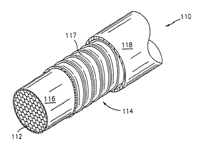
[0050] Referring now to FIG. 4 in detail, reference numeral I10 has been used
to
generally designate a more preferred embodiment of the insulated electrical
conductor of the
present invention. In this more preferred embodiment, insulated electrical
conductor 110
demonstrates improved flexibility, and comprises an electrical conductor 112,
which is
insulated with a multi-layer insulation system 114 comprising:
9
CA 02444044 2003-10-14
WO 02/084674 PCT/US02/12113
(1) a fluoropolymer inner layer 116,
wherein the fluoropolymer inner layer 116 is formed by either extruding a
fluoropolymer material along a portion or length of the electrical conductor
112, or wrapping
a fluoropolymer film, in an overlapping fashion, along the length of the
conductor 112,
(2) a polyimide film middle layer 117, wherein the polyimide middle layer
117 is formed by wrapping an optionally coated polyimide film, in an
overlapping fashion,
along a portion or length of the inner layer 116; and
(3) an extruded, crosslinked fluoropolymer outer layer 118.
[0051] Fluoropolymers which may advantageously be utilized in the inner layer
116
of the insulated electrical conductor 110 of the present invention include,
for example, MFA,
PFA, PTFE, ethylene-chlorotrifluoroethylene (ECTFE) copolymers, ethylene-
tetrafluoroethylene (ETFE) copolymers, polyvinylidene fluoride (PVDF),
tetrafluoroethylene-hexafluoropropylene-vinylidene fluoride (THV),
polyvinylfluoride (PVF)
resins, and mixtures thereof.
[0052] In a preferred embodiment, inner layer 116 is extruded and the
fluoropolymer
comprises a copolymer or terpolymer of ETFE. In a more preferred embodiment,
the
polymer is an ETFE terpolymer that has been compounded with a TAIC
crosslinking agent.
Such polymers are available from DuPont and Daikin, under the product
designations
TEFZEL HT200 fluoropolymer resin and NEOFLON EP-541 fluoropolymer resin,
2o respectively.
[0053] In yet a more preferred embodiment, inner layer 116 is extruded and
crosslinked and the extruded fluoropolymer material of inner layer 116 is
substantially the
same as the material used to prepare outer layer 118, but contains less
crosslinking agent.
[0054] In another preferred embodiment, inner layer 116 is wrapped and the
fluoropolymer is PTFE tape. In a more preferred embodiment, the PTFE is in the
form of a
skived tape, with such tapes being available from Goodrich Corporation, Four
Coliseum
Centre, 2730 West Tyvola Road, Charlotte, NC 28217-4578, under the product
designation
PTFE Skived Tapes.
[0055] The fluoropolymer film inner layer 116 may be a heat-sealed or a non-
heat-
sealed fluoropolymer film inner layer. It is noted that wrapped fluoropolymer
tapes or films
will fuse or bond to themselves in overlapping regions at temperatures at or
above the
CA 02444044 2003-10-14
WO 02/084674 PCT/US02/12113
melting point of the fluoropolymer, thereby obviating the need to employ a
heat-sealable
adhesive with such films.
[0056] The polyimide film of middle layer 117 is preferably applied to inner
layer
116 in tape form, by spirally wrapping the tape about inner layer 116, so as
to achieve a
degree of overlap ranging from about 10 to about 70 %. In one embodiment, the
polyimide
film of middle layer 117 does not employ a heat-sealable adhesive and is not
heat-sealed. In
another embodiment, the polyimide film employs a heat-sealable adhesive and is
substantially uniformly sealed to itself-in over-lapping regions along the
length of inner layer
116. In one such embodiment, inner layer 116 is formed using a fluoropolymer
tape and the
1o fluoropolymer tape is heated together with the coated polyimide film, but
is not sealed.
[0057] Preferred non-heat-sealable polyimide films have a thickness ranging
from
about 0.01 to about 0.04 mm, and are available from DuPont, under the trade
designation
KAPTON H and KAPTON E polyimide films. Preferred heat-sealable polyimide films
are
the same as those noted above for inner layer 16.
[0058] The preferred insulated electrical conductor 110 described above, which
employs a non-heat-sealed polyimide film middle layer, demonstrates a degree
of flex which
is substantially greater than prior art wire constructions. The degree of flex
or wire flexibility
is measured by: selecting a 0.9 meter section of insulated wire (i.e., an
insulated stranded
nickel plated copper conductor (20 American Wire Gage (AWG), 19 Strand, nickel
plated
copper) measuring 0.95 mm in diameter), which is substantially free of kinks
and bends;
attaching a ring connector to each end of the conductor; attaching a 100 gram
weight to each
ring connector; carefully suspending the insulated wire on a stationary
mandrel having a
diameter measuring 0.48 cm; waiting one minute; and measuring the width
between parallel
insulated wire segments at three different points along the length of the
wire. The degree of
flex or wire flexibility is an average of the three width measurements.
[0059] In a most preferred embodiment, insulated electrical conductor 110
comprises
an electrical conductor 112, which is insulated with a multi-layer insulation
system 114
comprising: (1) an extruded, crosslinked ETFE inner layer 116; (2) a non-heat-
sealed
polyimide film middle layer 117; and (3) an extruded, crosslinked ETFE outer
layer 118.
[0060] In another most preferred embodiment, insulated electrical conductor
110
comprises an electrical conductor 112, which is insulated with a multi-layer
insulation system
11
CA 02444044 2003-10-14
WO 02/084674 PCT/US02/12113
114 comprising: (1) a non-heat-sealed PTFE inner layer 116; (2) a heat-sealed
polyimide
film middle layer 117; and (3) an extruded, crosslinked ETFE outer layer 118.
[0061] It is noted that although the present inventive insulated electrical
conductor 10,
110 has been described hereinabove as an insulated stranded cable, it is not
so limited. The
insulated conductor 10, 110 may comprise a single wire covered with the multi-
layer
insulation system 14, 114 of the present invention, or may comprise a
plurality of bunched,
twisted, or bundled wires, with each wire separately covered with the multi-
layer insulation
system 14, 114. The insulated conductor 10, 110 may also comprise a plurality
of single or
dual layer insulated wires which are coated with the polyimide or
fluoropolymer inner layer
lo 16, 116 and optionally, with the polyimide film middle layer 117. In this
embodiment, the
plurality of single or dual layer insulated wires are covered with a sheath
consisting of the
crosslinked fluoropolymer outer layer 18, 118.
[00621 The process for preparing the insulated electrical conductor 10, 110 of
the
present invention basically comprises:
(a) forming a polyimide or fluoropolymer inner layer 16, 116 on an
electrical conductor 12, 112,
wherein, when the inner layer is a polyimide inner layer, the layer 16, 116 is
formed by wrapping a polyimide film, which has been coated with a sealable
component, in
an overlapping fashion, along a portion or length of the electrical conductor
12, 112, wherein
the sealable component comprises a perfluoropolymer, a crosslinked
fluoropolymer, or a
polyimide adhesive,
wherein, when the inner layer is a fluoropolymer inner layer, the layer 16,
116
is formed by either: i) extruding a fluoropolymer material along a portion or
length of the
electrical conductor 12, 112, or ii) wrapping a fluoropolymer film, in an
overlapping fashion,
along a portion or length of the electrical conductor 12, 112,
(b) optionally, forming a polyimide middle layer 117 on the polyimide or
fluoropolymer inner layer 16, 116 by wrapping an optionally coated polyimide
film, in an
overlapping fashion, along a portion or length of the inner layer 16, 116,
(c) when the inner layer 16, 116 is a polyimide inner layer or when a
middle layer 117 is formed using a coated polyimide film, heating the
polyimide film or films
to a temperature ranging from about 240 to about 350 C to cause overlapping
regions of the
12
CA 02444044 2006-09-06
coated film or films to bond, thereby forming an effective seal against
moisture along the
length of the conductor 12, 112,
(d) forming a fluoropolymer outer layer 18, 118 on either the inner or
middle layer 16, 116, 117 by extruding a fluoropolymer material along a
portion or length of
that layer; and
(e) crosslinking the fluoropolymer outer layer 18, 118, wherein, when the
inner layer 16, 116 or the sealable component comprises a perfluoropolymer
(e.g.,
polytetrafluoroethylene, fluorinated ethylene propylene copolymers,
perfluoroalkoxy resins),
the fluoropolymer outer layer 18, 118 is crosslinked by exposing it to less
than 60 megarads
to of radiation, with applied voltages ranging from about 50 to about 120 kilo
volts,
wherein, when the inner layer 16, 116 is a fluoropolymer inner layer, the
process for preparing an insulated, electrical conductor includes forming a
polyimide middle
layer 117 on the polyimide or fluoropolymer inner layer 16, 116.
(00631 Insulated electrical conductors 10, 110 that do not employ
perfluoropolymers
are preferably subjected to an irradiation step to effect crosslinking in the
fluoropolymer
outer layer 18, 118. In a more preferred embodiment, the dosage of ionizing
radiation (e.g.,
accelerated electrons or gamma rays) employed in the irradiation step is below
50 megarads
(Mrads), more preferably, between 5 and 25 Mrads and, most preferably, between
15 and 25
Mrads, while applied voltages range from about 0.25 to about 3.0 mega volts
(MV), and
preferably range from about 0.5 to about 1.0 MV. The irradiation step is
preferably carried
out at ambient temperature.
[0064] Insulated electrical conductors 10, 110, which employ an inner layer or
sealable component comprising a perfluoropolymer are subjected to a so-called
"skin
irradiation" process to effect crosslinking in the fluoropolymer outer layer
18, 118. The
subject process employs ionizing radiation in the form of accelerated
electrons, and basically
comprises using an accelerated voltage such that the maximum attained distance
of
accelerated charged particles is less than or equal to the thickness of the
outer layer 18, 118.
More specifically, with an applied voltage of 120 KV, most electrons will
penetrate outer
layer 18, 118 to a maximum depth of approximately 0.13 mm.
[0065J Such a technique or process is briefly described in JP 4-52570 in
regard to
automotive low voltage wire coated with e.g. a soft vinyl chloride resin.
13
CA 02444044 2003-10-14
WO 02/084674 PCT/US02/12113
[0066] In a preferred embodiment, the dosage of ionizing radiation (f.e.,
accelerated
electrons) employed in the irradiation step is below 60 Mrads, more
preferably, between 20
and 50 Mrads and, most preferably, between 30 and 40 Mrads, while applied
voltages range
from about 50 to about 120 kilo volts (KV), and preferably range from about
100 to about
120 KV. The "skin irradiation" technique or process is preferably carried out
at ambient
temperature.
[0067] It is noted that in the "skin irradiation" technique described above,
where
electrons do not reach the conductor during electron beam irradiation,
electrons may
accumulate in the insulation thereby increasing the possibility of flooding
and/or channeling.
lo As will be readily appreciated by those skilled in the art, electron
flooding and channeling
may damage the insulation by causing the formation of tiny pin-holes.
[0068] The present inventors have discovered that by exposing "skin
irradiated"
insulated electrical conductor 10, 110 to elevated temperatures ranging from
about 150 to
about 220 C, accumulated electrons may be more effectively drained off
without damaging
the insulation.
[0069] The insulated electrical conductor 10, 110 of the present invention is
lightweight, and may be used in environments where temperatures may exceed 230
C. Ih
addition, the inventive conductor 10, 110 demonstrates mechanical durability
and resistance
to hydrolysis.
[0070] Preferably, insulated conductor 10, 110 weighs from about 1.9 to about
2.0
kilograms (kg) per 305 meters (m), which serves to satisfy the maximum weight
limits set
forth in the following Military Specifications - M22759/92-20, M22759/86-20,
M22759/32-
20, and M22759/34-20.
[0071] The 230 C temperature rating of insulated electrical conductor 10, 110
was
determined in accordance with Military Specification MIL-DTL-22759/87A -
Accelerated
Aging Test. This test, which requires aging wire samples for 500 hours in an
air-circulating
oven maintained at a temperature of 290 C, was modified to the extent that the
oven
temperature was reduced to 260 C.
[0072] Mechanical durability is evidenced by the ability of insulated
electrical
conductor 10, 110 to pass the following tests: (1) Wire-to-Wire Abrasion
Resistance - Boeing
Specification Support Standard BSS 7324 entitled "Procedure for Testing
Electrical Wire and
Cable" dated December 2, 1998 ("Boeing BSS 7324); (2) Dynamic Cut-Through
Resistance
14
CA 02444044 2003-10-14
WO 02/084674 PCT/US02/12113
(at elevated temperatures of up to 260 C) - ASTM D 3032, Section 22, and
Military
Specification MIL-DTL-22759/87A; and (3) Sandpaper Abrasion Resistance -
Society of
Automotive Engineers (SAE) test method J 1128 Section 5.10.
[0073] The resistance to hydrolysis demonstrated by insulated electrical
conductor 10,
110 was measured in accordance with SAE test method AS4373, Section 4.6.2,
Method 602.
[0074] In a more preferred embodiment, the multi-layer insulation system and
insulated electrical conductor 10, 100 of the present invention demonstrate
other desirable
properties including excellent resistance to flame, the ability to be marked
using ultraviolet or
visible radiation, electrical resistance, humidity resistance, low smoke
generation, notch
propagation resistance, weathering resistance, wet and dry arc track
resistance, and resistance
to common solvents and other fluids used in the aircraft industry.
[0075] The subject invention will now be described by reference to the
following
illustrative examples. The examples are not, however, intended to limit the
generally broad
scope of the present invention.
WORKING EXAMPLES
Components Used
[0076] In the Working Examples set forth below, the following components and
materials were used:
CONDUCTOR: a stranded nickel plated copper conductor (20 American
Wire Gage (AWG), 19 Strand, nickel plated copper)
measuring 0.95 mm in diameter.
POLYIMIDE
FILM I: heat-sealable polyimide film coated or laminated on both
sides with a heat-activated, high temperature polyimide
adhesive, marketed under the trade designation KAPTON
HKJ heat-sealable polyimide film, by DuPont.
POLYIMIDE
FILM II: heat-sealable polyimide film coated or laminated on both
sides with a heat-activated, high temperature polyimide
adhesive, marketed under the trade designation KAPTON
EKJ heat-sealable polyimide film, by DuPont.
CA 02444044 2003-10-14
WO 02/084674 PCT/US02/12113
POLYIMIDE
FILM III: heat-sealable polyimide film coated or laminated on both
sides with a heat-activated, medium temperature polyimide
adhesive, marketed under the trade designation KAPTON
ELJ heat-sealable polyimide film, by DuPont.
POLYIMIDE
FILM IV: heat-sealable polyimide film coated or laminated on both
sides with a heat-activated perfluoropolymer adhesive,
marketed under the trade designation KAPTON XP heat-
sealable polyimide film, by DuPont.
POLYIMIDE
FILM V: heat-sealable polyimide film coated or laminated on both
sides with a heat-activated perfluoropolymer adhesive,
marketed under the trade designation OASIS TWT561 heat-
sealable polyimide film, by DuPont.
ETFE: a copolymer comprising 35 to 60 mole % of ethylene; 60 to
35 mole % of tetrafluoroethylene; and up to 10 mole % of a
fluorinated termonomer, marketed under the trade
designation TEFZEL HT 200 fluoropolymer resin, by
DuPont. Melting point of fluoropolymer resin is
approximately 270 C.
ETFE(I): a copolymer comprising 30 to 50 mole % of ethylene; 70 to
50 mole % of tetrafluoroethylene; and up to 10 mole % of a
fluorinated termonomer, marketed under the trade
designation TEFZEL HT 2127 fluoropolymer resin, by
DuPont. Melting point of fluoropolymer resin is
approximately 243 C.
PTFE: a skived polytetrafluoroethylene film, marketed under the
trade designation TEFLON TFE fluoropolymer resin, by
DuPont.
TAIC: a triallyl isocyanurate crosslinking agent, marketed under the
designation TAIC triallyl isocyanurate, by Nippon Kasei
Chemical Co., Ltd., Tokyo, Japan.
Ti02: titanium dioxide pigment in powder form (z96 % in purity),
marketed under the trade designation TIPURE titanium
dioxide pigment, by DuPont.
16
CA 02444044 2003-10-14
WO 02/084674 PCT/US02/12113
Sample Preparation
Examples IA to JE
[0077] A continuous strip of POLYIMIDE FILM I, measuring 0.64 cm in width and
0.03 mm in thickness, was spiral-wrapped, at a 53 % overlap, about a
CONDUCTOR. The
spiral-wrapped CONDUCTOR was then heated in a continuous process to a
temperature in
excess of 300 C for approximately 5 seconds to heat-seal the overlapping
portions of the
POLYIMIDE FILM I strip, and was then allowed to cool. The thickness of the
heat-sealed,
spiral-wrapped POLYIMIDE FILM I inner layer was 0.05 mm.
[0078] A quantity of ETFE was compounded with 8 % by wt. TAIC and 2 % by wt.
to TiO2 and was then extruded over the POLYIMIDE FILM I inner layer using a
single-screw
extruder having four heating zones which were set at 200 , 240 , 275 , and 290
C,
respectively. The thickness of the extruded ETFE layer was 0.13 mm.
[0079] Test samples were then irradiated using electron-beam radiation, with
air-
cooling. Total beam dosages were 10, 15, 20, or 30 megarads, while applied
voltages were
either 120 KV, 150 KV, or 0.5 MEV.
[0080] The subject wire construction is described in Table 1, hereinbelow.
Examples 2, 3A to 3C, 4A and 4B
[0081] Four test samples of the wire construction labeled Example 2, ten test
samples
of Example 3, and six test samples of Example 4, were prepared substantially
in accordance
with the method identified above for Example 1, except that test samples for
each Example
were prepared using a different polyimide film. As above, total beam dosages
were 10, 15,
20, or 30 megarads, while applied voltages were either 120 KV, 150 KV, or 0.5
MEV.
[0082] The subject wire constructions are more fully described in Table 1,
hereinbelow.
Exaniple 5
[0083] One thousand feet of the wire construction labeled Example 5 were
repared
substantially in accordance with the method identified above for Examples IA
to IE, except
that total beam dosage was 18 megarads, while applied voltages were 0.5 mega
electron
volts.
100841 The subject wire construction is more fully described in Table 1,
hereinbelow.
17
CA 02444044 2003-10-14
WO 02/084674 PCT/US02/12113
Exaniples 6 to 9
[0085] A continuous strip of PTFE, measuring 0.63 cm in width and 0.025 mm in
thickness, was spiral-wrapped, at either a 54 % overlap (Example 6) or a 15 %
overlap
(Examples 7 to 9), about a CONDUCTOR. A continuous strip of either POLYIMIDE
FILM
III (Examples 6 and 7), measuring 0.63 cm in width and 0.025 mm in thickness
or
POLYIMIDE FILM II (Examples 8 and 9), measuring 0.63 cm in width and 0.018 mm
in
thickness, was then spiral-wrapped, at a 54 % overlap, about the spiral-
wrapped PTFE inner
layer. The spiral-wrapped CONDUCTOR was then heated in a continuous process to
a
temperature in excess of 300 C for approximately 5 seconds to heat-seal the
overlapping
l o portions of the POLYIMIDE FILM layer, and was then allowed to cool. The
thickness of the
inner and middle layers was 0.076 mm (Examples 6 and 7) and 0.061 mm (Examples
8 and
9).
[0086] A quantity of ETFE or ETFE(I) was compounded with 8 % by wt. TAIC and 2
% by wt. TiO2 and was then extruded over the POLYIMIDE FILM middle layer using
a
single-screw extruder having four heating zones which were set at 200 , 240 ,
275 , and
290 C, respectively. The thickness of the extruded ETFE or ETFE(I) layers was
0.13 mm
(Examples 6 and 7) and 0.14 mm (Examples 8 and 9).
[0087] Five hundred feet of each test sample wire construction were then
irradiated
using electron-beam radiation, with air-cooling. Total beam dosages were 18
megarads for
Examples 6 and 7, and 36 megarads for Examples 8 and 9, while applied voltages
were 0.5
MEV.
[0088] The subject wire constructions are more fully described in Table 1,
hereinbelow.
Examples C-1 and C-2
[0089] Four test samples each of prior art wire constructions C-1 and C-2 were
prepared as set forth below.
[0090] C-1 was prepared substantially in accordance with the method identified
above
for Example 1, except that 0.06 mm thick PTFE tape was spiral-wrapped, with a
53 %
overlap, over a spiral-wrapped POLYIMIDE FILM IV inner layer prior to heat-
sealing. The
resulting wire construction was then exposed to a temperature in excess of 330
C to effect
heat-sealing in both layers.
18
CA 02444044 2003-10-14
WO 02/084674 PCT/US02/12113
[0091] C-2 was prepared by compounding ETFE with 1.5 % by wt. TAIC, and then
by extruding the compounded material over the CONDUCTOR using a single-screw
extruder, as described above. A quantity of compounded ETFE material, which
had been
compounded with 8 % by wt. TAIC, was then extruded over the ETFE inner layer,
and the
resulting wire construction irradiated using electron-beam radiation, with air
cooling. Total
beam dosage was 30 megarads, with an applied voltage of 0.5 MEV.
[0092] The subject prior art wire constructions are more fully described in
Table 1,
hereinbelow.
19
CA 02444044 2003-10-14
WO 02/084674 PCT/US02/12113
N W a ! W 0
U 2 o S o
N o0
U > r- uõ o nF o d ~c
ou.
~ ti E O ly O fs" N t~
O C ~O
O V+
v '.
N ,o W o E~ a o w = N v
u.
F O ?~-' O O O
..~ ' Lt'
Q
~C
c~
u o
w N
p r, EtJ p E 0. wõ N
0. 'T-_ p w C O 10
kn 0.OCi.
=d=
o E E 0. o w M F =T ~. 1"O O ~O
-, p a O aL"
M
Q N
I W
otn E~ a i ~ ~ IFy o o
o
Q a
x d,
Gy IM E a o w ~ ry v
p v ow
V M
! w s
cn TE 0' oo ~ { H o o ~ o
w =;, ~
E
'Cp T
0 p
U 06
N =T ~ 0.' O ~ ~ i C N R
~1,õ o ,O II '
a a
V W b f W
~ q > w a o i ~ ~ 1 o o
Q a
~ o~ o o v 'oon'o
N y ~ y y =C N =~ f0
ttl >d
a'~ ~ N =~ C N ~ ...1 C "'~ ~ C _ ~ ~ E
"~o=E~ oy'e~ oc 'E
Q F - ~ ~.a Q F~.1 O FO ~ F~F E F o3 ~
V1 ~ ~ N N cn
CA 02444044 2006-09-06
[0093) The prepared test samples were then subjected to the test procedures
identified
below. Test procedures, with the exception of ease of peel, are fully
described in the
following publications: (1) Boeing Specification Support Standard BSS 7324
entitled
"Procedure for Testing Electrical Wire and Cable" dated December 2, 1998
("Boeing BSS
7324"); (2) Military Specification MIL-DTL-22759/87A entitled "Wire,
Electrical,
Polytetrafluoroethylene/Polyimide lnsulated, Normal Weight, Nickel Coated
Copper
Conductor, 260 C, 600 Volts," and dated February 23, 1998; (3) Military
Specification
MIL-STD-2223 entitled "Test Methods for Insulated Electrical Wire," and dated
August 31,
1992; (4) Society of Automotive Engineers (SAE) test method AS4374 entitled
"Test
to Methods for Insulated Electrical Wire," and dated August, 1994; and (5) SAE
test method
J 1128 entitled "Surface Vehicle Standard, Low Tension Primary Cable," and
dated May,
2000.
Test Methods
Accelerated Aging or
Shrinkage Resistance (P,F): Boeing BSS 7324, paragraph no. 7.1 a, pp. 12 to
14, conducted
at 280 C.
Current Overload
Capacity: Boeing BSS 7324, paragraph no. 7.16, pp. 48 to 50, conducted
at room temperature.
The insulated wire test samples were evaluated for current
overload capacity by removing 13mm of insulation from wire
samples measuring 1.5m in length. The samples were then
suspended horizontally in a test set-up with no visible sag.
Then, 33 amperes (amps) of current was applied to each test
sample for a period of 5 minutes and the samples cooled to
room temperature. Each test sample was visually inspected
during current application and after the samples were retumed
to room temperature. The test samples were then subjected to
the dry dielectric test that is described in the Boeing BSS 7324
Specification. The test, which was repeated six times, was
deemed passed if at least five out of the six samples passed the
test.
Cut-Through
Resistance (lbs): MIL-DTL-22759/87
Boeing BSS 7324, paragraph no. 7.23, p. 58, Dynamic Cut-
Through
21
CA 02444044 2003-10-14
WO 02/084674 PCT/US02/12113
The insulated wire samples were tested for cut-through
resistance using the method described below. The cut-through
test measured the resistance of the wire insulation to the
penetration of a cutting surface and simulated the type of
damage that can occur when a wire is forced by mechanical
loading against a sharp edge. The test was performed at room
temperature (23 C), at 150 C, at 200 C, and at 260 C, to
evaluate the effect of the elevated temperature on insulation
performance. The standard cutting edge used was stainless steel
and had a radius of 0.406 mm.
For each test, a 600 mm (in length) test sample was clamped in
place between a blade and a flat plate within an INSTRON
is compression tester, and the ends of the conductor connected to
an 18 VDC electrical circuit. The cutting edge of the blade was
oriented perpendicularly to the axis of the sample. The cutting
edge was then forced through the insulation at a constant rate of
1.27 mm per minute until contact with the conductor occurred.
A detection circuit sensed contact of the cutting edge with the
conductor and recorded the maximum force, encountered during
the test. The test was then repeated four times rotating the
sample between tests to offset the effect of eccentric insulation.
The reported cut-through resistance was the arithmetic mean of
five tests performed on each sample.
Dry Arc Propagation
Resistance (P,F, or
number of wires passed): MIL-STD-2223 Method 3007.
Boeing BSS 7324, paragraph no. 7.4, pp. 16 to 30, conducted at
room temperature.
The insulated wire samples were tested for dry arc propagation
resistance using the method described below. Each test sample
was cut into 7 pieces, with each piece measuring 35 cm in
length. The insulation from five of the seven pieces was
stripped from the ends of each piece exposing about 5mm of
conductor and the pieces designated "active wires." The
insulation from the remaining two wires was left intact and the
pieces designated "passive wires."
The seven wire pieces were then bundled such that one active
wire was located in the center of the bundle while the
remaining six wire pieces surrounded the central active wire.
The two passive wires were located side-by-side within the
bundle. The seven-wire bundle was laced together at four
locations so as to keep all seven wires tightly held together
22
CA 02444044 2003-10-14
WO 02/084674
PCT/US02/12113
throughout the length of the bundle. The distance between the
two central laces was about 2.5 cm, while the distance between
the central two laces and the outer two laces was about 1,25
cm.
The wire bundle was then placed in a jig similar to that shown
in the Boeing BSS 7324 Specification. The two passive wires
were located at the bottom of the jig, while the stripped wires
were individually connected to an electrical circuit. More
specifically, the five active wires were connected to a three
phase 400 Hz power source. Then, a knife blade with a 250 gm
load was placed on top of the wire bundle perpendicular to
each wire and the blade movement initiated. The blade moved
back and forth at a speed of 0.75 cycles/second. When the top
two wires were shorted out, the system was de-energized. Each
wire was exposed to a 1000 volt wet dielectric withstand test to
check whether the remaining insulation could withstand such
voltage. When the insulation withstood 1000 volts, the voltage
was increased to 2500 volts. When the wire withstood 1000
volts, it is considered to have passed the test.
This test was deemed passed if: (1) a minimum of 64 wires
passed the dielectric test; (2) three wires or less failed the
dielectric test in any one bundle; and (3) actual damage to the
wire was not more than 3 inches in any test bundle.
Ease of Peel: Test samples employing a dual layer insulation system and
measuring 0.9 meter in length were tested for ease of peel by
(1) removing the outer insulation layer, (2) manually seizing a
leading edge of the inner insulation layer (i.e., polyimide tape),
and (3) slowly peeling the tape off of the conductor or wire.
The inner insulation layer was deemed "continuously peelable"
if the entire width of the tape could be continuously peeled
from at least five revolutions of the wire without tearing.
Hydrolysis Resistance (P,F): MIL-DTL-22759/87A and SAE AS4373, Method 602 Test
(Unconditioned Wire: AS4373, Section 4.6.2.4.2)
Test samples having an insulation thickness of approximately
0.20 mm and measuring approximately 762 mm in length were
separately fixed and wound on an 8 mm mandrel and placed in
salt solution [5% (m/m) of NaCI in water] contained in a 2 liter
beaker. The ends of each wound test sample were positioned
outside or above the salt solution in the beaker. The test
samples were then allowed to age in the salt solution for from
672 to >10,000 hours at 70 C 2 C. Starting at 672 hours, the
test samples were visually inspected and then periodically
subjected to the Withstand Voltage Test as described below.
23
CA 02444044 2003-10-14
WO 02/084674 PCT/US02/12113
The Hydrolysis Test was deemed "passed" if the sample, upon
being subjected to the Withstand Voltage Test, did not
demonstrate any electrical breakdown.
Withstand Voltage Test (P,F): For this test, the ends of each
test sample were twisted together to form a loop. The looped
test sample was then immersed in the salt solution contained in
the beaker. The ends of each test sample were located above
the solution. A test voltage of 2.5 kV (rms) was then applied
through an electrode between the conductor and the solution for
five (5) minutes.
Life Cycle (P,F): MIL-DTL-22759/87A. Five (5) hours at 230 to 290 C 2 C.
Dielectric test, 2.5 kV (rms) for five (5) minutes.
Test samples were tested for life cycle by aging the samples
and then by subjecting the aged samples to the Withstand
Voltage Test noted above. The samples were aged by
separately fixing the samples on a mandrel having a one-half
inch diameter and then placing the mandrel and test samples in
an air circulation oven set at 30 C above the intended
temperature rating for the product, for a period of 500 hours.
Laser Markability: Boeing BSS 7324, paragraph no. 7.36, pp. 82 to 83,
conducted
at room temperature.
Test conducted by Spectrum Technologies PLC, Western
Avenue, Bridgend CF31 3RT, UK, using a CMS 11 Contrast
Meter.
Sandpaper Abrasion (mm): SAE J1128, Section 6.10
Test samples having an insulation thickness of approximately
0.20mm and measuring 1,000mm in length were tested for
sandpaper abrasion resistance by removing 25mm of insulation
from one end of each test sample and by horizontally mounting
each test sample (taut and without stretching) on a continuous
strip of abrasion tape in an apparatus that was built by Glowe-
Smith Industrial, Inc. (G.S.I. Model No. CAT-3) in accordance
with Military Specification MIL-T-5438 and that was capable
of exerting a force on the sample while drawing the abrasion
tape under the sample at a fixed rate. For each test, 150J garnet
sandpaper (with 10mm conductive strips perpendicular to the
edge of the sandpaper spaced a maximum of every 75mm) was
drawn under the sample at a rate of 1500 75mm/min while a
total force of 2.16 0.05 N was exerted on the test sample.
The sandpaper approached and exited each test sample from
24
CA 02444044 2003-10-14
WO 02/084674 PCT/US02/12113
below at an angle of 29 2 to the axis of the test sample and
was supported by a rod 6.9mm in diameter. The length of
sandpaper necessary to expose the core or wire was recorded
and the test sample moved approximately 50mm and rotated
clockwise 90 . The above-referenced procedure was repeated
for a total of four readings. The mean of the four readings
constituted the sandpaper abrasion resistance for the subject test
sample.
It is noted that since the test samples had very thin insulation,
this test had to be stopped frequently to observe failure points.
Strippability: ASTM D3032 Section 27.
Boeing BSS 7324, paragraph no. 7.48, pp. 96 to 97, conducted
at room temperature.
Test samples were tested for strippability by carefully removing
70mm of insulation from test samples measuring 76mm in
length. The bare conductor portion of the test specimen was
then threaded through a loosely fitted hole of a jig so that the
unstripped insulation stayed at one side of the jig and the
stripped wire at the other. Using an INSTRON Tensile Tester,
the bare conductor was pulled while the jig was fixed in place.
The force required to pull the remaining 6mm slug of insulation
from the test sample was reported as strip force.
This test was deemed passed if the strip force fell within the
range of from 1/4 to 6 pounds (lbs).
Wet Arc Propagation
Resistance (P,F, or
number of wires passed): MIL-STD-2223, Method 3006.
Boeing BSS 7324, paragraph no. 7.4.6 & 7, pp. 26 to 29,
conducted at room temperature
Test samples were tested for wet arc propagation resistance by
preparing seven test samples measuring 35cm in length from a
3m long insulated wire sample. Five of the seven wire
segments were stripped at both ends exposing about 5mm of
conductor. These stripped wire segments were designated
"active wires." The remaining two wire segments that were not
stripped were called "passive wires."
The seven wire pieces were then bundled such that one active
wire was located in the center of the bundle while the
remaining six wire pieces surrounded the central active wire.
CA 02444044 2003-10-14
WO 02/084674 PCT/US02/12113
The two passive wires were located side-by-side within the
bundle. The seven-wire bundle was laced together at four
locations so as to keep all seven wires tightly held together
throughout the length of the bundle. The distance between the
two central laces was about 2.5 cm, while the distance between
the central two laces and the outer two laces was about 1.25
cm.
Two wires located on top of the seven-wire bundle had slits
measuring 0.5 to 1.0mm in width that were perpendicular to the
wire axis. The slits were positioned 6mm apart. The stripped
wires were connected to a three phase power source according
to the scheme set forth in the Boeing BSS 73244 Specification.
The wire bundle was energized and a 5% aqueous salt solution
was dripped onto the wire bundle where the two exposed slits
were located. The rate of application of the salt solution was 8
to 10 drops per minute. This condition was continued for 8
hours unless the bundle failed by tripping a circuit breaker.
After an 8-hour exposure to the dripping salt solution under the
energized condition, the wire bundles were taken out. Each
wire was initially exposed to a 1000 volt wet dielectric
withstand test initially, then 2500 volts. When a wire
withstood a 1000 volt wet dielectric withstand test, it passed
the test.
This test was deemed passed if: (1) a minimum of 64 wires
passed the dielectric test; (2) three wires or less failed the
dielectric test in any one bundle; and (3) actual damage to the
wire was not more than 3 inches in any test bundle.
Wire-to-wire abrasion
resistance (cycles to failure,
6,150,000 cycles minimum): Boeing BSS 7324, paragraph no. 7.57, p. 108.
Test samples were tested for wire-to-wire abrasion resistance in
accordance with the following method. One wire test sample
measuring approximately 28cm in length was crossed with
another wire sample measuring approximately 40cm in length
at the center of the shorter wire as shown in the Boeing BSS
7324 Specification. One end of one wire specimen was fixed
on an upper plate while the other end of the same wire was
fixed on a lower plate. One end of the other wire was fixed on
the lower plate while the other end of the same wire was loaded
with a 1.13 Kg weight. The upper and lower plates were 45mm
apart.
26
CA 02444044 2003-10-14
WO 02/084674 PCT/US02/12113
The lower plate moved back and forth with a 6.35mm double
amplitude at 10 cycles per second. The fixed member of the
wire was connected to a power source so that the cycle counter
stopped when the two wire specimens made an electrical
contact by wearing out the insulation layer. If the cycle count at
the stopping point was greater than 6,150,000, the result was
considered passing.
Working Example 1A
[0094] In this example, the prepared wire constructions or test samples were
tested
for shrinkage resistance, mechanical durability, hydrolysis resistance, and
wet arc track
resistance, while confirming the temperature rating of 230 C. The results are
set forth in
Table 2, hereinbelow.
TABLE 2
Summary of Example ]A
EXAMPLE TOTAL ELECTRON LIFE ACCELERATED HYDROLYSIS WETARC WIRE-TO-WIRE
BEAM BEAM CYCLE AGING RESISTANCE' PROPAGATION ABRASION
DOSAGE VOLTAGE (P,F) (P,F) (P,F) RESISTANCE (6,150,000 cycles
(Mrad) (MV) (P,F) minimum)
1A 30 0.5 P P P p 42,885,600
1 2000 hour requirement met, test continuing.
[0095] As shown in Table 2, the insulated conductor of the present invention
may be
used at temperatures of up to 230 C, and demonstrates a balance of properties
including
shrinkage resistance, mechanical durability, hydrolysis resistance, and wet
arc propagation
resistance.
27
CA 02444044 2003-10-14
WO 02/084674 PCT/US02/12113
Working Examples 1B, 2, 3A, C-I and C-2
[0096] In these examples, the prepared wire constructions or test samples were
tested
for sandpaper abrasion resistance. The results are reported in Table 3,
hereinbelow.
TABLE 3
Summary of Examples 1 B, 2, 3A, C-1 and C-2
EXAMPLE TOTAL ELECTRON SANDPAPER ABRASION (mm)
BEAM BEAM
DOSAGE VOLTAGE (MV)
Mrad
OUTER LAYER AVG. BOTH LAYERS AVG.
1B 30 0.5 40 42 117 124
14 153
41 151
46 75
2 30 0.5 38 43 229 172
41 158
43 153
48 146
3A 30 0.5 37 41 114 142
40 148
41 153
46 151
C-1 N/A N/A 9 12 117 109
11 153
13 79
16 85
C-2 30 0.5 40 53 164 157
53 151
56 153
62 158
100971 As shown by Examples 1B, 2, and 3A in Table 3, the insulated conductor
of
the present invention demonstrated a resistance to sandpaper abrasion which
was greatly
improved over that demonstrated by the prior art wire construction Example C-
1, which
employed a PTFE outer layer.
28
CA 02444044 2003-10-14
WO 02/084674 PCT/US02/12113
Working Examples IC, 1D, 1E, 3B, 3C, 4A and 4B
[0098] In these examples, the prepared wire constructions or test samples were
tested
for ease of peel. The results are shown in Table 4, hereinbelow.
TABLE 4
Summary of Examples 1 C, l D, 1 E,313, 3C, 4A and 4B
EXAMPLE TOTAL BEAM BEAM VOLTAGE EASE OF PEEL
DOSAGE (Mrad) (KV)
1 C 10 120 not continuously peelable
not continuously peelable
10 20 not continuously peelable
ID 10 150 not continuously peelable
15 not continuously peelable
not continuously peelable
lE 30 500 not continuously peelable
3B 10 120 not continuously peelable
15 not continuously peelable
15 20 not continuously peelable
3C 10 150 continuously peelable
15 continuously peelable
20 continuously peelable
4A 10 120 not continuously peelable
15 not continuously peelable
20 20 not continuously peelable
4B 10 150 continuously peelable
15 continuously peelable
20 continuously peelable
[0099] Examples 3B and 4A demonstrate that insulated conductors employing
irradiation degradable perfluoropolymer adhesives may be successfully prepared
using a
"skin irradiation" technique which effects crosslinking of the outer layer
using low electron
beam voltages of less than or equal to 120KV. As shown in Examples 3C and 4B,
exposing
these samples to electron voltages of 150KV appears to degrade the adhesive
resulting in a
sample where the outer layer is continuously peelable along the length of the
test sample.
[0100] Examples 1C, 1D and IE, which employed a polyimide adhesive, were not
easily peelable regardless of whether the sample was irradiated at 120, 150 or
500KV, which
indicated that higher electron beam voltages do not serve to degrade the
polyimide adhesive.
29
CA 02444044 2003-10-14
WO 02/084674 PCT/US02/12113
Working Examples 5 to 9, C-1 and C-2
[0101j In these examples, the prepared wire constructions or test samples were
tested
for hydrolysis, sandpaper abrasion, cut-through, wet and dry arc propagation
and wire-to-wire
abrasion resistance, laser markability, strippability, life cycle and current
overload capability.
The results are set forth in Table 5, hereinbelow.
CA 02444044 2003-10-14
WO 02/084674 PCT/US02/12113
~'I'D, 000
aa R
.9 N n f~ n ~ n h
in R Rt 3 ~
c 3 N
v ~ in in !~n ~n
ca t"" C N ~
tn~ C 7 ~
p
oa~
a 'o
0
Q~ .d 'Q Vl Vl Vl Vl Vl
O C~ O .~ 6
3 R
c v
d o~~ tn tn tn kn tn
C y
O
U '~ O ~ N N vl v1 ~ ~n V1 ~
~ tit C a ~ ~
+
:t.0 R
Cz: Oõ Q
Q 4A.. TJ V1 Vl vl 1 ~/1 vl v1
U 0 4, c a,~ - I
p~
kn O
kn U N M l~ O O b
'COV 10 10 ~' fV
V1 ~1 V1
1M=1 10 V
~ 'y N
Up O N O O N
~A C O V1 V~1 V~1 ~~
N
O
a U o~ o c, O O
O M N" I- i/1 V'1
C(~ n ~D V1 n ~O
11 10 O O
7 O~ ~/i O~ O T V' M
U N 00 rn o0 oa r-
_o 0
Q~ 3S
C N ~ T~ c~ V dN N1.~
v~a oa0
N u
5 a aao.,r,,,aa
v N
C
s
~ 1~ O b oo 00
O_ M M
N N~~ N N N a
E - r F~- E o 0 0 0 o c o ~
ou
c
o. ~
X ~ N O
tr~ ~n ~o t~ o0 0~ U U o
ti
~
tn o ~n
31
CA 02444044 2003-10-14
WO 02/084674 PCT/US02/12113
b~~
o=~ a a a a. a a a
o > m
UoU
a~
a
N M M M O M O M N M O M M
w
0
~
Ny
N Y
~ N
3 ~
p N M M M M M M M M M M M M
N 3
U
0
U
C w
.-. y
~U lc~
~ o ~ o 0 0 0 0 0 0 0 0 0 0 0
M"O M"O MI'O M~O M\O M 01
~ if) E-. N N N N N N N N N N N N
v (n
tnc
a cq3 Qo
~1W
0 0 0 0
C) o 00 0 0
ca o 'ai ' o0
U o
00 o t- 1 ~ tn
0 ~ oo ~O t~
N N A A
=~
y ~O M V=1 00 O~
M M
p M
=~ L
V] Vtap=
~~ u~ Q I 1 1 ~ ~ ~ 1
~l~zou
G N
p~ O O 00 00 O M M
= O ~ ON O\ - O O
N ~ N N N
7=- O O C O O O O
~
N
w tn ~o t- 00 a. U U
~n o ~n
32
CA 02444044 2003-10-14
WO 02/084674 PCT/US02/12113
[0102] As shown in 'Table 5, the insulated conductors of the present invention
demonstrate a balance of properties including mechanical durability and
hydrolysis
resistance. More specifically, Examples 5 to 7 demonstrated good hydrolysis
resistance, with
Examples 8 and 9 noted as currently being tested but expected to demonstrate
the same level
of resistance. With regard to sandpaper abrasion resistance, Examples 5 to 7
performed
similar to Comparative Example C-2. Examples 8 to 9 showed a slight drop-off
in this
property, while Comparative Example C-1 performed poorly presumably due to the
nature of
the PTFE outer layer. In terms of cut-through and wire-to-wire abrasion
resistance
properties, the insulated conductors of the present invention demonstrated
greatly improved
1o cut-through resistance over Comparative Examples C-1 and C-2, at all of the
temperatures
tested, while Examples 5, 7 and 8 demonstrated remarkable levels of wire-to-
wire abrasion
resistance. With regard to wet arc propagation resistance, Examples 6, 7 and 9
passed each
test, while Example 5 passed a majority of the tests. Similar results were
obtained for dry arc
propagation resistance, with each Example passing all, or a majority of, the
tests. In addition,
Examples 8 and 9 both demonstrated improved laser markability over Comparative
Example
C-1, while all of the inventive insulated conductors successfully passed the
industry standard
for strippability, namely - a strip force of from '/4 to 6 lbs. With regard to
life cycle and
temperature ratings, Example 8 qualified for a temperature rating of 230 C.
Finally, all of
the test samples satisfied the requirements for threshold current overload
capacity.
[0103] Although the present invention has been shown and described with
respect to
detailed embodiments thereof, it will be understood by those skilled in the
art that various
changes in form and detail thereof may be made without departing from the
spirit and scope
of the claimed invention.
101041 Having thus described the invention, what is claimed is:
33