Note: Descriptions are shown in the official language in which they were submitted.
CA 02444231 2003-10-24
NETWORK TERMINATION EQUIPMENT
BACKGROUND OF THE IN~7ENTIOI~T
1. Technical Field of the Invention
The present invention relates to providing high-
speed communications services to ordinary residences and
small businesses on digital subscriber lines.
~~ Background of the Invention
The sudden emergence of the Internet has produced an
urgent demand for high-speed communications services to
ordinary residences and small businesses. These services
are distinguished by bursty data patterns and
asymmetrical data transfer - far more information sent
toward the subscriber premises than received from it. A
partial response to this need, at least on the physical
signal level, has been found in new 'exDSLI° transmission
technologies, such as ADSL (Asymmetric Digital Subscriber
Line). These have recently become sophisticated enough
to allow dynamic bit-rate adaptation on each subscriber
line, so that a wide range of loop lengths can be
accommodated. But all this variability (bursty data,
dynamic bit rates, etc~) has made it nearly impossible to
predict, control, manage, or guarantee th.e Quality of
Service (QoS) provided to each subscriber, as required
for a viable commercial service.
Several companies are working on ADSL products using
DMT (Discrete Multi-Tone) and/or CAP (Carrier-less
Amplitude Phase Modulation) technology - each with their
own equipment configurations and target applications.
These products simply multiplex the ADSL data streams
1
CA 02444231 2003-10-24
together with little or no flexible bandwidth control and
no Qos management features.
SUMMARY Of THE INVENTION
1~n object of the present invention is to solve the
management problems described above by combining the data
management features of ATM (Asynchronous Transfer Mode)
with the physical-layer transmission flexibility of xDSL.
Another object of the present invention is to
provide an architecture for a telecommunications system
in which plain old telephone service and a broadband
digital service are simultaneously provided to individual
subscribers on conventional transmission lines already
deployed for telephony.
Still another object of the present invention is to
provide such an architecture in such a way as to provide
maintainability of the digital subscriber line hardware
without interfering with lifeline telephony service to
subscribers.
Yet another object of the present invention is to
provide the practical hardware components capable of
carrying out the above objects for such a system.
According to a first aspect of the present
invention, a network termination equipment for use in a
shelf of a telecommunications system, said network
termination equipment for connection to an asynchronous
transfer mode network and to a plurality of line
termination equipment also for use in said shelf for
connection to subscriber equipment, wherein said network
termination equipment comprises physical medium
termination equipment for interfacing to a physical
medium by means of a serial input/output connection to
said ATM network for providing a parallel input/output.
transmission conveyance means connected to said parallel
Input/output for recovering/mapping ATM cells from/to
frames of a transport format of said serial input/outputg
2
CA 02444231 2003-10-24
ATM layer processing means connected iro said transmission
conveyance means for layer processing downstream ATM
cells recovered by said transmission conveyance means and
for providing upstream ATM cells to said transmission
conveyance means, and an ATM bus interface responsive to
downstream ATM cells from said ATM layer processing means
for providing said downstream ATM cells with a guard. byte
for an ATM bus in said shelf and responsive to upstream
ATM cells with a guard byte for providing said upstream
cells to said ATM layer processing means without said
guard byte..
l0 According to a second aspect of the present invention,
there is provided a network termination equipment, for
connection to an asynchronous transfer mcde (ATM; network,
said network termination equipment comprising:
p_~ysical medium termination equipment for interfacing
to a physical medium by means of a serial input/output
connection to said ATM network for providing a parallel
input/output;
transmission conveyance means connected to said
parallel input/output for recovering/mapping ATM cells
20 from/to frames of a transport format of said serial
input/output;
ATM layer processing means connected to said
transmission conveyance means for layer processing
downstream ATM cells recovered by said transmission
conveyance means and for providing ~.:pstream ATM cells to
said transmission conveyance means; anc.~_
an ATM bus interface responsive to downstream ATM
cells from said ATM layer processing means for providing
said downst:ceam ATM cells with a guard byte for an ATM bus
30 in said shelf and responsive to upstream ATM cells with a
3
CA 02444231 2003-10-24
guard byte for providing said upstream cE:lls to said ATM
layer processing means without said guard byte.
According to a third aspect of t:he present invention,
there is provided a Network termination equipment for use
in a shelf of a telecommunication system, said network
termination equipment for connection to an asynchronous
transfer mode (ATM', network, said network termination
equipment comprising:
physical medium termination equipment for interfacing
to a physical medium by mea:2s of a serial input/output
connection to said ATNI network for providing a parallel
input/output;
transmission conveyance means connected to said
parallel input/output for recovering/mapping ATM cells
from/to frames of a transport format of said serial
input/output;
ATM layer processing means connected to said
transmission conveyance means for_ layer processing
downstream ATM cells _recovered by said transmission
conveyance means and for providing upstream ATM cells to
said transmission conveyance means; and
an ATM bus interface responsive to downstream ATM
cells from said ATM layer_ processing rnea:ns for providing
said downstream ATM cells with a guard byte for an ATM bus
in said steel f and responsive to upstream .ATM cells with a
guard byte for providing said upstream cells to said ATM
layer processing means ~,~ithcut said guard byte.
Configurations of the architecture are taught for
equipment located in local Central Offices, Remote sites
and at customers' premises~ as appropriate for a variety
of cable plant topoiogies~ The system buildia~g blocks
4
CA 02444231 2003-10-24
(boards, connectors, shields, etc.) are physically
organized in a new shelf arrangement detailed below that
packs all these features into a high-density shelf that
can be installed easily in conventional central offices,
and remote cabinets and vaults.
Thus, the present invention provides a high-speed
digital access communications system, covering a wide
range of configurations and applications, using new
packet and xDSL technologies with the possibility to
offer subscribers the variety of QoS classes defined, for
example, in the various ATM Forum specifications. Since
it uses the existing copper cable plant already deployed
throughout the developed world, the system is economical
- allowing Local Exchange Carriers to compete with
alternative service providers such as CATV companies
(which are deploying heavily overbooked cable modem
technology on their coax cable plant). The system also
preserves the reliability and simplicity of analog
rrlifeline" POTS, so that subscribers and telephone
operating companies are not required to change the way
voice services are provided.
These and other abjects, features and advantages of
the present invention will become more apparent in light
of the following detailed description of a best mode
4a
CA 02444231 2003-10-24
embodiment thereof, as illustrated in. the accompanying
drawing.
BRIEF DESCRIPTION ~F THE DRAPING
Fig. 1 illustrates a basin xDSL shelf layout, which
may be an ADSL shelf in the embodiment illustrated, for
use, for example, in an ATM subscriber access multiplexer
(ASAM~ system, according to the present invention.
Fig. 1A shows the shelf of Fig. 1 in detail, and in
particular shows how front access is achieved.
Fig. 1B shows a standard configuration of xDSL
shelves In a Central Office (CO) racy, according to the
present invention.
Fig. 1C shows a shelf without cards, with various
connectors for connection to the backplane, a terminal
block, etC.
Fig. 1D shows a side view of a shelf, according to
the present invention.
Fig. 1E shows a rack, according to the present
invention, for housing a selected number of shelves,
2~ according to the present invention.
Fig. 2 shows a functional block diagram of the
present invention whereby high speed packeti~ed data in,
e.g., ATM format is combined with traditional POTS
service, e.g., in an xDSL shelf which may be an ADSL
shelf in the embodiment illustrated for providing the
means whereby POTS lifeline services on a twisted copper
pair are overlaid with high speed digital services for
communicating high bandwidth services to a customer's
premises.
Fig. 3 shows further details of the xDSL shelf of
Fig. 2 which can be an ADSL shelf, as illustrated, for
serving a plurality of customer premises~ in this case
with up to 48 lines.
5
CA 02444231 2003-10-24
Fig. 3A illustrates a bus access method f or
prioritized data wherein guaranteed bandwidth and
overbooking in a same X08 class is mixed with a fairness
feature, according to the present invention.
Fig. 4 shows additional flexibility built into an
xDSL shelf which is shown herein two different
embodiments, one called a "h~.b" and the other a "remote",
for use in awASAM system, according t~ the present
invention.
20 Fig. 4A shows LT-LPF BPA wiring and LT-BPA
transceivers for supporting the ''hub'' applications with
DS-3 links to 'remote" shelves, according to the present
invention.
Fig. 4B shows wiring with non-redundant DS-3 LT card
installed for the "hub' application, according to the
present invention.
Fig. 4C shows redundant DS-3 LTs on the same shelf
in a "hub' application, according to the present
invention.
Fig. 4D shows switch signal wiring for redundant DS-
3 LTs in the same shelf for a 'hub application,
according to the present invention.
Fig. 4E shows a solution for DS-3 LT card redundancy
in separate shelves for a "hub application, so as to
provide IQ bus redundancy, according to the present
invention, where only a single IQ bus is provided per
shelf .
Fig. 5 shows how the hub and remotes of Fig. 4 could
be deployed in one embodiment of an ASAM system,
according to the present invention.
Fig. 6 shows four xDSL shelves in one rack of an
ASA2K system; the shelves may be ADSL shelves as
illustrated, for use with redundant ~:~ bus extender cards
(EXT) in an 'A/B" bank switchover scheme to extend the I~
6
CA 02444231 2003-10-24
bus to additional shelves to serve, e.g., with three such
racks, up to 576 subscribers.
Fig. 7A shows a schematic block diagz-am of a lowpass
filter card for insertion in one of the slots 24 in the
upper section 22 of the shelf 10 of Fig.
Fig. 7B shows a side view of such a lowpass filter
card with four lowpass filter/splitter circuits thereon,
for insertion in a slot of the upper portion 22 of the
shelf 10 of F ig . 1
Fig. 7C shows a front view of the card of Fig. 7B,
as seen from the front of the shelf of Fig. 1.
Fig. 7D shows an optional separate splitter shelf,
according to the present invention.
Fig. 8 shows a separate spiitter shelf, such as that
of Fig. 7D, used to add xDSL service to an existing DLC,
according to the present invention.
Fig. 8A shows an ADSL remote cabinet, such as shown
in Fig. 8 in more detail, wherein the configuration shows
supports up to 96 lines in a type 3002 cabinet.
2o Fig. 9 shows a compact xDSL shelf, in this case, an
ADSL RAM (remote access mux) shelf, according to the.
present invention.
Fig. 10 shows a functional block diagram of an LT
card, according to the present invention.
2 5 Fig: 10A shows a front view of an LT card.
Fig. 10B shows a side view of an LT card.
Fig. ~1 shows a simplified block diagram
illustration of a channel of an LT card in a shelf
connected to a subscriber ADSL modem via a twisted pair,
30 according to the present invention.
Fig. l2.shows an example of frequency allocation of
the telephony and the QAM~-modulated subchannels (tones)
individually optimised as a function of line impairments,
according to the present invention.
7
CA 02444231 2003-10-24
Fig. 13A shows a simplified bloclt diagram of an ADSL
modem for use in a subscriber's premises, according to
-the present invention.
Fig. 13B shows the exterior of a physical embodimewt
of an ADSL modem such as shown in Fig. ~.3A.
Fig. 23C shows an LED layout for the modem of Fig.
13B.
Fig. 13D is a table showing the meanings of the
various LED indicators of Fig. 13C.
Fig. 13E shows a more detailed functional block
diagram of an ADSL modem for use in a subscriber's
premises, according to the present invention.
Fig. 14A is a simplified block diagram illustration
of an NT card, according to the present invention.
Fig. 14B is a table illustrating some of the
downstream and upstream functions of the NT card of Fig.
14A.
Fig. 14C shows a front view of an N'~ card, according
to the present invention.
Fig. 14D shows a side view of an NT card, according
to the present invention.
Fig. 14E shows a more detailed block diagram of an
NT card, according to the present invention.
Fig. 14F shows a cell header structure for an ATM
cell which is the main entity which is conveyed through
an ATM network.
Fig. 14G is a table showing the: routing of received
ATM cells depending upon certain bits in the cell header,
combinations of which can be checked according to the
modes shown in the table.
Fig. 14H shows an IQ bus cell layout, according to
the present invention.
Fig. 15A is a block e~iagram of an ADSL Alarm Control
Unit (ACU).
Fig. 15B lists the functions of the signals of the
ACU of Fig. 15A.
8
CA 02444231 2003-10-24
Fig. 16 shows an actual physical embodiment of an
ACU card for insertion in the rightmost slot of the shelf
of Fig. 1.
Fig. 17 is a side view mf the ACU card of Fig. 1.6.
DETAILED DESCRIPTION OF PREFERRED EMBODIMENTS
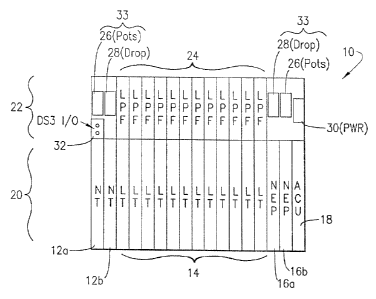
Fig. 1 shows a new shelf arrangement 10 for use in a
subscriber access multiplexer system according to the
invention. The embodiment shown is for use in an ATM
subscriber access multiplexer (ASAM) system, but it
should be understood that the invention is not limited to
ATM embodiments. The shelf 10 is populated by at least
one or a redundant pair of network termination (NT} cards
12a, 12b, up to twelve xDSL, in this case ADSL
(Asynchronous Digital Subscriber Line), line termination
(LT} cards 14, an equal number of Low Pass Filter (LPF)
cards 24, an optional Network Element Processor (NEP) 1.6a
(or an optional redundant pair 1.6a, ~.6b), and an Alarm
Collection Unit (ACU) 28. An LT card is described in
more detail below in connection with Fig. 10, while a
2 o network termination card is described in more detail
below in connection with Fig. 14A-14E~ A lowpass filter
card is disclosed in more detail below in connection with
Figs. 7A, 7B and 7C. An alarm collection unit (ACU) Z8
is shown in block diagram form in Fig. 15, and a physical
2 5 embodiment is shown in Fig. 16.
These cards can be mounted.as shown in Fig. 1 in a
bottom section 20 of the shelf 10 and can be, e.g., six
rack spaces in height where one rack space equals 1.75
inches (4.45 cm}. An upper portion 22 of the shelf can
3c3 be, e.g., three rack spaces in height for containing up
to, e.g., twelve lowpass filter (LPF} cards 24, with each
LPF card dedicated to an associated ADSL--LT directly
below it. Also in the upper portion 22 of the shelf 10
may be located connections 26 for POTS (plain old
3 5 telephone service) interfaces and connections 28 for drop
9
CA 02444231 2003-10-24
tip/ring leads, connections 3~ for power, and a small
board 32 for DS3NT equipment protection as explained
below. The POTS can, but need not, be in analog baseband
form. It could take other forms, such_as ISDN. Note
that the lowpass filters 24 are grouped in the center of
the upper portion 22 of the shelf, with the connections
26 for POTS and connections 28 for drop tip/ring leads
for location at ends 33 of the upper portion 22 of the
shelf. Since the lowpass filters plug into the backplane
upon insertion in slots of the shelf and do not connect
to cables, they are positioned in the center of the upper
portion 22. The connections 26, 28,.30 and 32, on the
other hand, require cabling access and are positioned,
according to the present invention, at the ends 33 to
facilitate such connections near the periphery of the
shelf 19, rather than requiring cables passing over
central portions of the shelf. Similarly, the LT cards
14 are positioned in the center of the lower section 20
of the shelf 10, since they do not require cabling and
are connected to other modules by the backplane, to which
they are connected via a connector upon insertion. Thus,
the NTs 12A, 12B, the NEPs 16A, 16B and the ACU 18 are
positioned at ends 35 of the lower section 20 to provide
easy cable access. It is also noted that the shelf is
designed entirely for front access. The shelf 10 can be
dimensioned to fit both U.S. and European equipment
racks, e.g., being X98 mm wide and 285 mm deep.
The ADSL-LTs and the LPFs are dimensioned as four
lines per card. As such, a basic shelf supports forty-
eight ADSL lines in a physical configuration shown in
Fig. 1.
Fig. 1A shows a front view of an actual shelf with
redundant NT cards, 12 LT cards, l2 corresponding LPF
cards, and an ACU card all inserted therein. Fig. 1B
3 5 shows a plurality of shelves mounted in a central off ice
1~
CA 02444231 2003-10-24
rack, such as shown in Fig. ~E, in a standard
configuration for serving 192 ADSL lines. Up to four
adjacent racks can share the same feeder by using
extension units installed in place of DTs, as explained
below in connection with Fig. 6. In tYhat case, a single~
optionally-protected NT card can support up to 576 ADSL
lines. Fig. 1C shows the she~.f of Fig. 1A without any
cards installed and shows the connectors installed in the
backplane, into which mating connectors on the cards are
insertable by sliding the cards into i~he slots shown. In
this way, front-access-only is achieved. A side view of
the shelf is shown in Fig. 1D.
It should be realized that without modification the
LTs could be located in the upper portion and the LI~Fs in
the lower pOrt~.On. Similarly, the var~.Otzs power and
COnneCtlOn S2CtlOns Can be located Other $:han aS ShOWn
eXlCtly 7.n Fl.g. ~.. Thus, the ATIJI SubSCrl.ber aCCP_SS
multiplexes (ASAM) shelf described above, although
unique, can have additional as well as other physical and
packaging arrangements to fit particular applications.
In addition to the above-described front-access-only
shelf compatible with both LT. S. and international racks,
the above-described shelf facilitates high density, i.e.,
small volume per l~.ne design. Also included is a
practical high-speed (155-622 Mb/s) backplane data bus.
It contains a simple, flexible shelf ID (:identification)
mechanism. Connectorization and wiring is designed for
future BITS capability. It satisfies both T1.S. and
European electromagnetic compatibility (F.~iC)
343 requirements. It includes card arrangement for NT and LT
cabling for T, coaxial, or fiber.
As suggested above, it can be utilized as a full-
sized LT shelf for maximum density and minimum cost, as
shown in Fig. 1B for a C~, or as described more fully
3.1
CA 02444231 2003-10-24
below in connection with Fig. ~ as a mini~-ized ( RAM
shelf for small remote sites.
The POTS lowpass filters (LPF) 24 of Fig. 1 can be
passive (filters that are contained as shown in separate
units for ensuring POTS immunity to xDSL failures,
maintenance and churn a.s well as for lower
digital/analog crosstalk. In other words, an LT card or
any other aspect of the ADSL channel c:an be maintained
without disturbing the POTS. Consequently, overall
performance is increased.
A functional block diagram of an LT/LPF pair fror<
the group Z4, 24 of Fig. 1 is shown serving a single
copper pair 36 in Fig.. 2. Although only a single twisted
copper pair 36 is shown, it should be realized that the
5.5 preferred embodiment includes four twisted copper pairs
per LT/LPF card pair. In other words, the LT/LPF blocks
shown within the ADSL shelf section 34 will be replicated
four times for each such LT/LPF pair shown in Fig. 1 {See
the LT card of Fig. 10).
2o As seen in Fig. 2, an ADSL data stream formatted as
ATM cells are transported over the copper pair 36
formerly used for telephony only (POTS service) in an
overlay fashion,, through the use of highpass (filters 38,
39 and lowpass filters 40, 42 at both the ADSL shelf to
25 the left of a dash line 44 and at the subscriber premises
on the right side of the line 44. The line 44 signifies
the place where copper distribution to the subscriber
begins. Normally, the ADSL shelf section 34 will be part
of a shelf 20 such as shown in Fig. 1A within a rack in a
3Q central ~ffice, as shown in Fig. 1B, within which off ice
also resides a CO switch 46 and a broadband switch such
as a packet switch, e.g., an ATM switch 4S. The
broadband switch could be located elsewhere, such as
further upstream. The c0 switch 46 is for connectiorn to
35 a switched telephone network, such as the public switched
12
CA 02444231 2003-10-24
telephone network (PSTIJ) for pro~idinc~ POTS service on a_
line 50 to the twisted copper pair 36 and into customer
premises via copper wires 52 at the customer end, as
shown in Fig. 2 on the right--hand side of a dashed line
54, signifying a customer premises boundary, for
connection to a telephone 56 for normal voice
communication. However, the ADSL shelf 34 could just as
easily be located in a remote cabinet in association with
a DLC (Digital Loop Carrier) shelf, as described further
below, with both ATM traffic and POTS being carried to
it, e.g., by a SONET (synchronous Optical NETwork)
transport product.
The ATM switch 48 is for connection to an ATM
network which provides connection to various services,
including Internet service Providers (ISPs) and other
high bandwidth service providers. The ATM switch 48
provides ATM formatted data on a line 58 to a network
termination (NT) card 60 which is, in turn, connected to
a plurality of ADSL line termination (LT) cards such as
the card 62 which includes the highpass filter 38 for
providing the ADSL signal on a line 64 to a junction node
66 for combination with the normal telephony signals
provided by the lowpass f alter 40. The node 66 thus
forms a.means for frequency division multiplexing, i.e.,
joining the POTS service on the line 50 at a low
frequency with the high bandwidth services provided on
the line 58 and converted to ADSL by the LT 62 at a
higher frequency for passing through the filter 38 and on
to the line 64 for combination with t:he telephony service
at the node 66 of the twisted copper pair 36. Fig. 12
(not to scale) shows an example of bandwidth allocation
for POTS service at baseband, e..g., d-4 k~iz, with DMT
technology used for the ADSL signal between 40 k~iz and
1.2 ~iHz. In this case, the spectrum allocated for use
downstream is much larger than that allocated for
13
CA 02444231 2003-10-24
°~.pstream, ana_ her~Ge the designatiam as °'as~rmmetr~_ca:L''
digital subscriber line (ADSL).
Referring back to Fig. 2, at the customer end 54, a
node 68 allows the signal on t3.le line 36 to be split off
on a line 70 before passing a telephony signal through a
lowpass filter 42 in a Network Interface Device (NID)
(not shown). The NID can be an enclosure (box) for
mounting on the wall of a house, and both the node 68 and
LPF 42 can be inside the NID. The line 70 is Connected
to an ADSL modem 72 which highpass filters the signal on
the line 70 and demodulates and decodes the ADSL signal
for providing a high bandwidth signal on a line 74 to
customer premises equipment such as, but not limited to,
a personal computer (PC) 76. The NID enclosure can be,
for example, a.s shown in copending and co-owned patent
application filed on even date herewith entitled '°
Apparatus for Mounting a Low Pass Filter in a Telephone
Network Interface Box" having U.S. Serial No. (Atty.
Docket No. 907-158) now U.S. patent No. 6,044,151.
It should be mentioned that the F~OT'S signals in the
baseband part of the signal spectrum of the signal on the
line 36 of Fig. 2 can include conventional analog modem
and even mechanized loop testing (MLT) signals, neither
of which will be degraded by or affect the ADSL service.
The functional block diagram shovtn in Fig. 2
illustrates both the data and telephony paths to the
customer. The shelf (basic shelf) architecture is
further illustrated in Fig. 3. The basic shelf 1Q
includes an °'IQ bus" including control leads 78, which is
more fully described in copending U.B, provisional patent
application Serial No. (Atty. Docket No. 9a2-583)
entitled 'eMethod for Prioritized Data Transmission and
Data Tran~mi_ssion Arrangement'°, filed on even date
herewith (see E.P. 0881853, as mentioned previously). As
was known in the prior ar_t, whenever a number of any
14
CA 02444231 2003-10-24
kind of terminal units need to access a common medium or
bus, some access grant criterion is needed, e.g., upon a
grant signal, each terminal unit enters an arbitration
phase based on the respective priority values assigned to
the terminal unit. The problem with this is a problem of
fairness, in that the terminal having a low priority
might never get access. In brief, and as illustrated in
Fig. 3A, the IQ bus invention makes the priority
adaptable after each grant cycle, so that if a unit does
not get access, its priority can be increased. In
addition, the priority value can be linked to an access
mode requested by the terminal unit, e.g~,. a Guaranteed
Cell Rate GCR (CBR, VBR, ABR in case of an ATM-based
bus), Non-Guaranteed Cell Rate NGCR (VBR, ABR, EBR in
case of an ATM-based bus) by allocating value ranges 'to
each access mode, increase of the priority then being
limited by the boundaries of the respective ranges. For
instance, five different levels of QoS classes are shown
at the left-hand side of Fig. 3A, with the lower three
classes having both guaranteed cell rate and non-
guaranteed cell rate subclasses indicated.o Naturally,
the constant bit rate (CBR) and variable bit rate-real
time (VBRrt) classes do not have non-guaranteed cell rate
(NGCR), since they must be guaranteed.. The non-
guaranteed cell rates are shown grouped at the bottom of
the priority mapping to the right, which shows Qos
subclasses with guaranteed subclasses at the top
(shaded). Nevertheless, according to. the present
invention, overbooking of non-guaranteed bandwidth is
3o allowed by providing not only prioritisation, as shown,
but also an aging mechanism, as shown: on the far right of
Fig. 3A. When a terminal subscribing to a non-guaranteed
class of service does not get access within a
predetermined period, its priority is increased according
to a selected algorithm to a value within a range
CA 02444231 2003-10-24
eorrespondi.ng to an access znode having a higher aCCess
probability. One particular and non-limiting way of
defining priority values is suggested in fig. 3A, with
215-1 priority values defined and evenly allocated (for
instance) among the QoS subclasses. As an example, for a
hardened-UBR QoS class, the guaranteed cell rate (GCR) is
normally defined as a number of cells per second. A
period having a time defined by the inverse thereof can
thus be defined as shown in Fig'. 3A, indicating how the
priority of the cell from the lowest subclass (Non-
Guaranteed Hardened UBR) can be increased after it is n.ot
granted access to the bus after a waiting time T = 1/GCR
seconds. ~Cn the example shown, the priority is increased
in a single step t~ that of the Guaranteed lHardened UBR
subclass,thus statistically implementing a minimum cell
rate for the lowest subclass. These teachings
advantageously provide a flexible method allowing access
based on a type of access mode and on agreed access
parameters. The IQ bus is thus distinguished by a unique
grant mechanism and fairness algorithm. It provides
multiple Q~S classes with multiple cell priorities per
class. It features a cell aging priority mechanism, as
well as a QoS priority mechanism to ensure cells comply
with the class of service parameters defined in Bellcore
Specification GR-1110. It is provided wi-th fault
tolerance and recovery mechanisms, allowing any fault on
the multiplex bus to be quickly identified and isolated.
It has a redundant extension capability as well, as
described below in connection with Fig. 6. The IQ 'bus
builds upon an earlier "I* bus°' (without QoS) described
in copending U.S. provisional patent application Serial
loo. (Atty. Docket Tao. 9t~2-~S1) entitlecz "Priority-Based
Access Control Method and Arrangement'°, filed an even
30 data herewith, (which gave rise to L~.S. patent No.
6, i05, 084 ) . --
16
CA 02444231 2003-10-24
As shown in both. Figsa 2 and 3, the NTs l2aP 12b can
be provided in either a redundant or non-redundant
configuration. In this architecture, the normal NE
processing is performed by the NT, and the NT can be
provided as either a SONET User Network. Interface (UNI)
interface, a DS-3 UNI interface or later, a DS1 inverse
multiplex UNI interface. If SONET NT;~ are provided as
redundant pairs, Automatic Protection Switching (APS) is
provided using the normal 1+1 switchover mechanism
detailed in Bellcore document GR-253. On SONET NTs, the
physical interface (fiber) is located on the faceplate of
the NT itself {see Figs l~C and 1~D), with no need of
additional interface circuitry. If, however, NTs are
provided as DS-3 ports, equipanent protection (without
cable protection) is provided using the DS-3 I/O board 32
shown in Fig. 1 installed above the NTs ire the shelf,
allowing the single DS-3 facility (coax cable Tx/Rx pair)
to be split and accessed by either NT (inter-NT
communication arbitrates which one is active).
From the foregoing it will be appreciated that the
heart of the ADSL shelf architecture is the above-
mentioned I~ bus and control leads '~8. The IQ bus
effectively acts as a multiplexer at the eaame effective
speed as the NT physical interface. Since ADSL-LTs
provide several classes.of service (as deffined in
Bellcore document GR-111Q and the ATM Forum Standards), a
grant mechanism allows higher priority upstream cells
greater access to this ATM MLTX bus, in order to meet the
QoS parameters required of the respective services
provided. As mentioned, two methods of cell priority can
be chosen to guarantee QoS requirements and relative
fairness--a weighting priority mechanism (based om
service guarantees) and an aging mechanism (based on time
a cell has been waiting for a grant). This mechanism is
unique and the subject of the above-mentioned provisional
17
CA 02444231 2003-10-24
application Serial No. (Atty Docket 902-583), (see E.P.
0881 853 as mentioned previously).
The ACU 18 in Fig. 3 is shown in lalock diagram form
in Fig. 15, and it performs the following functions: (1)
collects eternal customer designated alarm contacts on
lines 80 and forwaras these events to 'the NT 12a via
lines 78; (2) collects failure indications in the rack
and forwards this information to the NT 12a; (3) receives
processed alarm data from the NT and displays the alarm
condition (critical, major, minor) on the ACU's faceplate
as well as providing contact closures for visual and
audible (and telemetry alarms) to a rack fuse panel and
to a CO alarm interface via a line 82. The ACU also
contains: (4) an alarm cutoff (ACO) function to silence
audible indications until a new alarm is detected (as
well as a remote ACO function via line 82); (5j a craft
interface port 84 for controlling O.AZ~I and P functions of
the ADSL NE (using a link to the processor in the NT);
(6) an ethernet port for OS cannection via the NEP; anal
(7) a lamp test function. One ACU card is provided per
rack when .a system spans multiple racks. An ACU is
provided per NT (or redundant NT pair;' when multiple
systems reside in a given rack. I~ult:iple systems res~_de
in a given rack when a very wide bandwidth is to be
served by, e.g., a single shelf. In ;such a case, a
single shelf may use up the entire ba~.dwidt2~. of an OC-~3
or DS-3 cable.
As shown in Figs. 3 and 10, each Ai7SL~ LT 14a, 143,
..., 141 communicates with up to four remote modems (ADSL
NT or ANT) at corresponding customer premises via DNiT
(Discrete lMulti-Tone) per T1.413 (see Fig. 12) , using .ATM
cells as the data transport format, according to the
present invention. The subscriber can have a lowpass
filter (LPF) 42 mounted, for example, on the outside wall
of his home in an NTD (Network Interface Device) boy t~
1~
CA 02444231 2003-10-24
separate the low frequency service (telephony) from the
higher frequency services (ADSL). As mentioned, a way to
mount such an LPF within an existing design NID is shown in
copending application U.S. Serial No. (Atty. Docket 907-
158) filed on ever. date herewith, now U.S. patent hlo.
6,044,151. The two services, once split, use different
twisted pairs in the house wiring, with the ADSL pair
terminating in either an ANT,or directly in a PC via an NIC
(Network Tnterface Card). ANTS, for example, can come in
two types: one with an ATMF 25.6 Mb/s interface, the other
with an ethernet interface (in this case the ANT packages
the ethernet data as ATM cells using AAL5 (ATM Adaptation
Layer 5) protocol)e Both options can be provided on the
same ANT, as shown in Fig. 13B.
The basic shelf 1~ also contains, as shown in Figs.
1 and 3, an optional network element processor (NEP)
redundant pair 16a, 16b, whieh communicates over the I
bus 78 mechanism and communicates with its redundant
partner over separate leads 86 to determine which one is
active. The NEP can terminate signaling channels for PVC
(switched virtual connection] services or PVC (permanent
virtual connection) services and can terminate the ACU
ethernet port.
Presently, the two NEP cards 16a, 16b of Figs~ 1. and
3 are not being implemented, although there are two slots
reserved for it. It is planned to be available later fox'
terminating and processing SVG (Switched Virtual Circuit)
signaling channels, and for providing an ethernet
termination for the ACU ethernet portF There are no
other functions presently planned for the 1~EP cards.
As shown ire Fic~. 4, the basic, shelf ~.p may a:l_so be
used as a °°hub°° she:Lf X08 ~a~_th one or more
ADSL°~zT slots
populated by US~~°~LTs or other ca~°d~ bauch as QC-°~8,
I5S~~1
inverse m~z~ hTs F etc . Each hS~._~ ~h~ connects the hub to a
19
CA 02444231 2003-10-24
concatenated "remote" fiDSL shelf ~6, ~8, aS Srlown 131 Fag.
In Such cases, for the hub, tile "LPF" riodules abOVe
the DS-3-LTs are replaced with DS-3-LT interface modules
(one type for nonredundant operation and another type for
redundant DS-3 "equipment protection" operation). A
third type of DS-3 LT interface module can. be provided
for redundant IQ bus operation, with the DS-3-LTs being
on separate shelves for reliability purposes (due to
there being only one IQ bus per shelf). The present
architecture uniquely provides for each of these
redundancy options.
As shown in Fig. 4A, the LT-LPF backplane wiring is
shown With LT transceivers. In this case, the LPF and LT
cards can be configured for redundancy of the LT cards to
be inserted in the LT slots in either' a same shelf or in
separate shelves. For example, in Fi.g. 4B, a non-
redundant option LT is shown with a rrs-3 interface
inserted in LPF slot 1, wherein input and output DS-3
coax cables from a C~ switch are connected to a DS-3
interface card for insertyon in LPF slot 1, which is
connected through the backplane to a DS-3-LT card for
insertion in LT slot 1, such as the nS3-LT card 92 of
Fig. 4. The lowpass filter function is carried out at
the remote shelf 96 of Fig. ~ where a DLC is available.
2 ~ The conf iguration shown in Fig. 4B for LT' slot 1 and LPF
slot 1 could also be used in connection with Fig. 4E,. as
explained below.
Fig. 4C shows an application with redundant DS-~3-LT
cards for insertion, a~g., in LT slot ~. and LT slot ~ of
3 ~ a given shelf . Ire that case, a. different kind of DS-3
I/O card is used, double wide as shown, with a center
tapped transformer on the card which is connected both to
the transmit cTxA/TxB) and to the receive (~tXA/RXB)
backplane wiring associated. with both LPF slot 2 and LPF
3 5 slot 2. The NT controls which LT slot is to be active~
CA 02444231 2003-10-24
Fig. 4D is similar to Fig. 4A but additionally shows
arbitration interfaces between redundant DS-3LTs.
As suggested above, since there s.s only one
nonredundant IQ bus per shelf, the equipment protection
implied by Fig. 4C with A and B redundant DS-3-LT cards
in slots 1 and 2 will be ineffective if the IQ bus itself
has a failure. If it is desired to avoid this sort of
failure, a different kind of redundancy in the DS-3 cards
can be provided, as shown in Fig. 4E. In that case, half
l0 of the transmit and receive signals are used in the
shelf, and the other half can be routed to a different
shelf, instead of slot 2 in the same shelf. The top two
cables shown in Fig. 4E would thus be routed to.another
shelf and be connected into, e.g., the DS-3 out and DS-3
in transformers shown in Fig. 4B in another shelf. The
DS-3 out and DS-3 in cables of Fig. 4E would go to the CO
switch or other network element.
As will be observed 1n Fig. 4, an ADSL shelf 90 may
have both ADSL-LTs 14a and aggregate type LTs such as the
DS-3LTs 92, 94 shown. Service classes in both cases are
provided for subscribers by separate buffers per service
class (CBR, VBR, UBR, etc.), each conaending for upstream
access to the IQ bus via the control leads and the grant
mechanism based in part on the priors.ty a:~signed to each
upstream cell. In the case of aggregate LTs, such as
shown in the hub 9~ of Fig. ~, the s~:rvic' class buffers
have a cell priority equal to the sum of the aggregate
cell priorities in each buffer (or even some percentagey,
in order that the remote subscribers are assigned a fair
share of the hub's operating bandwidth. In times of
bursty upstream traffic, congestion and DS-3-LT buffer
overflow is managed by limiting the DS-3 link bandwidth
and allawing temporary buffer fill in the remote ADSL-LTs
(until such time that the traffic peak subsides). It is
noted that POTS interfaces are not shown in Fig. 4 but
21
CA 02444231 2003-10-24
would narmally be provided, e.g., by O~LCs adjacent or
incorporated in the Remotes 9~, 98.
Fig. 5 shows the hub 90 of Fig. ~: located in a
central office 100 which may also inc3_ude a CO switch 102
and an ATM switch 104. The CQ switch is connected to a
public switched telephone network {PS~'~) 106 and the ATM
switch to an ATM network 208 which is,, in turn, connected
to other services 110 which may include various Internet
service providers 112, ..., 114. As illustrated in Fig.
4, the hub shelf 90 may be populated by both ADSL LT
cards such as the card 14a and various other cards
including DS-3 LT cards 92, 94. Four copper pairs
emerging from the ADSL LT card 14a of Fig. 4 are
illustrated as a plurality of copper ;pairs 11~ in both
25 Figs. 4 and 5. These leads provide a:n ADSL link directly
between the hub and the various customer premises
illustrated, including a customer premises 118 shown in
detail. If the shelf 90 were used exclusively with ADSL
LTs 14, such as shown in Fig. 1, all of the subscriber
lines would be like the lines 116 without using the shelf
90 as a hub and without the remotes of Fig. 5. In other
words, there would be twelve groups of 4 POTS plus ADSL
lines 116 serving 48 different customer premises. The
implementation of Fig. 5 provides for many more customer
premises served by a single shelf, but with the
accompanying increased competition for upstream
bandwidth. This can be tolerated in cases where the
majority of subscribers are using lower quality of
service.
A lowpass filter 120 is mounted in a network
interface device arrangement (not shown) for terminating
the subscriber line at the customer's premises. It
filters out all but the low frequency telephony signal
from the copper pair and provides it on a line 122 to a
traditional telephone 124 for voice communications: It
22
CA 02444231 2003-10-24
also filters high frequency dial pulse or ring trip
transients so that they do not interfere in the upstream
direction with the high-speed data traffic. A second
copper pair connected before the lowpass filter, as
shown, is provided to an ADSL modem 126 which, after
highpass filtering, demodulates and decodes the ADSL
signal and provides output bits on a line 128 to a user
terminal 130 such as a personal computer, Internet
computer, etc., e.g., for Internet access or for access
to other high bandwidth services 110. It should be
realized that the ADSL modem also operates in the reverse
(upstream) direction, albeit in a much narrower
bandwidth, to encode and modulate bites owto the ADSL line
from the subscriber to the ATM network as per ANSI T1.4 13
(see Fig. 12) .
The remote shelves 96, 98 of Fig. 4 are also shown
in Fig. 5 connected to various customer premises, which
are similar to premises 118.
Fig. 6 shows in detail the above-mentioned feature
of the present architecture whereby a plurality of ADSL
Shelves 10a, 10b, 10c, 10d such as sl:aown iri Fig. 1 Cari be
daisy-chained together in a rack by means of ari extender
card (EXT) in each subsequent shelf. The extender card
function is to effectively extend the IQ bus from shelf
2 5 to shelf (daisy-chained, e.g., to a maximum of twelve
shelves altogether), allowing up to, e.g., 576 ADSL
subscribers accessed to the system. Tn other words, the
extender card allows an NT card in a first shelf to act
as an NT card for another shelf or a. plurality of other
shelves. I.e., in this case, three racks with altogether
twelve daisy-chained shelves. The extender cards can be
mounted as shown in Fig. 6 in the NT slots of subsequent
shelves arid may be redundant. Iri that case, any failure
of an NT or extender card bank switches all LTs frore~ the
"A" NT/extender String to the "E" string. The active
23
CA 02444231 2003-10-24
string then assumes control of each shelf's IQ bus. The
IQ bus itself (within each shelf) is not redundant, but
meets reliability requirements, as the NT has the ability
to remove each LT from the IQ bus (disable) to isolate a
fault and remove it from service.
As suggested above, the POTS lowpass filters can be
provided for different options including "integrated" in
a CO shelf for maximum packaging denvsity, minimum cabling
and installation complexity and minimum cost as described
1 O above or "separate" (remote, non-integrated) for
regulatory flexibility and access to existing (crowded)
DLC cabinets.
Fig. 7A shows a lowpass filter card, such as one of
the LPF cards 24 shown in Fig. 1 in schematic~block
diagram form. Four different lowpass filters/splitters
are shown on the card. To the left of each card is a
voice port for connection to the narrowband (NB) network
via the CO switch 46 via the line 50. On the righthand
side of each lowpass filter/splitter is a port which is
2 O connected both to the twisted copper pair 36 to the
subscriber and to the highpass filter 3S of the LT 62
(see Fig. 2). A side view of the physical dimensions of
such a four-channel LPF card is shown in Fig. 7~, while a
front view is shown in Fig. 7C.
2 5 Fig .. 7D shows a splitter shelf for use in
applications where the iowpass filters need to be remote
from the ADSL shelf. Such a shelf can be used, for
example, when (a) separate service providers are
responsible for the telephony and ADSL services, or (b)
3 O in DLC (digital loop carrier) configurations where remote
cabinets of DLC equipment cannot accommodate ADSL
equipment (due to lack of physical space), but since the
subscriber transmission pairs terminate an the DLC
cabinet (and enough room is available for a small lowpass
24
CA 02444231 2003-10-24
ffilter "splittera'), this shelf only is installed in the
DLC cabinet.
In this case, the basic xDSL shelg isn used, as
previously shown, but with the LPF boards not populated.
A separate "splitter' shelf, as Shawn in Fig. 7, is then
provided and has a configuration the same as, or vary
much like, the top portion of the basic xDSL shelf 10 of
Fig. 1. The main difference in remote sputter
configurations is the cabling and the use of "stackable'
connectors. The splitter shelf is shown in Fig. 7, and a
typical configuration using splitter she7_ves is shown in
Fig. 8. In an initial imple~raentation, LPFs (and the
splitter shelf) need no power, as a17_ circuitry is
passive.
Fig. 8A shows a remote cabinet that can be used when
adding ADSL service to existing metallic-fed DLCs. 'I~his
configuration supports up to 96 linen in .a type 3002
cabinet.
Tt should be noted that the "separateness" of the
lowpass filters 24 as shown in Fig. 1 from the LTs, as
well as the separateness of the LPFs of Figs. 7, 8 and 8A
is not only advantageous for the reason mentioned above,
i.e., for facilitating separate service providers for.
telephony and ADSL services, but also for the very
important reason, according to the present invention, for
physically separating the lifeline telephony service from
the ADSL service. Such separateness provides an
increased level of integrity for the lifeline POTS
service, since such physical separateness itself ensures
3 O that any maintenance actions which may need to be
performed on the ADSL part of the system can be done in a
physically separate manner, and therefore in such a way
as to not affect the POTS service (and vice versa).
Another equipment she7_f is the RAM Remote ADSL Mux)
3 5 shelf as shown in Fig. 9. This shelf is deployed very
CA 02444231 2003-10-24
i
much like the remote ADSL shelves 96, 98 shown in Fig. 4,
and in fact may have the same shelf architecture as that
shown in Fig. 3. The difference is that the RAM shelf is
more suited for CPE or DLC applications where, e.g., no
more than twenty-four lines are required, and a smaller
shelf (6RS versus 9RS) is desired. As such, a RAM shelf
may be designed and physically configured, for example,
as shown in Fig. 9. This shows the flexibility of the
xDSL shelf of the present architecture.
Fig. 10 shows a functional block diagram of one of
the ADSL LT cards 14a of Figs. 1, 3 and 4. The
implementation of the various functional blocks is
realized in this implementation by the application of an
ADSL chip set of assignee for DMT technology. This chip
, set consists of three chips (integrated circuits)
identified as RCHAP for ATM functions, a DACHAJSACHA chip
for Reed Solomon coding and decoding, and a front-end DSP
chip called ADSLB. The remaining blocks are preferably
carried out by other means outside th.e chip set. The
three chip chip set RCHAP, SACRA and ADSL13 are also shown
in Fig. 11 in a simplified block diagram that shows the
chip set in both an LT 14a in an ADSL shelf 34 and in an
ADSL modem 72 at a customers premises in reverse
ordering of chips.
In regard to the ATM functions carried out by the
RCHAPB chip, such takes care of the encapsulation of ATM
cells in 54-byte slots and the access to two separate IQ
buses, i.e., upstream and downstream. There is also a
dummy cell added to the 53 standard P.TM cells in order to
allow a change-over from one LT to another on the
upstream IQ interface (between cells). On the downstream
IQ interface, this byte is not filled in, and on the
upstream IQ interface, the bus is in high impedance state
during this byte.
26
CA 02444231 2003-10-24
The main entity which is conveyed through an AT~i
network is a cell which is divided into two parts, each
with a fixed sizes the header (5 bytes), and the
information field (48 bytes). Depending on the value of
the header of the ATM cell, a number of ATM-related
functions may be performed, such as illserti.On and
extraction of maintenance cells, cell rate decoupling,
Header Error Control (HEC) generation,/check, payload
scrambling, cell loopback, etc.
The data that are sent on the ADSL line are forward
error- corrected (FEC) by Reed Solomon (RS) coding to
improve the bit error rate. To allow for an even better
protection against burst errors an interleaving
possibility is incorporated, with the disadvantage of an
increased transfer delay for interleaved data. Also, a
scrambler is included to randomize the data before the RS
encoder. After the RS decoder, the data is then
descrambled.
Also carried out by the SACRA chip set, besides Reed
Solomon (de)coding is mapping and demapping. In the ADSL
system, a DMT approach may be followed in which, for
example, up to two hundred fifty-six carrier frequencies
can be used (see Fig. 12). Each of these frequencies
will carry a number of bits according to a mapping table.
The function of the mapper is to assign the bits to the
different frequencies. The mapper can also send some
special DMT symbols for link initialization and
maintenance. The demapper will demodulate and monitor
the received symbols. After demodulation, it delivers
the data to the on~chip RS decoder. Some special
functions are included in the demapper for initialization
and maintenance of the ADSL link. An example of an ADSL
mapper is shown in Fig~ 1 of copending and co-owned
application Serial No. ~8/677,468, filed July 10, 1996
and described at page 7, line 5, through page 9, line 23.
27
CA 02444231 2003-10-24
A simila~° description is given in. copending pxovisional
application Serial No. (Atty. Docket No. 902-575) filed
on even date. herewith, entitled "Method and Windowing
Unit to Reduce Leakage, Fouriex Transformer and DMT Modem
Wherein the Unit is Used", at page 5, line 10, through
page 7, line 26 thereof (which gave rise to U.S. patent No.
6, 240, 129) .
The output of the mapper is a complex representation
of all the carrier frequencies. An Inverse Fast Fourier
Transformer is used to transform th~.s representation to a
time signal. In cooperation with the IFFT, a carrier
selective scaling can be installed. In the upstream
direction, an FFT is used to transform the received time
signal to a frequency representation.
The main function of the front-end digital signal
processing is to separate the received signal as much as
possible from the transmitted signal, and to correct for
the line and analog front-end characteristics.
The ADSLB chip function includes analog-to-digital
(A/D) and digital-to-analog (D/A) conversion: The
function of the subscriber line analog front end is the
termination of the analog line interface and the
transformation of the digital data into an analog
passband signal that can b~ transmitted on a physical
subscriber line 36 and vice versa. For the D/A and Aj?D
conversion, a sigma-delta (ED) approach is used.
As shown in Fig. 11, the subscriber line analog
front-end function includes a line driver used to amplify
the ADSLB output to the levels appropriate to be
transmitted over the subscriber line. A hybrid is
included as a passive network that performs the
termination of the subscriber line with its nominal
impedance and handles the conversion between four-wire
and two-wire in the LT at the upstream end. Tt performs
the separation in the upstream direction between the
upstream and downstream signals, and the combining in the
28
CA 02444231 2003-10-24
downstrean direction. The re~rerse is performed at the
downstream end of the line.
Referring back to Fig. 1U, it is noted that the LT
14a includes four separate line termination paths for
four separate subscribers. Although not shown in Fig. 10
or 11, it should be realized that the twisted pair
connects not only to the HP-filter and hybrid shown in
Figs. l0 and 11, but also to a lowpass filter 40, such as
shown in Fig-. 2. Fig, 10A shows a front view of an LT
card, while Fig. 10B shows a side view.
Since POTS signals and ADSL signals are transported.
frequency-multiplexed on a subscriber line, as shown in
Fig. 12, a POTS lowpass filter 26 is required, which
performs the following functions: (1) combining the PO'JC'S
and ADSL transmit signals toward the subscriber premises;
(2) separating the POTS and ADSL signals from the
subscriber premises; (3) protecting the POTS from audible
interference, generated by signals from tree ADSL modern
and the ADSL shelf; and (4) protecting the ADSL receiver
from all POTSrelated signals, particularly dial pulses,
ringing and ring trip transients.
These functions are performed while meeting all the
requirements for POTS performance, such as return loss,
insertion hoss and group delay, such as those in ANSI
Standard T1.413. The combination and separation of POTS
and ADSL signals is achieved by lowpass arid highpass
filtering, as shown in Fig. 2. only the highpass filter
and the hybrid are part of the LT. A.s mentioned abave,
the lowpass part preferably resides on a different
3~ printed board assembly (LPF).
Also shown in Fig. 1.0 is an on-board controller
(OBC),.which may be embodied as a microprocessor included
to handle a variety of tasks, such as initialization of
ASTCs, monitoring and processing of maintenance messages,
and detection of a malfunctioning LT. On--board memory
29
CA 02444231 2003-10-24
may include flash-PROM and DRAM used for executable code
and data. Inventory information may also be stored on an
EEPROM so as to provide the necessary data for an
adequate identification of a replaceable item. Such may
include product identification, manuf<~.cturing information
and inventory information. Also shown in Fig. 10 are
power supply functions by way of on-board mounted DC/DC
converters. A test access port (not shown) may also be
provided.
As will be understood by anyone of skill in the art,
from American Rational Standard for Telecommunications
"Network and Customer Installation Interfaces--Asymmetric
Digital Subscriber Line (ADSL) Metallic Interface"Y ANSI
T1.413-1995, the~nature of the signal on the twisted pair
36 shown in Fig. 11 and in Fig. 2 may be a standardized
asymmetric digital subscriber line signal that allows the
provision of plain old telephone service (POTS) and a
variety of digital channels. In the direction from the
network to the customer premises, the digital channels
2o may consist of full duplex low-speed channels and simplex
high-speed channels; in the upstream direction, only low-
speed channels are provided. The transmission system is
designed to operate on two-wire twisted metallic cable
pairs with mixed gauges. The standard is based on the
use of cables without loading coils, but bridged.taps are
acceptable, with the exception of unusual situations. As
shown in Fig. 12, for example, the power spectrum is
shown as including a 4 l'~Fiz band reserved for POTS
service, with the portion of the spectrum between 40 KHz
and l.1 MHz occupied by a large plurality of carriers,
with tone spacing of 4.3125 I~Hz. A small portion of the
spectrum is used far upstream data, as shown, with the
remainder used for downstream data. Each of the 4 KHz
tones is QAM-modulated and individually selected and
optimized as a function of individual subscriber line
CA 02444231 2003-10-24
characteristics. Some tones are allocated with a large
number of bits, while others a lesser number or none at
all, due to line conditions.
As shown in Fig. 11, the functions already described
in connection with an ADSL LT 14a are replicated in the
ADSL modem 72. In addition, a selected interface to the
subscriber PC 76 may include, e.g., an ATM-25 and/or
Ethernet interface, as shown in Fig. 11.
Fig. 13A shows a simplified block diagram
illustration of an ADSL Network Termination (ANT) unit.
Tt includes a modem part which perfo~~us the ATU-R
transmitter reference model functions, for example, as
shown in Section 4.3 of ANST T1.413-1.95. An ATM
function is added, according to the present invention,
for ATM translation and signal processing. In the
downstream direction, the ANT unit terminates the ADSL
signal, demodulates, and the interconnect function
converts the ATM cells into a digital bitstream to the
subscriber's digital terminal equipment (DTE). In the
2~ embodiment shown, the interfacing block to the customer
equipment includes both ATE! and/or ethernet interfaces,
as shown. Fig. 13B shows an ADSL Network Termination
Unit with the line, ATM and ethernet connections shown.
The line connector is RJ34, while the ATMF-25 and lOF3ase-
T connectors are RJ45, fig. 13C shows five LED
indicators that are visible an the top of the box of Fig.
13B for giving the indications indicated in the table of
Fig. 13D .
A more detailed functional block diagram of an ADSL
3 O modem 72 (such as already shown in Fig. 11) is shown in
Fig. 13. The lowpass filter 42 of Fig. 2 is shown as
part of an external "splitter" in Fig. 23, which also
includes the node 68 of Fig. 2.,
An external AC/DC inverter (6V DC/xV AC) and an on~
3 5 board DC/DC power supply are shown in Fig. 13 and are
31
CA 02444231 2003-10-24
used to feed the power to the board. The external pocaer
supply (AC/DC) converts the high voltage from the wall
outlet to a voltage that can be handled by the ADSL modem
:2, such as -3-6 volts DC. Further conversions are shown
from the DC/DC power supply.
An analog front-end may include the highpass filter
39 already shown in Fig. 2, as well as a hybrid and line
driver such as shown in Fig. 11. The hybrid is far 2-
wire to/from 4-wire conversion.
l0 An ADSLB block is shown for terminating the analog
line interface and for transformation of digital data
from a DACHA/SACHA block into an analog passband signal
that can be transmitted on a physical subscriber line and
vice versa. The ADSLB performs analog-to-digital (A/D)
and digital-to-analog (D/A) conversion.
Again, the SACHA is the DMT signal
modulator/demodulator. This software-configured ASIC
processes the ATM cells (scrambled) from the RCHAP block
and delivers the DMT modulated signal to the ADSLB and
2o vice versa. Note that there is no difference between the
DACHA and the SACHA, except a lower cost for the SACRA.
A DACHA can be used as well, and is especially necessary
to support a standardized 4.3125 biz tone spacing mode.
The RCHAP provides the interconnection between the
SACHA/DACHA and the rest of the system. It contains l6
ATM cell buffers in both upstream and. downstream
directions, and performs virtual path/virtual channel
(VP/VC) translation, extraction and insertion of ATM
cells, and handles on-board tasks.
A RAPID block provides interfacing between RCHAP,
ATM-izer and IDT-PIiY blocks. It also contains DMA
controller and logic for ethernet functions.
fihe IDT-PHY block translates ATM cells between the
on-board parallel data bus (with standard byte-wide
32
CA 02444231 2003-10-24
cells) and the seryal data over the ATM Forum physical
connector (with scrambled 485B coded data).
The ATM-izer is the upstream controller, responsible
for upstream quality of service, cell shaping and
policing. It is responsible for translating downstream
AAL5 packets into ethernet-frames and vice versa.
Handling upstream ATM Forum data is also performed by the
ATM-izer.
An 182596 controller performs CSMA/CI5 medium-access
to control, moves ethernet frames between SRAM packet memory
and a.serial ethernet transceiver. It is monitored by
the OBC. An 182503 performs a serial transceiver
function to 802.3 ~.OBase-T, direct interface. to I82596.
For code processing, an I960 microprocessor is
included to handle a variety of tasks, sucyh as
initialization of ASICs, memories, etc., monitoring and
processing of the maintenance messages, on-line/off-line
test support. Memory is included in the OBC as well,
such as 2 Mb DRAM for program executables and a 1.5 Mb F-
PROM for boot code, power-Ori test, a 512 Kb for ethernet
packet memory, etc. A small EEPROM (4 Kbit) is used for
a remote inventor circuit.
Fig. 14A shows a simplified block diagram of an
embodiment of an NT card, according to the present
invention. It provides a high-speed optical or
electrical access to a Synchronous Optical Network
(SONET) transport system. It converi~s Asynchronous
Transfer Mode (ATM) cells to SONET packets (i.e., frames)
and vice versa. Thus, the NT card adapts ATM cells
3 O carried on the IQ bus to the SONET transmission system
and vice versa. It also includes necessary functions as
listed in the table of Fig. 14B for operating and
maintaining the ATM subscriber access multiplexer of the
present invention.
33
CA 02444231 2003-10-24
It is noted that the table of Fig. 14B is split into
two columns representing downstream functions and
upstream functions. The downstream functions, for
example, have been grouped and numbered 1--4; and
similarly labeled in Fig. 14A in the top section of the
respective four blocks. similarly, for the upstream
functions, these have been grouped in the right-hand side
of the table and have been numbered 5-8, with the same
numbers shown in the lower half of the blocks of Fig.
14A. It should be realized that these functions can be
moved between blocks, and this is just an example.
In regard to the physical medium block, this can be
an optical interface for interfacing an optical transport
system with a receive and transmit optical fiber carrying
1 ~ signals, e.g., with a nominal bit rate of 155.52 Mbps.
The interface is symmetric, i.e~, it has the same bit
rate in both directions and could operate, e.g., at a
wavelength of ~..3 ~Sm. This signal c<~n be a SONET
(.Synchronous Optical Networks signal at the OC-3 level
2 O for conversion to STM-liSTS-3c in the electrical domain.
This is a serial signal which the physical medium
interface block converts to parallel form. at a slower
rate for processing on the NT card, with the parallel
downstream output locked on to the received clock.
2 5 The transmission convergence sublayer processing is
done in the second block, wherein the ATM cells are
delineated within a hierarchical transmi.slion frame
structure used to transport the ATM cells. These cells
are divided into two parts, each with a fixed s~.ze, the
3 0 head with five octets, as shown in Fig. 14F, and the
payload with 48 octets, as shown in fig. 14H. In the ATI~
block of Fig. 14A, ATM layer processing is carried out.
In the upstream direction, all fields in the ATM cells
received on the IQup interface are transported
35 transparently, except for the Header Error Control (HEC)
34
CA 02444231 2003-10-24
ffield (see ITU-T Recommendation Im361, 'B-ISDN ATN Layer
Specification). The HEC may be checked or not, as an
option. The routing of received ATM cells depends upon
the VPI (Virtual Path Identifier) and i?CI (Virtual
Channel Identifiers bits in the cell header. The full
VPI octet and the eight least significant bits of the VCI
can be checked for VPI/VCI combinations corresponding
with a data channel to be extracted. This method
provides for a maximum of 216 channels which can be marked
for extraction. All valid cells received from the IQ
interface are transmitted either upstream in a virtual
container or synchronous payload envelope (VC-4/SPE, or
to an on-board controller.
For downstream ATM layer processing in the ATM block
of Fig. 14A; each VC-4/SPE carries the equivalent of
44.151 cells (53 octets) which are octet-aligned and
floating within the VC-4/SPE. The ATM cell delineation
uses the correlation between the Header Error Control
(HEC) in the cell header and the cell header itself. The
cell delineation mechanism, as recommended by ITU-T
Recommendation I.432, 'B-ISDN User-Network Interface-
Physical. Layer Specification, is used. ~7hen the ATM
cell boundary identification in octet Ii4 is used, the
cell delineation will start searching' at the octet
indicated by H4. If not, the search will start at the
first octet of the payload period. The ATM cell
information fields are descrambled according to the self-
synchronizing scrambling/descrambling~ scheme recommended
by ITU-T.
Valid non-idle cells, each with its confirmed ~IEC
octet and descrambled information field, are sent t~ the
IQ down interface, which is the last block shown in Fig.
14A. In that block, idle cell periods are added to adapt
a received bit rate of up to 149.76 Mbit/s to 152.64
Mbit/s.
~5
CA 02444231 2003-10-24
The routing of received ATI~ cells depends upon the
VPI, VCI and PTI (payload type identifier) bits in the
cell header. In total, 16 bits or four nibbles of
VPI/VCI combinations can be checked, according to the
modes shown in Fig. 14G. In each mentioned mode,
different nibbles of VPT/VCI are selected. The selected
VPI/VCI nibble combination corresponds with a specific
data channel to be extracted. Cells can be extracted by
looking only at the VPI/VCI combination or by looking at
the VPI/VCI combination and at the PTI bits. In the
second case, each PTI (23 in total) can be marked for
extraction. This marking will then be used for all
VPI/VCI combinations for which extraction is indicated,
with the inclusion of the PTI-check. A11 valid cells
received in the virtual cantainer or synchronous payload
envelope, independent of their VPI/VC'I combination, are
transmitted downstream on the IQ down interface (cells
marked for extraction are also sent to the ATM interface
bus) .
ATM cell insertion and extraction is provided at the
NT both in the direction of the network and in the
direction of the I~ bus, in order to provide for the
transmission and reception of Operat~_on A.nd Maintenance
and signaling cells. Cell insertion and extraction i.s
under control of an On-Board Controller (OBC).
In the upstream direction, the OBC has the
possibility of inserting ATM cells in the outgoing VC-
4/SPE. The OBC has to provide a valid cell header
without HEC, followed by a least six bytes and, at most,
3o the complete cell payload (a total o~ 52 octetsj. The
HEC is calculated before the cell is put into the VC--
4/SPE. Interfacing between the OBC and upstream cell
stream is performed by using a FIFO buffer on which a
back pressure signal indicates if the OBC is allowed to
insert a cell or has to wait until the previously
36
CA 02444231 2003-10-24
inserted cell is transmitted. Cells received on the =Q
up interface have a higher priority irhan cells coming
from the OBC. Synchronization is performed by a
synchronization signal which indicates tc the cell
insertion device where the boundary between two inserted
cells in the FIFO buffer is. Downstream, the OBC has the
possibility of inserting ATM cells irs the IQ down cell
stream. The OBC has to provide a valid cell header
without HEC, followed by at least six bytes and at most
1 O the complete cell payload (a total of 52 octets). The
HEC is generated when transmitted onto the IQ interface.
Interfacing between the OBC and the downstream cell
stream is performed by the same cell FIFO buffer as for
the upstream cell insertion. Also for downstream cell
1 5 insertion, a back pressure mechanism is implemented.
Cells received in the VC-~JSPE have a higher priority
than cells from the OBC. Synchronization is performed by
a synchronization signal, which indicates to the cell
insertion device where the boundary between two inserted
2 O cells in the FIFO buffer is.
For cell extraction in the upstream direction, such
is performed using the cell filtering mechanism described
above. Only the first four octets .of the cell header and
the comp lete payload are extracted from the IQ up
2 5 interface. For interfacing between the extraction
circuitry and the OBC, a FIFO buffer is used. The OBC
should synchronize to the extracted cell.stream by
reading blocks of 52 octets until th.e buffer is empty.
Downstream cell extraction is performed using the
3 O cell filtering mechanism mentioned above. Only the first
four octets of the cell header and the complete payload
are extracted from the VC-4/SPE. Before a possible
extractionP the HEC in these cells is alL~eady checked for
errors. For interfacing between the: extraction circuitry
3 5 and the OBC, ~ FIFO buffer is used: The OBC should
37
CA 02444231 2003-10-24
synchs oniz ed to tree extracted yell stream by r ~eadi_.ng
blocks of 52 octets until the buffet is eanpty. The cell
which is extracted towards the oBC can optionally be sent
to the IQ down interface also.
As suggested above, the IQ down a~~d I~ up buses
transport ATM cells with a five~octet header and a 48-
octet information field. In front of each cell is one
dummy octet, illustrated in Fig. 14H. The ATM cells are
encapsulated in 54 octet slots and provided access to the
IQ bus. The adaptation of 155.52 Mbit/s to 152.64 Mbit/s
(53/54*155.52 Mbitjs) is performed by the deletion of
idle cells. This can be done due to the fact that the
maximum bit rate of valid ATM cells contained in the VC-
4sJSPEs is limited to 149.76 Mbit/s {26-27k155.52
Mbit/s).
The dummy octet is added to the ATM cells in order
to allow a changeover from one LT to another on the IQ up
interface (between cel7~s) . On the IQ down interface,
this octet is not ffilled in, on the IQ up interface, the
bus is in high impedance state during this octet.
The NT card is managed by an ADSh wor~~station {AWS)
which may be located in an operating system (OS) as shown
in Fig. 5. Such an OS may communicate through an ATM
network and an ATM switch in a central office. with the ~1T
card in the shelf. See copending and co-owned U.S.
patent application S/N (Arty. Docket No. 907-160) (now U.S.
patent No_ 5,991,814} entitled "ASAM Network Management
System with Open Loop Flow Control", filed on even state
herewith fox further details. Fig. 14C shows a front triew
anti Fig. 14D a side view of an NT card., such as may be used
in a slot of a shelf of Fig. 1.
Fig. 14E shows a more detailed functional block
diagram of an NT card 12a of Fig, 1. An
optical/ehectrical transceiver provides a SODIET/SDI~
38
CA 02444231 2003-10-24
compliant interface for 155.52 Mbps STM1 or STS3-c
signals in one integrated package. Clock recovery is
clone in the S/UNI+. In order to dc this clock recovery,
it requires a reference clock. The recovered clock
(155.52 Mliz) is divided by eight in the S/UNI+ and serves
as one of the inputs for serving as a reference clock to
a PLL circuit located in a UIAC block to which a VCXO
output clock must track (if loop timing is enabled). The
resulting clock out of the VCXO serves as input clock for
to transmit data towards the optical transceiver, where this
clock is used to synthesize the transmit clock, and which
also serves as a system clock. The reference clock input
and the VCXO output clock are further divided by a faotor
N in the UIAC (N = 2048 for Bellcore and N.= 128 for
ITU). After a phase comparison between the two resulting
divided clocks, the resulting voltage: is fed to a lo~rrpass
filter, after which the signal drives the VCXO. Loop
timing can be established by locking the transmit clock
(system clock) on the receive clock.
At the ATM side of the S/UNI+ there are two internal
four-cell synchronous FIFO's present that are controlled
by the UIAC. This interface acts as an SCI/PHY (Utopia-
like),interface. Back pressure (upstream) is inherently
present due to the FIFO~s integrated in the S/UNI. For
the upstream direction, this means that if there is a
_.___ full load of 155.52 Mbps on the IQ~bus (152.64 Mbps at
the Utopia interface) and a maximum transmit capacity of
149.76 Mbps ATM cells, the four-cell FIFO will be full
after 1.5 ms.
~O The UIAC component is an LCA device which is
programmed during 'power-on-reset" from a serial PROM.
It uses. three syncrgronous 512 x 9 bit. FIFOs for cell
insertion and extraction and one 128K x 8 bit SRAM for
routing. The UIAC module has a SCI/PHY (Utopia-like)
interface to the S/UNI+ component. ATM cell insertion in
39
CA 02444231 2003-10-24
both the direction of the network (SDH/SONET) and in the
direction of the LTs is handled by a 1 SIF (signaling
insertion. FIFO) buffer. An oBC bus is connected directly
to the eight data inputs of the FIFO. The direction of
cell insertion is specified by the OBC by writing into an
additional UIAC register. The ninth bit of the FIFO is
used for cell synchronization and insertion direction
specification. A RAM lookup table is used far cell
filtering on VPI/VCI combinations. The RAM has 128K
to entries ~f eight bits.
Downstream cell extraction is performed by a
downstream signaling extraction FIFO (DSEF), The eight-
bit output data of this buffer is c~nnected to a
peripheral bus. A~1 cells which are extracted are copied
by default to the downstream traffic stream. This can be
disabled, however, by a traffic control register in the
UIAC.
Upstream cell extraction is performed via the USEF
{upstream signal extraction FIFO). The eight-bit output
data of this buffer is connected to the peripheral bus.
A cell received on the upstream IQ interface is sent
either t~ the OBC or to the upstream SDB/SONET interface.
All cells which are extracted are copied by default to
the upstream traffic stream. This can be disabled,
however, by the traffic control register in the UIAC.
In the downstream direction, ATM cells are
transferred to an rCOM interface. In the upstream
direction, ATM cells are received from the ICOM.
The UIAC may be equipped by a boundary scan
interface conforming to IEEE 1149.1 (STAG) Specification.
A block diagram of an ADSL Alarm Control Unit (ACU)
is shown in Fig. 15A, while the funct?ons thereof are
listed tri.e table of Fig. 158. Fig. 1~ shows a front view
and Fig. 17 a side view of the ACU.
~0
CA 02444231 2003-10-24
In addition to the foregoing disclosure,
reference may be made to the following disclosures of
relevance:
U.S. Pat. No. 5,636,253, issued June 3, 1997,
entitled "Method for Detecting Erasures in Received Digital
Data" ;
U.S. Pat. No. 5,633,817, issued May 27, 1997,
entitled "Fast Fourier Transform Dedicated Processor";
U.S. Patent Application Serial No. 08/561.,445,
filed November 21, 1995, entitled "Signal Processor
Module", disclosing ADSL selective DPLL (now U.S. Pat. No.
5, 657, 355) ;
U.S. Fatent Application Serial No, 08/560,938,
filed November 20, 1995, entitled "Signal Processor"
disclosing a DMT-based transceiver (now U.S. Pat. No.
5,768,318) ;
U.S. Patent Application Ser_i.al No. 08/593,885,
filed January 30, 1996, entitled "Frequency Division
Multiple Access (FDMA) Dedicated Transmission System,
Transmitter and Receiver Used in Such a System", disclosing
a DMT modem for multiple access (now U.S. Pat. No.
5,809,030);
U.S. Patent Application Serial No. 08/677,468,
filed July 10, 1996, entitled "Method for Allocating Data
Elements in Multicarrier Applications and Equipment to
Perform This Method", disclosing ADSh bit allocation (now
U.S. Pat. No. 5,812,599);
U.S. Patent Application Serial No. 08/675,323,
filed July 10, 1996; entitled "Method of Allocation Data
Elements to a Set of Carriers, Mapping Unit and Modulator
41
CA 02444231 2003-10-24
to Perform this Method" , disclosing an ADSL BIGI Algorithm
(now U.S. Pat. No. 5,790,550);
U.S. Patent Application Serial No. 08/700,756,
filed August 15, 1996, entitled "Method for Interleaving
Data Frames, Forward Error Correcting Device and Modulator
Including Such a Device", disclosing interleaving in ADSL
(now U.S. Pat. No. 5,907,560);
U.S. Patent Application Serial No. 08/718,641,
filed September 1'7, 1996, entitled "Sensing Circuit",
disclosing an activity detector for ADSL, where the CO is
quietly awaiting for remote activity (ncw U.S. Pat. No.
5, 963, 885) ;
U.S. Patent Application Serial No. 08/729,429,
filed October 11, 1996, entitled "Method for Transmission
Line Impulse Response Equalization and a Device to Perform
this Method", disclosing an ISI reduction algorithm in an
analog (front-end) transceiver (now U.S. Pat. No:
5,870,432);
U.S. Patent Application Serial No. 08/783,859,
filed January 16, 1997, entitled "Method and Modem for
Adaptive Allocation of the Pilot Carrier in a Multi-Carrier
System", disclosing DMT pilot tone reallacation (now U.S.
Pat. No. 5,867,528);
U.S. Provisional Application Serial No. (Atty.
Docket No. 902-575) filed on even date herewith, entitled
"Method and Windowing Unit to Reduce Leakage, Fourier
Transforme r and DMT Modem, Wherein the Unit is Used",
disclosing single frequency or banded noise immunity (which
gave rise to U.S. Pat. No. 6,240,129);
LT. S. Provisional Application Serial No. (Atty.
Docltet No. 902-576) entitled "Transmitter with Phase Rotor,
42
CA 02444231 2003-10-24
Modulator/Demodulator, Communications System and Method
Performed Thereby" , disclosing a rotor for DMT (which gave
rise to U.S. Pat. No, 6,088,386);
U.S. Provisional Application Serial No. (Atty.
Docket No. 902-577) entitled "Method to Transparently
Transport an Incoming Clock Signal over a Network Segment
and Related Transmitter and Receiver Unit"', disclosing an
ATM time reference transport aver ADSL (which gave rise to
U.S. Pat. Tto. 6,327F273);
U.S. Provisional application Serial No. (Atty
Docket No. 902-578) entitled "A Method to-Synchronize Data
and a Transmitter and Receiver Realizing Said Method"
disclosing reversal of clacks for ATM over ADSL (which gave
rise to U.S. Pat. No. 5,903,612);
U.S. Provisional Application Serial No. (Atty.
Docket No. 902-579) entitled "Initialization ProLOCOl for
Adaptive Data Rates and Related Transceiver", disclosing
ADSL rate renegotiation (which gave rise to U.S. Pat. No.
6,215,793);
U.S. Provisional Application Serial No. (Atty.
Docket No. 902-580) entitled "Method to Allocate Data Bits,
Multicarrier and Transmitter and Receiver Using the Method,
and, Related Allocation Message", disclosing RFI reduction
in DNT systems (which gave rise to U.S. Pat. No.
6,351,473);
U.S. Provisional Application Serial No. (Atty.
Docket No. 902-581) entitled "Priority-Based Access Control
Method and Arrangement", disclosing an earlier I* bus for
connecting an NT to LTs (which gave rise to U. S . Pat . No .
6,105,084);
4 .3
CA 02444231 2003-10-24
U.S. Provisional Application Serial No. (Atty.
Docket No. 902-582) entitled "Current Control Interface
Arrangement", disclosing a power-up circuit (which gave
rise to U.S. Pat No. 5,951,660);
U.S. Provisional Application Serial No. (Atty.
Docket No. 902-583) entitled "Method for Prioritized Data
Transmission and Data Transmission Arrangement", disclosing
a preferred IQ bus for connecting an NT to LTs, as
described in Fig. 3 above (which. gave rise to EP
application No. 0 881 853 published on December 2, 1998);
U.S. Provisional Application Serial No. (Atty.
Docket No. 902-585? entitled "Multicarrier Telecom System
with Power Adaptation Means" (which gave rise to U.S, Pat.
No. 6,246,'725) .
Although the invention has been shown and
described with respect to a best mode embodiment thereof,
it should be understood by those skilled in the art-that
the foregoing and various other changes, omissions and
additions in the form and detail thereof rnay be made
therein without departing from the sps.rit and scope of the
invention.
44