Note: Descriptions are shown in the official language in which they were submitted.
CA 02444296 2003-10-09
WO 02/084709 PCT/US02/11461
HIGH PRESSURE PROCESSING CHAMBER
FOR SEMICONDUCTOR SUBSTRATE
INCLUDING FLOW ENHANCING FEATURES
RELATED APPLICATIONS
This application claims priority from U.S. Provisional Patent Application No.
60/283,132, filed on April 10, 2001, which is incorporated by reference.
FIELD OF THE INVENTION
This invention relates to the field of high pressure processing. More
particularly, this
invention relates to the field of high pressure processing of a semiconductor
substrate.
I0 BACKGROUND OF THE INVENTION
Processing of semiconductor substrates presents unique problems not associated
with
processing of other workpieces. Typically, the semiconductor processing begins
with a
silicon wafer. The semiconductor processing starts with doping of the silicon
wafer to
produce transistors. Next, the semiconductor processing continues with
deposition of metal
and dielectric layers interspersed with etching of lines and vies to produce
transistor contacts
and interconnect structures. Ultimately in the semiconductor processing, the
transistors, the
transistor contacts, and the interconnects form integrated circuits.
A critical processing requirement for the processing of the semiconductor
substrate is
cleanliness. Much of semiconductor processing takes place in vacuum, which is
an
inherently clean environment. Other semiconductor processing takes place in a
wet process
at atmospheric pressure, which because of a rinsing nature of the wet process
is an inherently
clean process. For example, removal of photoresist and photoresist residue
subsequent to
etching of the lines and the vies uses plasma aching, a vacuum process,
followed by stripping
in a stripper bath, a wet process.
Other critical processing requirements for the processing of the semiconductor
substrates include throughput and reliability. Production processing of the
semiconductor
substrates takes place in a semiconductor fabrication facility. The
semiconductor fabrication
facility requires a large capital outlay for processing equipment, for the
facility itself, and for
a staff to run it. In order to recoup these expenses and generate a sufficient
income from the
facility, the processing equipment requires a throughput of a sufficient
number of the wafers
in a period of time. The processing equipment must also promote a reliable
process in order
to ensure continued revenue from the facility.
Until recently, the plasma aching and the stripper bath were found sufficient
for the
removal of the photoresist and the photoresist residue in the semiconductor
processing.
However, recent advancements for the integrated circuits include etch feature
critical
dimensions below dimensions with sufficient structure to withstand the
stripper bath and low
dielectric constant materials which cannot withstand an oxygen enviromnent of
the plasma
aching.
CA 02444296 2003-10-09
WO 02/084709 PCT/US02/11461
Recently, interest has developed in replacing the plasma ashing and the
stripper bath
for the removal of the photoresist and the photoresist residue with a
supercritical process.
However, high pressure processing chambers of existing supercritical
processing systems are
not appropriate to meet the unique needs of the semiconductor processing
requirements. In
particular, high pressure chamber of existing supercritical processing systems
do not provide
a flow speed adequate to remove particulate matter from a surface of the
semiconductor
wafer.
What is needed is a high pressure processing chamber for semiconductor
processing
which provides adequate flow speed over a surface of a semiconductor
substrate.
SUMMARY OF THE INVENTION
The present invention is a high pressure chamber for processing of a
semiconductor
substrate comprising a high pressure processing cavity, a plurality of
injection nozzles, and
first and second outlet ports. The high pressure processing cavity holds the
semiconductor
substrate during high pressure processing. The plurality of injection nozzles
are oriented into
the high pressure processing cavity at a vortex angle and are operable to
produce a vortex
over a surface of the semiconductor substrate. The first and second outlet
ports are located
proximate to a center of the plurality of injection nozzles and are operable
in a first time
segment to provide an operating outlet out of the first outlet port and
operable in a second
time segment to provide the operating outlet out of the second outlet port.
In an alternative embodiment of the present invention, an upper surface of the
high
pressure processing cavity comprises a height variation. The height variation
produces more
uniform molecular speeds for a process fluid flowing over the semiconductor
substrate.
BRIEF DESCRIPTION OF THE DRAWINGS
FIG. 1 illustrates a pressure chamber frame of the present invention.
FIG. 2 illustrates a first alternative pressure chamber of the present
invention.
FIG. 3 illustrates a cross-section of the first alternative pressure chamber
of the
present invention.
FIGS. 4A and 4B illustrate a spacer/injection ring of the present invention.
FIG. 5 illustrates a wafer cavity and a two port outlet of the present
invention.
FIG. 6 illustrates a supercritical processing module and a second alternative
pressure
chamber of the present invention.
FIGS. 7 illustrates the wafer cavity of the present invention.
FIGS. 8A-8C illustrate first through third alternative wafer cavities of the
present
invention.
FIG. 9 illustrates the preferred pressure chamber of the present invention.
FIGS. 10A and lOB illustrate an upper cavity plate/injection ring of the
present
invention.
CA 02444296 2003-10-09
WO 02/084709 PCT/US02/11461
DETAILED DESCRIPTION OF THE INVENTION
The preferred pressure chamber of the present invention is preferably used for
supercritical processing of a semiconductor wafer. Preferably, the preferred
pressure
chamber forms part of a supercritical processing module. Preferably, the
supercritical
processing module is used to remove materials such as photoresist, photoresist
residue, and
etch residue from the semiconductor wafer. Alternatively, the supercritical
processing
module is used for other supercritical processing of the semiconductor wafer,
such as
photoresist development.
A pressure chamber frame of the present invention is illustrated in FIG. 1.
The
pressure chamber frame 10 includes a pressure chamber housing portion 12, a
hydraulic
actuation portion 14, a wafer slit 16, windows 18, posts 19, a top opening 20,
and top bolt
holes 22. The wafer slit 16 is preferably sized for a 300 mm wafer.
Alternatively, the wafer
slit 16 is sized for a larger or a smaller wafer. Further alternatively, the
wafer slit 16 is sized
for a semiconductor substrate other than a wafer, such as a puck.
The hydraulic actuation portion 14 of the pressure chamber frame 10 includes
the
windows 18, which provide access for assembly and disassembly of the preferred
pressure
chamber. Preferably, there are four of the windows 18, which are located on
sides of the
pressure chamber frame 10. Preferably, each of the windows 18 are framed on
their sides by
two of the posts 19, on their top by the pressure chamber housing portion 12,
and on their
bottom by a base 23. The bolt holes 22 of the pressure chamber housing portion
12 are for
bolting a top lid to the pressure chamber frame 10.
Before describing the preferred pressure chamber of the present invention,
first and
second alternative pressure chambers of the present invention are described in
order to more
simply introduce aspects of the present invention.
The first alternative pressure chamber of the present invention is illustrated
in FIG. 2.
The first alternative pressure chamber 30 includes the pressure chamber frame
10, the top lid
32, a wafer platen 34, a cylinder 36, and a sealing plate 38. The top lid 32
is coupled to the
pressure chamber frame 10, preferably by bolts (not shown). The wafer platen
34 is coupled
to the cylinder 36. The cylinder 36 is coupled to a piston (not shown). The
sealing plate 38
seals the piston from atmosphere.
It will be readily apparent to one skilled in the art that fasteners couple
the wafer
platen 34 to the cylinder 36, couple the cylinder 36' to the piston, and
couple the sealing plate
38 to the pressure chamber frame 10. Further, it will be readily apparent to
one skilled in the
art that the bolts which preferably couple the top lid 32 to the pressure
chamber frame 10 can
be replaced by other fasteners, such as by screws or by threading the pressure
chamber frame
10 and the top lid~32.
A cross-sectional view of the first alternative pressure chamber 30 in a
closed
configuration is illustrated in FIG. 3. The first alternative pressure chamber
30 includes the
pressure chamber frame 10, the top lid 32, the wafer platen 34, the cylinder
36, the sealing
plate 38, the piston 40, and a spacer/injection ring 42. Preferably, the
pressure chamber
CA 02444296 2003-10-09
WO 02/084709 PCT/US02/11461
frame 10, the top lid 32, the wafer platen 34, the cylinder 36, the sealing
plate 38, the piston
40, and the spacer/injection ring 42 comprise stainless steel. The
spacer/injection ring 42, the
top lid 32, and the wafer platen 34 form a wafer cavity 44. The wafer cavity
44 is preferably
sealed with first, second, and third o-rings (not shown) located in first,
second, and third o-
'S ring grooves, 48, 50, and 52. The pressure chamber frame 10 and the sealing
plate 38
enclose a piston body 54 leaving a piston neck 56 extending through the
sealing plate 38.
The piston neck 56 couples to the cylinder 36, which in turn couples to the
wafer platen 34.
The pressure chamber frame 10 and the piston body 56 form a hydraulic cavity
58
below the piston body 56. The pressure chamber frame 10, the sealing plate 38,
the piston
body 54, and the piston neck 56 just above the piston body 54 form a pneumatic
cavity 60
between the piston body 54 and the sealing plate 38.
Tt will be readily apparent to one skilled in the art that a piston seal
between the piston
body 54 and the pressure chamber frame 10 isolates the hydraulic cavity 58
from the
pneumatic cavity 60. Further, it will be readily apparent to one skilled in
the art that a neck
seal, between the piston neck 56 and the sealing plate 38, and a plate seal,
between the
sealing plate 38 and the pressure chamber frame 10, isolate the pneumatic
cavity 60 from
atmosphere. Moreover, it will be readily apparent to one skilled in the art
that in operation
hydraulic and pneumatic fluid systems, both of which are well known in the
art, are coupled
to the hydraulic cavity 58 and the pneumatic cavity 60, respectively.
In the supercritical processing, the semiconductor wafer 46 occupies the wafer
cavity
44 where a supercritical fluid is preferably used in conjunction with a
solvent to remove the
photoresist from the semiconductor wafer 46. Preferably, the wafer platen 34
comprises a
vacuum chuck, which holds the semiconductor wafer 46 during the semiconductor
processing. After the supercritical processing and venting of the wafer cavity
44 to
atmospheric pressure, hydraulic fluid within the hydraulic cavity 58 is
depressurized while
the pneumatic cavity 60 is slightly pressurized with a gas, which moves the
piston 40 down.
This lowers the wafer platen 34 so that the semiconductor wafer 46 is adjacent
to the slit 16.
The wafer 46 is then removed through the slit 16. Preferably, the
semiconductor wafer is
removed by a robot (not shown). Alternatively, the semiconductor wafer 46 is
removed by a
technician.
A second semiconductor wafer is then loaded through the slit 16 and onto the
wafer
platen 34. Next, the pneumatic cavity 60 is vented to atmospheric pressure
while the
hydraulic cavity 58 is pressurized with the hydraulic fluid, which drives the
wafer platen 34
into the spacer/injection ring 42, which reforms the wafer cavity 44. The
wafer cavity 44 is
then pressurized, and the supercritical fluid and the solvent remove the
photoresist from the
second wafer.
It will be readily apparent to one skilled in the art that during the
supercritical
processing the hydraulic fluid within the hydraulic cavity 58 must be
maintained at an
hydraulic pressure which causes an upward force that is greater than a
downward force on the
wafer platen 34 caused by the supercritical fluid.
CA 02444296 2003-10-09
WO 02/084709 PCT/US02/11461
The spacer/inj ection ring 42 of the present invention is further illustrated
FIG. 4A.
The spacer/injection ring comprises a ring body 62 having a plenum 64 and
injection nozzles
66. Preferably, the spacer/injection ring 42 has an inside diameter of
slightly greater than 12
inches, which is sized for the 300 mm wafer. Alternatively, the
spacer/injection ring 42 has a
larger or smaller inside diameter. Preferably, the spacer/injection ring has
forty-five of the
injection nozzles 66. Alternatively, the spacer/injection ring has more or
less of the injection
nozzles 66. Preferably, each of the injection nozzles 66 is oriented at
45° to a radius of the
inside diameter of the spacer/injection ring 42. Alternatively, the injection
nozzles are at a
larger or smaller angle. Preferably, the spacer/injection ring 42 has a
thickness of .200
inches. Alternatively, the spacer/injection ring 42 has a larger or smaller
thickness.
A cross-section of the spacer/injection ring 42 is illustrated in FIG. 4B,
showing the
ring body 62, the plenurn 64, and one of the injection nozzles 66. Preferably,
the plenum 64
has a rectangular cross-section having a width of .160 inches and a height of
.110 inches.
Preferably, each of the injection nozzles 66 has a diameter of .028 inches.
The plenum 64
and the injection nozzles 66 of the spacer/injection ring 42 form a passage
for the
supercritical fluid entering the wafer cavity 44 (FIG. 3). In the
supercritical processing, the
supercritical fluid first enters the plenum 64, which acts as a reservoir for
the supercritical
fluid. The supercritical fluid is then injected into the wafer cavity 44 by
the injection nozzles
66, which creates a vortex within the wafer cavity 44 (FIG. 3).
The wafer cavity 44 and a two port outlet of the present invention are
illustrated in
FIG. 5. The wafer cavity 44 formed by the top lid 32, the wafer platen 34, and
the
spacer/injection ring 42 is preferably exhausted through the two port outlet
70. The two port
outlet 70 includes a shuttle piece 72, which is alternated between a first
position 74 and a
second position 76. By alternating the shuttle piece 72 between the first and
second
positions, a center of the vortex formed by the spacer/injection ring 42 will
alternate between
a first exhaust port 78 and a second exhaust port 80. Preferably, the first
and second exhaust
ports, 78 and 80, have a diameter of .40 inch and have centers separated by a
distance of 1.55
inches. Alternatively, the diameter and the distance are larger or smaller
depending upon the
specific implementation of the present invention:
In operation, incoming supercritical fluid 82 enters the plenum 64 of the
spacer/injection ring 42, creates the vortex within the wafer cavity 44, and
alternately creates
first and second vortex centers proximate to the first and second exhaust
ports, 78 and 80, as
the shuttle piece moves from the first position 74 to the second position 76.
Outgoing
supercritical fluid 84 then exits the two port outlet 70. In this way, the
supercritical
processing of an entire surface of the semiconductor wafer 46 is assured.
It will be readily apparent to one skilled in the art that the injection
nozzles 66 of the
spacer/injection ring 42 and the two port outlet 70 can be incorporated into a
general pressure
chamber having ingress and egress for a semiconductor substrate through a gate
valve.
Further, it will be readily apparent to one skilled in the art that the
shuttle piece 72 of the two
port outlet 70 can be replaced by a more general valve arrangement. Moreover,
it will be
CA 02444296 2003-10-09
WO 02/084709 PCT/US02/11461
readily apparent to one skilled in the art that additional outlet ports can be
added to the two
port outlet 70.
The supercritical processing module of the present invention, incorporating a
second
alternative pressure chamber of the present invention, is illustrated in FIG.
6. The
S supercritical processing module 200 includes the second alternative pressure
chamber 30B, a
pressure chamber heater 204, a carbon dioxide supply arrangement 206, a
circulation loop
208, a circulation pump 210, a chemical agent and rinse agent supply
arrangement 212, a
separating vessel 214, a liquidlsolid waste collection vessel 217, and a
liquefying/purifying
arrangement 219.
The second alternative pressure chamber 30B includes an alternative pressure
chamber housing 12A and an alternative wafer platen 34B. The alternative
pressure chamber
housing 12A and the alternative wafer platen 34B form a first alternative
wafer cavity 44A
for the semiconductor substrate 46. The alternative pressure chamber housing
12A includes
alternative injection nozzles 66A and an alternative two port outlet 70A.
Preferably, the
1 S alternative wafer platen 34B is held against the alternative pressure
chamber housing 12A
using a hydraulic force. Alternatively, the alternative wafer platen 34B is
held against the
alternative pressure chamber housing 12A using a mechanical clamping force.
Preferably,
the alternative wafer platen 34B moves to a load/unload position 21 S by
releasing the
hydraulic force. Alternatively, the alternative wafer platen 34B moves to the
load/unload
position 21 S upon release of the mechanical clamping force. Further
alternatively, the
alternative wafer platen 34B moves to the load/unload position 21S by
actuating a drive
screw coupled to the alternative wafer platen 34B or by using a pneumatic
force.
The carbon dioxide supply arrangement 206 includes a carbon dioxide supply
vessel
216, a carbon dioxide pump 218, and a carbon dioxide heater 220. The chemical
agent and
2S rinse agent supply arrangement 212 includes a chemical supply.vessel 222, a
rinse agent
supply vessel 224, and first and second high pressure injection pumps, 226 and
228.
The carbon dioxide supply vessel 216 is coupled to the second alternative
pressure
chamber 30B via the carbon dioxide pump 218 and carbon dioxide piping 230. The
carbon
dioxide piping 230 includes the carbon dioxide heater 220 located between the
carbon
dioxide pump 218 and the second alternative pressure chamber 30B. The pressure
chamber
heater 204 is coupled to the second alternative pressure chamber 30B. The
circulation pump
210 is located on the circulation loop 208. The circulation loop 208 couples
to the second
alternative pressure chamber 30B at a circulation inlet 232 and at a
circulation outlet 234.
The chemical supply vessel 222 is coupled to the circulation loop 208 via a
chemical supply
3S line 236. The rinse agent supply vessel 224 is coupled to the circulation
loop 208 via a rinse
agent supply line 238. The separating vessel 214 is coupled to the second
alternative
pressure chamber 30B via exhaust gas piping 240. The liquid/solid waste
collection vessel
217 is coupled to the separating vessel 214.
The separating vessel 214 is preferably coupled to the liquefying/purifying
arrangement 219 via return gas piping 241. The liquefying/purifying
arrangement 219 is
CA 02444296 2003-10-09
WO 02/084709 PCT/US02/11461
preferably coupled to the carbon dioxide supply vessel 216 via liquid carbon
dioxide piping
243. Alternatively, an off site location houses the liquefying/purifying
arrangement 219,
which receives exhaust gas in gas collection vessels and returns liquid carbon
dioxide in
liquid carbon dioxide vessels.
The pressure chamber heater 204 heats the second alternative pressure chamber
30B.
Preferably, the pressure chamber heater 204 is a heating blanket.
Alternatively, the pressure
chamber heater is some other type of heater.
Preferably, first and second filters, 221 and 223, are coupled to the
circulation loop
208. Preferably, the first filter 221 comprises a fine filter. More
preferably, the first filter
221 comprises the fine filter configured to filter 0.05 ~,m and larger
particles. Preferably, the
second filter 223 comprises a coarse filter. More preferably, the second
filter 223 comprises
the coarse filter configured to filter 2-3 ~,m and larger particles.
Preferably, a third filter 225
couples the carbon dioxide supply vessel 216 to the carbon dioxide pump 218.
Preferably,
the third filter 225 comprises the fine filter. More preferably, the third
filter 225 comprises
the fine filter configured to filter the 0.05 ~.m and larger particles.
It will be readily apparent to one skilled in the art that the supercritical
processing
module 200 includes valuing, control electronics, and utility hookups which
are typical of
supercritical fluid processing systems. Further, it will be readily apparent
to one skilled in
the art that the alternative injection nozzles 66A could be configured as part
of the alternative
wafer platen 34B rather than as part of the alternative chamber housing 12A.
In operation, the supercritical processing module is preferably used for
removing the
photoresist and photoresist residue from the semiconductor wafer 46. A
photoresist removal
process employing the supercritical processing module 200 comprises a loading
step, a
cleaning procedure, a rinsing procedure, and an unloading step.
In the loading step, the semiconductor wafer 46 is placed on the alternative
wafer
platen 34B and then the alternative wafer platen 34B is moved against the
alternative
chamber housing 12A sealing the alternative wafer platen 34B to the
alternative chamber
housing 12A and, thus, forming the first alternative wafer cavity 44A.
The cleaning procedure comprises first through fourth process steps. In the
first
process step, the first alternative wafer cavity 44A is pressurized by the
carbon dioxide pump
218 to desired supercritical conditions. In the second process step, the first
injection pump
226 pumps solvent form the chemical supply vessel 222 into the first
alternative wafer cavity
44A via the chemical supply line and the circulation loop 208. Upon reaching
desired
supercritical conditions, the carbon dioxide pump stops pressurizing the first
alternative
wafer cavity 44A. Upon reaching a desired concentration of the solvent, the
first injection
pump 226 stops injecting the solvent. In the third process step, the
circulation pump 210
circulates supercritical carbon dioxide and the solvent through the first
alternative wafer
cavity 44A and the circulation loop 208 until the photoresist and the
photoresist residue is
removed from the semiconductor wafer. In the fourth process step, the wafer
cavity 44A is
partially exhausted while maintaining pressure above a critical pressure, then
the first
CA 02444296 2003-10-09
WO 02/084709 PCT/US02/11461
alternative wafer cavity 44A is re-pressurized by the carbon dioxide pump 218
and partially
exhausted again while maintaining the pressure above the critical pressure.
The rinsing procedure comprises fourth through seventh process steps. In the
fourth
process step, the first alternative wafer cavity is pressurized by the carbon
dioxide pump 218.
In the fifth process step, the second injection pump 228 pumps a rinse agent
form the rinse
agent supply vessel 224 into the first alternative wafer cavity 44A via the
rinse agent supply
line 238 and the circulation loop 208. Upon reaching a desired concentration
of the rinse
agent, the second injection pump 228 stops injecting the rinse agent. In the
sixth process
step, the circulation pump 210 circulates the supercritical carbon dioxide and
the rinse agent
through the first alternative wafer cavity 44A and the circulation loop 208
for a pre-
determined time. In the seventh process step, the first alternative wafer
cavity 44A is de-
pressurized. Alternatively, it may be found that the fifth and sixth process
steps are not
needed.
In the unloading step, the alternative wafer platen 34B is moved to the
load/unload
position 215 where the semiconductor is removed from the alternative wafer
platen 34B.
Preferably, at least two of the supercritical processing modules of the
present
invention form part of a multiple workpiece processing system, which provides
simultaneous
processing capability for at least two of the semiconductor wafers. The
multiple workpiece
processing system is taught in U.S. Patent Application No. 09/704,642, filed
on Nov. 1, 2000,
which is incorporated in its entirety by reference. Alternatively, the
supercritical processing
module of the present invention along with a non-supercritical processing
module forms part
of a multiple process semiconductor processing system. The multiple process
semiconductor
processing system is taught in U.S. Patent Application No. 09/704,641, filed
Nov. 1, 2000,
which is incorporated in its entirety by reference. Further alternatively, the
supercritical
processing module of the present invention forms part of a stand-alone
supercritical
processing system employing a single supercritical processing module of the
present
invention.
The wafer cavity 44 of the first alternative pressure chamber 30 of the
present
invention is further illustrated in FIG. 7. (Note that in FIG. 7, a horizontal
scale has been
shortened by a factor of .75 and a vertical scale has been expanded by a
factor of four relative
to the horizontal and vertical scales used in FIGS. 3 and 5.) An upper surface
90 of the wafer
cavity 44 comprises a flat surface. Based on computational fluid dynamics, it
has been found
that the flat surface provides molecular speeds across the semiconductor wafer
46 which vary
from a maximum at an outer edge of the semiconductor wafer 46 to a minimum
about
halfway between the outer edge and a. center of the semiconductor wafer 46.
Near the center
of the semiconductor wafer 46, the flat surface provides molecular speeds
intermediate
between the minimum and maximum. For some applications this variation in the
molecular
speeds is acceptable. But in other applications, more uniform molecular speeds
are preferred
to ensure that a sufficient molecular speed is present to remove particulates.
Second through
CA 02444296 2003-10-09
WO 02/084709 PCT/US02/11461
fourth alternative wafer cavities of the present invention provide the more
uniform molecular
speeds that are sometimes needed.
The second alternative wafer cavity of the present invention is illustrated in
FIG. 8A.
The second alternative wafer cavity 44B comprises a first alternative upper
surface 92. The
first alternative upper surface 92 comprises a height variation from a maximum
at an outer
diameter of the second alternative wafer cavity 44B to a minium at a center of
the second
alternative wafer cavity 44B. Based on computational fluid dynamics, it has
been found that
the first alternative upper surface 92 provides molecular speeds across the
semiconductor
wafer 46 which are more uniform and higher than molecular speeds provided by
the flat
l0 surface. However, at the center of the semiconductor wafer 46 the molecular
speeds are
higher than elsewhere across the semiconductor wafer 46.
The third alternative wafer cavity of the present invention is illustrated in
FIG. 8B.
The third alternative wafer cavity 44C comprises a second alternative upper
surface 94. The
second alternative upper surface 94 comprises a continuous height variation
from a maximum
L S at an outer diameter of the third alternative wafer cavity 44C through a
minimum at a point
proximately midway between the outer diameter and a center of the third
alternative wafer
cavity 44C to an intermediate height at a center of the third alternative
wafer cavity 44C.
Based on computational fluid dynamics, it has been found that the second
alternative upper
surface 94 provides molecular speeds across the semiconductor wafer 46 which
are more
?0 uniform than with the first alternative upper surface 92.
The fourth alternative wafer cavity of the present invention is illustrated in
FIG. 8C.
The fourth alternative wafer cavity 44D comprises a third alternative upper
surface 96. The
third alternative upper surface 96 comprises a discontinuous height variation
which
approximates the continuous height variation of second alternative upper
surface 94. The
?5 discontinuous height variation begins with a maximum height at an outer
edge of the fourth
alternative wafer cavity 44D and ramps to a minium height part way into the
fourth
alternative wafer cavity 44D. The discontinuous height variation continues
toward a center
of the fourth alternative wafer cavity 44D at the minimum height and then
returns to the
maximum near the center of the fourth alternative wafer cavity 44D. Based on
computational
30 fluid dynamics, it has been found that the third alternative upper surface
96 provides
molecular speeds across the semiconductor wafer 46 which are more uniform than
molecular
speeds provided by the first alternative upper surface 92 but not as uniform
as the molecular
speeds provided by the second alternative upper surface 94. However, an
advantage of the
third alternative upper surface 96 over the second alternative upper surface
94 is that the third
35 alternative upper surface 96 is easier to fabricate.
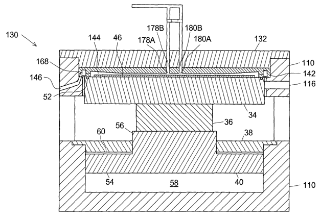
The preferred pressure chamber of the present invention is illustrated in FIG.
9. The
preferred pressure chamber 130 comprises a second pressure chamber frame 110,
a second
top lid 132, the wafer platen 34, the cylinder 36, the sealing plate 38, the
piston 40, and an
upper cavity plate/injection ring 142. The wafer platen 34 and the upper
cavity
plate/injection ring 142 form the preferred wafer cavity 144. The third o-ring
(not shown)
CA 02444296 2003-10-09
WO 02/084709 PCT/US02/11461
located in third o-ring groove 52 seals the preferred wafer cavity 144. The
second pressure
chamber frame 110 comprises an inlet conduit 146. The inlet conduit 146
couples to an
injection ring inlet port 168. A first c-seal (not shown) seals a first
interface between the
inlet conduit 146 and the injection ring inlet port 168. The upper cavity
plate/injection ring
142 comprise third and fourth outlet ports, 178A and 180A, which couple to
fifth and sixth
outlet ports, 178B and 180B of the second top lid 132. Second and third c-
seals (not shown)
seal second and third interfaces between the third and fifth outlet ports,
178A and 178B, and
the fourth and sixth outlet ports, 180A and 180B, respectively.
The upper cavity plate/injection ring 142 of the present invention is further
illustrated
in FIGS. 10A and l OB. The upper cavity plate/injection ring 142 comprises a
second plenum
164, second injection nozzles 166, the injection ring inlet port 168, the
fifth and sixth outlet
ports, 178A and 180A, and a second discontinuous height variation feature. The
second
discontinuous height variation feature comprises a decreasing height feature
170 and. a
uniform height feature 172. The decreasing height feature 170 is located
proximate to an
outer diameter region of the upper cavity plate/injection ring 142. The
uniform height feature
172 is located proximate to an inner diameter region of the upper cavity
plate/injection ring
142.
Preferably, the upper cavity plate/injection ring 142 is fabricated by welding
an outer
ring to a plate. The outer ring comprises the second plenum 164. The plate
comprises the
second injection nozzles 166. Preferably, the outer ring and the plate
comprise 316L
stainless steel.
It will be readily apparent to one skilled in the art that the preferred
pressure chamber
130 and the first and second alternative pressure chambers, 30 and 30B, of the
present
invention are appropriate for high pressure processing that is below
supercritical conditions.
It will be readily apparent to one skilled in the art that other various
modifications
may be made to the preferred embodiment without departing from the spirit and
scope of the
invention as defined by the appended claims.
to