Note: Descriptions are shown in the official language in which they were submitted.
CA 02444385 2003-10-10
WO 02/083570 PCT/USO1/40515
APPARATUS AND METHOD FOR PHOTOCATALYTIC PURIFICATION
AND DISINFECTION OF WATER AND ULTRAPURE WATER
BACKGROUND OF THE INVENTION
Technical Field
The present invention generally relates to a method and apparatus for the
purification
and disinfection of water. More specifically, the present invention relates to
an apparatus and
method of use of a semiconductor material for the photocatalytic degradation
of organic and
inorganic pollutants and microorganisms in water and ultrapure waters. The
present
invention is an apparatus and method incorporating a rigid, three-
dimensionally open celled,
fluid permeable, photocatalytic semiconductor unit.
Background Art
Heterogeneous photocatalysis is the general term that describes the technical
approach, [Mills, A.; Le Hunte, S.; "An Overview of Semiconductor
Photocatalysis," J.
PhotoChem. & PhotoBio. A: Chemistry 108 (1997) 1- 35] and [Hoffman, M.R.;
Martin,
S.T.; Choi, W.; Bahnemann, D.W.; "Environmental Applications of Semiconductor
Photocatalysis," Chem Rev 1995, 95, 69-96]. The specific process is properly
described as
semiconductor-sensitized photomineralization of organics by oxygen. It may be
summarized
as:
Semiconductor
Organic pollutant + OZ ~ C02 + HBO + mineral acid
hV > Ebg
where by represents the energy of a photon and Eb~ is the bandgap energy
separating
electrons in the valence band of the semiconductor from those in its
conduction band.
The process is driven by photons having more energy than the bandgap of the
semiconductor they irradiate. Each such photon absorbed by the semiconductor
will promote
an electron from the valence band producing a conduction band electron (e-)
and a valence
band hole (h+). When the resultant electron-hole pair migrates to the
semiconductor/solution
' Ultrapure water, as used herein, refers to water pre-treated by methods
known to those
skilled in the art to remove suspended and dissolved inorganic and organic
matter.
CA 02444385 2003-10-10
WO 02/083570 PCT/USO1/40515
2
interface, oxidation-reduction processes are initiated. These include;
Holes:
Acidic or neutral solutions: H20 + h+ ~ OH~ + H+
Allcaline solutions: OH- + h+ ~ OH~
Electrons:
Uncertain reaction pathway resulting in the reduction of oxygen to various
reactive species
including:
O~, 02~, OZH~, HOZ-, H202 and OH~.
Of particular importance is the formation of OH~, the hydroxyl radical. The
hydroxyl
r adical is an extremely potent oxidizing agent (redox potential of +2.8 V),
capable of
oxidizing almost all organic compounds. By comparison, the redox potentials
for the more
conventional oxidants chlorine and ozone are +1.36 and +2.07 V, respectively.
Hydroxyl
radicals also kill and breakdown microorganisms and endotoxins.
Semiconductor photocatalysts that have been demonstrated for the destruction
of
organic contaminants in fluid media include but are not limited to: TiOa, ZnO,
CaTi03, Sn02,
Mo03, FezO3, and W03. Ti02 is the most widely investigated because it is
chemically stable,
has a suitable bandgap structure for UV/Visible photoactivation, and is
relatively
inexpensive.
Ti02 exists in two principal crystalline forms: rutile and anatase. The rutile
form of
TiO~ is widely used as a pigment and can be found in almost anything white --
paint, paper,
textiles, inlcs, plastics and cosmetics. Anatase, the low temperature form
(stable below
600°C) is the most photoactive form. Nanoscale (5 - 50 nm) anatase
particles with very high
surface areas (50 - 500 m2/gm) show high photoactivity when irradiated with UV
light (<
390nm) in the presence of water.
The deposition of a transition metal (e.g., platinum, palladium, silver) on
the surface
of the anatase increases the photocatalytic activity by approximately a factor
of two. A
variety of methods improve the quantum efficiency of Ti02 by doping with
various metals to
extend the spectral response into the more efficient visible light
wavelengths, [Borgarello, E.
et aI. "Visible Light Induced Water Cleavage in Colloidal Solutions of
Chromium-Doped
Ti02 Particles," J. Am. Chem. Soc.1982, 104, 2996-3002] or to increase the
minority carrier
diffusion length, [Augustynski, J.; Hinden, J. Stalder, C.; J. Electrochem.
Soc. 1977, 124,
1063] or achieve efficient charge separation to increase carrier lifetimes,
Vogel, R.; Hoyer, P;
CA 02444385 2003-10-10
WO 02/083570 PCT/USO1/40515
3
Welter, H.; "Quantum-Sized PbS, CdS, Ag2S, Sb2S3 and Bi2S3 Particles as
Sensitizers for
Various Nanoporous Wide-Bandgap Semiconductors," J. Phys. Chem. 1994, 98, 3181-
3188].
Most of the early research on semiconductor photocatalysis concerned methods
using
titanium dioxide (Ti02) slurries or TiO~ wash coatings onto or inside a glass
tube and the
photodegradation of organic compounds and their intermediates in water. These
methods of
using Ti02 have limitations for commercial applications. For example, although
Ti02 slurry
has tremendous surface area and has acceptable quantum yields, there are
serious limitations
to the removal of the TiO~ particles from the purified water. While wash
coating Ti02 onto
glass avoids the removal limitations of the slurry approach, it has its own
problems in that
insufficient surface area is presented for effective destruction of organics
within a reasonable
time period. Additionally, the wash coat is not firmly attached to the glass
resulting in a loss
of Ti02 to the water stream and a concomitant reduction in photocatalytic
activity.
Kraeutler and Bard made a photocatalytic reactor of water slurry of suspended
Ti02
powder, in the anatase crystalline form, and studied the decomposition of
saturated
carboxylic acid,[J. ACS 100 (1978) 5985-5992]. Other researchers used UV-
illuminated
slmTies of Ti02 for the photocatalyzed degradation kinetics of organic
pollutants in water.
Mathews created a thin film reactor by wash coating TiOz, (Degussa P25TM),
particles
to the inside of a 7 millimeter long borosilicate glass tube wound into a 65-
turn spiral. The
reactor was illuminated with a 20 watt, black light UV fluorescent tube. He
monitored the
destruction of salicylic acid, phenol, 2-chlorophenol, 4-chlorophenol, benzoic
acid, 2-
naphthol, naphthalene, and florescin in water, [J. Physical Chemistry 91
(1987) 3328-3333].
As an improvement over the prior art approaches, U.S. Pat. No. 4,892,712 to
Robertson et al. disclosed the attachment by the sot-gel process of anatase
Ti02 to a
fiberglass mesh substrate. This mesh was wrapped around a light source
contained within a
quartz glass cylinder and emitting UV radiation in a wavelength range of 340
to 350
nanometers (nm). The entire structure was placed within a stainless steel
cylinder containing
fluid inlet and outlet ports thereby creating a reactor. Polluted water was
passed through this
reactor for purification. Unlilce the present invention, Robertson's mesh is
not rigid, three-
dimensionally open celled and lacks permanent bonding of the semiconductor to
the mesh.
Professor I. R. Bellobono prepared photocatalytic membranes immobilizing 23%
of
Titanium Dioxide (Degussa P-25). Controlled amounts of appropriate monomers
and
polymers, containing the semiconductor to be immobilized and photoinitiated by
a
CA 02444385 2003-10-10
WO 02/083570 PCT/USO1/40515
4
proprietary photocatalytic system was photografted onto a non-woven polyester
tissue. The
final porosity of the photosynthesized membrane was regulated at 2.5-4.0
microns. He trade
named this membrane "Photoperm"TM. A fluid containment structure stuTOUnded
the
membrane creating a reactor. The reactor volume occupied by the fluid was
2.Sliters (1) and
the membrane surface area was 250 linear centimeters (cm2). The reactor was
illuminated
with a cylindrical high-pressure mercury arc lamp at a power of 2 lcilowatts
(1cW) and at a
wavelength of 254nm. Water flowed into the center of the reactor and moved out
tangential
to the lamp through the membrane. This system was used to destroy phenol in
water,
["Effective Membrane Processes. New Perspectives" (R. Paterson, ed.) BHR,
Mech. Eng.
Publ., London (1993), pg 257-274]. The process was patented in Italy in 1995,
Italiaxi Pat.
No. IT1252586. Unlike the present invention, Bellobono's apparatus is not
inert, not three-
dimensionally open celled, and not durable.
Cittenden, et al. discloses a method and apparatus for destroying organic
compounds
in fluids [The 1995 American Society of Mechanical Engineers (ASME)
International Solar
Energy Conference, Maui, Hawaii, USA]. Ti02 was attached by wash coating to a
35x60-
mesh silica gel substrate. The substrate was placed within a plastic tube that
allowed the
penetration of UV light. Organic pollutants in a water stream passed axially
through the
tube. Natural light and/or artificial UV light oxidize the investigated
organic pollutants.
Unlike the present invention, Cittenden's invention is not three-dimensionally
open celled,
not durable, and has very limited fluid pemneability.
Anderson discloses a method to make ceramic titanium membranes by the sol-gel
process. [J. Membrane Science 30 (1988) 243-258]. These membranes are porous
and
transparent to UV illtunination. They are made from a titanium allcoxide and
then fired to
form the anatase crystalline structure. Unlike the present invention,
Anderson's invention is
not open celled, not three-dimensionally reticulated, not durable, and has
very limited fluid
permeability.
Thus, while attempts were made in the prior art to enhance quantum yields by
increasing semiconductor surface area and improving UV light penetration,
serious
limitations remain to the coriunercial development of an efficient, durable
photocatalytic
purification apparatus and method for its use. In Robertson, in addition to
the severe
limitations already above noted, the flexible strands of fiberglass precluded
the permanent
attachment of Ti02 because, as water passed by, the fiberglass strands bent
and flexed
CA 02444385 2003-10-10
WO 02/083570 PCT/USO1/40515
releasing TiOz particles, particularly at high fluid flow rates. For
Bellobono, in addition to
all the limitations also above noted, the photocatalytic process gradually
oxidized the organic
membrane reducing its activity over time. In addition to all the limitations
also above noted,
Cittenden's Ti02 sloughed-off because it was wash coated to the silica gel
substrate. In
5 addition, the void space between silica particles was so small that flow
through the system
was restricted malting the structure unsuitable for commercial applications.
In Andersen's
membrane, in addition to the limitations above noted, limitations on the
structural integrity of
these membranes exist particularly at high fluid velocities needed for
efficient industrial
applications.
Disclosure of Invention
The object of the present invention is to substantially improve upon the prior
art to
produce an effective, quantum efficient, durable, economic, commercial
apparatus for the
rapid photocatalytic purification and disinfection of water and ultrapure
water. At the present
time in the semiconductor processing industry, current technology struggles to
achieve 2
parts-per-billion (ppb) in Total Organic Carbon (TOC). This represents a limit
on the
industry's ability to achieve further improvements in the chip density and
speed. The present
invention, which achieves 500 parts-per-trillion (ppt) in TOC, or better,
represents a
breakthrough for both the water purification and semiconductor industry. The
invention also
has profound implications for other water purification systems, including
those related to
environmental cleanup.
The apparatus of the present invention involves a reactor apparatus and a
method for
its use for photo-promoted, catalyzed degradation of compounds in a fluid
stream. The
effectiveness of the process is determined in part by the mass transfer
efficiency, which is the
rate at which the contaminant is transported from the fluid stream to the
photocatalytic
surface where it can be destroyed. Mass transfer is greatly aided by
proximity. The
photocatalyst is widely and uniformly distributed in the volume of water to be
treated, such
that a contaminant is never far from a catalyst surface
Another feature of the present invention is the uniform illumination of the
catalyst
within the vohune of water to be treated. Since the catalyst itself absorbs
the light, its
concentration in the volume is limited to allow sufficient penetration of the
activating
photons. In addition, in the preferred embodiments, the support structure does
not block
CA 02444385 2003-10-10
WO 02/083570 PCT/USO1/40515
6
illumination of the volume of water to be treated. Thus, the volume fraction
of support
material is minimized andlor has high transparency to the activating photons.
To enhance
volumetric illumination, in an embodiment which employs a substrate, the
substrate material
is preferably made from glass or other materials transparent or
semitransparent to the
photoactivating wavelengths between 180nm and 700nm. This is possible using a
rigid,
three-dimensionally open celled photocatalytic semiconductor unit. In an
embodiment which
bonds or chemically integrates the substrate with the semiconductor, the unit
is also
preferably made from transparent or semitransparent materials.
The water flow through the catalyst is turbulent to improve mixing and mass
transfer
rates between the organic contaminants and the oxidizing species generated at
the catalyst
surface. Laminar flow is largely avoided.
The open celled structure utilized in a first preferred embodiment of the
present
invention substantially represents a breakthrough over the prior art and
allows for the
commercial use of photocatalytic technology in ultrapure water production
because it
optimizes mass transfer, surface area, illumination, water flow, durability,
rigidity, and so
forth. The photocatalytic semiconductor unit provides a high surface area,
rigid structure on
which the photocatalyst is deposited or into which it is incorporated. The
interstitial struts
forming the open celled structure of the photocatalytic semiconductor unit are
relatively thin,
so volume fraction of substrate support material is low and flow is not
significantly
restricted. The ramification and alignment of the struts with respect to the
flow direction will
generate tortuous flow paths and enhance mass transport. The rigidity of the
support
structure provides a stable base to permanently attach or incorporate a highly
active Ti02
surface.
Brief Description of the Drawings
FIG. 1 is a partial cross-sectional side view in elevation showing a first
preferred
embodiment of a point-of use reactor with LED's as the source of
photoactivating light.
FIG. 2A is a partial cross-sectional side view in elevation of a cylindrical
tube reactor
in which water flows in and passes radially through the open celled
photocatalytic substrate
and axially past the UV light source;
FIG. 2B is a cross-sectional end view of the reactor of FIG. 2A;
FIG. 3 is a schematic drawing of a purification system that includes an air
injection
CA 02444385 2003-10-10
WO 02/083570 PCT/USO1/40515
7
system for injecting gas into the water before it is introduced into the
photocatalytic system;
FIG. 4 is a view showing detail of the open celled photocatalytic
semiconductor unit
of the first preferred embodiment of the present invention;
FIG. 5 is a partial cross-sectional perspective view of a reactor tube having
an
alternative semiconductor unit substrate structure;
FIG. 5A is a partial cross-sectional side view in elevation showing detail of
the
surface topography of the substrate structl~re shown in FIG. 5;
FIG. 6 is a schematic drawing of an experimental test system used to evaluate
the
performance of the present invention;
FIG. 7 shows the results of a flow rate optimization study;
FIG. 8 shows the comparison of the photocatalytic destruction of acetic acid
over
time for a fiberglass mat substrate and a three-dimensionally open celled
photocatalytic
semiconductor unit utilized in an embodiment of the present invention; and
FIG. 9 shows a comparison of the photocatalytic destruction of acetic acid
over time
for LTV photolysing/mixed bed ion exchange system compared to the LJV
photolysing/mixed
bed ion exchange plus an open celled semiconductor unit:
Best Mode for Carrying Out the Invention
The present invention is directed to the use of a photocatalytic semiconductor
unit
photo-actively charged with a semiconductor for use in a reactor apparatus and
method for
the purification and disinfection of water for the semiconductor industry,
environmental
cleanup, and for the home point-of use market.
In a first preferred embodiment, the present invention discloses an apparatus
and
method for purifying water and ultrapure water that solves problems of the
prior art by
transporting water through a rigid, three dimensionally open-cell material
characterized by an
inert, porous, photoactivating light semitransparent, fluid permeable, high
surface area
substrate onto which a photocatalytic semiconductor layer is permanently
bonded, into which
it is incorporated, or of which it is fabricated. The material described in
the present invention
and the apparatus and method for its use in photocatalytic purification and
disinfection of
water and ultrapure water is further characterized by high contact efFciency
turbulent fluid
flow with relatively low pressure drop. In a second and third preferred
embodiment, the
photocatalytic substrate is not open celled but nonetheless presents a large
surface area over
CA 02444385 2003-10-10
WO 02/083570 PCT/USO1/40515
8
which the water flows and that also induces turbulent flow of the water
through the system.
It will be readily appreciated by those skilled in the art that the current
invention can
be used to purify water in manufacturing semiconductors and pharmaceuticals,
in
biotechnology, power plant water, bottled water, municipal water supplies,
point-of use, to
name just a few examples.
Although never before used for the present purpose, three dimensionally open-
cell
substrates made from a variety'of materials are scientifically described and
commercially
available. Such materials, all of which may be suitable for use in the present
invention,
include alumina, titania, aluminum, gold, copper, metal alloys, carbon,
silica, glass, quartz,
organic polymers, silicon carbide, silicon nitride, boron nitride, zirconium,
tungsten carbide,
and many more. One of many methods of making an open celled substrate is
described in the
prior art - U.S Pat No. 3,052,967 to Fischer; 3,946,039 to Walz; 4,568,595 to
Morris; and
5,441,919 to Park et al. Custom substrates may also be made utilizing the
stereolithograhic
process or selective laser sintering or other methods familiar to those
experienced in the art.
The rigid, three-dimensionally open celled substrate utilized in a first
preferred embodiment
of the cL~rrent invention possesses a highly variable surface, with an easily
controlled surface
roughness and a huge macro surface area, depending on the overall pore size
from
approximately 4 to 96 pores per linear centimeter (ppc), approximately 10 to
240 pores per
linear inch (ppi). The concentrated yet compact surface area opens the
possibility of using a
great variety of attachment methods; such as, without being limited to, sol-
gel process, ion
assisted gun deposition ion beam sputtering, chemical vapor deposition,
aerosol application,
evaporation deposition, etc.
Literature and the prior art explain the procedures necessary for the
permanent
bonding of Ti02 to a substrate. For example for sol-gel process refer to: U.S.
Pat. No.
4,892,712 to Robertson; U.S. Pat. No. 6,013,372 to Hayalcawa , et al., and
U.S. Pat. No.
6,093,676 to Heller, et al., or in literature, Preparation, Microstructure and
Photocatalytic
Activity of Porous Ti02 Anatase Coatings by sol-gel Processing, [J Sol-Gel
Science and
Technology 17 (2000) 163-171] by Jiaguo Yu, et al; Nanocrystallite Titanium
Dioxide Films
Made by the Sol-Gel Method Using Reverse Micelles, [J Sol-Gel Science and
Technology 10
(1997) 83-89] by E. Stathaios, et al. For chemical vapor refer to: U.S. Pat.
No. 5,389,401 to
Gordon, or in Metal Organic CVD of Nanostructured Composite Ti02-Pt Thin
Films: A
Kinetic Approach, [Chern. Vapor Deposition 5 (1999) 13-20] by Giovanni, et al.
Yet another
CA 02444385 2003-10-10
WO 02/083570 PCT/USO1/40515
9
method condenses from aerosolized semiconductor droplets, as described in
Deposition of
Multifunctional Titania,Films by Aerosol Routes, [J. Am. Ceramic Soc. 82
(1999) 10] by G.
Yang and Pratim Biswas. While these are some of the popular methods for
attaching
semiconductor films, we do not limit ourselves to variations on them and other
methods that
are to be found in prior art.
The semiconductor layer may also be formed chemically in situ by oxidation of
the
underlying metal, either electrochemically or thermally or by chemical
reaction. See for
example Titanium Dioxide Film Electrodes Prepared by Thermal Oxidation, [J.
Electrochem.
Soc. 139, no. 7, (1992) 1803 by Choi Yong-lcoolc et. al. and In Situ Raman
Spectra of
Anodically Formed Titanilun Dioxide Layers in Solutions of H2S04, I~OH and
HN03, [J.
Electrochem. Soc. 138 no. 10 (1991) 2964].
In a further embodiment the substrate is made of the same material as the
semiconductor layer and the two materials are chemically integrated. This
creates stable
surface capable of withstanding tremendous t<ubulent flow.
Photocatalytic activity of many semiconductor surfaces is enhanced by a
process of
doping or coating these surfaces with a variety of metals, including
transition metals such as,
but not limited to, platinum, palladium, ruthenium, iridium, rhodium, gold,
silver, copper, tin,
iron, cobalt, vanadium, niobium, and zinc. Combinations of these metals and
their oxides,
sulfides or other compounds are known to those experienced in these arts. By
altering the
doping of Ti02 the band gap energy can be shifted to the visible spectrum
(400nm-700nm).
Zang. et al. showed that the addition of platinum (IV) halide shifted the band
gap energy
required for TiO2 from 335nm to 366mn to 400rim into the visible spectrum.
[Amorphous
Microporous Titania Modified Platinum (IV) Chloride - A New Type of Hybrid
Photocatalyst
for Visible Light Detoxification. J Phys. Chem. B 102 (1998) 10765-10771].
Doping with
iron or chromium produces similar results. [Visible Light Induced Water
Cleavage in
Colloidal Solutions of Chromitun-doped Titanium Dioxide Particles. J ACS 104
(1982) 2996-
3002, by E. Borgarello, et al.]
An enhancement of the preferred embodiment is a film made from the anatase
form of
Ti02 in a usable grain size for particles from 1 to 30 nanometers in diameter.
An active
surface thickness can vary from 1 to 190 micrometers. Platinum was found to be
effective
dopant to increase activity when applied in the range of from 0.025 to 3% by
weight of the
titanium dioxide, though a range of 0.05 to 1 % may be optimal. Platinum as
specified above
CA 02444385 2003-10-10
WO 02/083570 PCT/USO1/40515
increased the TOC destruction activity by a factor of 2 to 3. A further
enhancement of the
dopant is a vanadium compound, such as vanadium pentoxide (0.1 to 15% by
weight of the
Ti02) on a semiconductor such as Ti02, when used in combination with ozone. It
increases
the rate of destruction of TOC by a factor of 2-8 times. This enhancement
applies in the dark
5 as well as under illumination. This means that if light does not penetrate
to the interior of the
substrate, TOC will still be destroyed.
A further enhancement of the first preferred embodiment of the apparatus and
method
of the present invention consists using a combination or set of open celled
substrates, each
with its own particular variety of parameters and enhancements and each
designed to operate
10 on a particular component of the TOC. For instance, one set may work on
polar/non-polar
components, while others work on hydrophobic/ hydrophilic components,
aromatic/aliphatic
components, alcoholic/acidic components and chemical/biological components.
The members
of the set are used in a series combination where water flows thru first one
member and then
another member. This enhancement enlarges the scope of the invention by
bringing a
complete collection of destruction capabilities to bear on combinations of
contaminants, even
though individual members of the set are alone incapable of achieving
acceptable overall TOC
destruction levels.
Preferred light sources include, without being limited to low, medium and high-
pressure mercury lamps, xenon lamps, and conventional and ultraviolet emitting
LED's, or
any other light source that activates the semiconductor by producing light at
a wavelength of
between 180 to 700 nm.
Drawing attention to U.S. Pat No. 5,116,582, to Cooper, et al. entitled
Photocatalytic
Slurry Reactor Having Turbulence Generating Means, the creation of turbulence
has been
recognized in prior art as a necessary condition for effective TOC
destruction. Effective TOC
destniction requires that organic molecules present in the water come into
close proximity to
the active surface. The open celled photocatalytic semiconductor unit, and the
alternative
substrate structures described for use in the apparatus and method of the
present invention,
behave superbly in this regard. Each cause turbulent water flow, and the open
celled
photocatalytic semiconductor wit, in particular, causes dramatically turbulent
water flow,
causing the water flowing through its pores to shear, thrashing from side to
side within the
pores, and to speed up and slow down according to the cross section of the
pore openings.
Further, it causes microturbulence within the pores themselves. Open celled
photocatalytic
CA 02444385 2003-10-10
WO 02/083570 PCT/USO1/40515
11
semiconductor units provide many ways to control turbulence by adjusting pores
sizes and
pore distributions, pore wall formations and surface textures.
As a further enhancement of the invention, known methods exist to grade the
size of
the poxes so that they start large near the surface at approximately 4 ppc
(~10 ppi), and then
diminish in size towards the photocatalytic semiconductor unit interior at
approximately 96
ppc 0240 ppi), thus providing tailored light guides. Additionally, the water
itself may be
modified such as by adding microscopic gas bubbles (such as gaseous oxygen,
ozone, or
peroxides) to guide the light into the interior. The materials of construction
of the
photocatalytic semiconductor unit can be varied from reflective (metals) to
opaque (TiOa,
carbon, metals) to transparent (silica, alumina) to provide further control
over the penetration
of the photoactivating light. Innovative designs can incorporate light guides
including, but not
limited to, light fibers, quartz blocks, voids, gaps and separations.
Although particular embodiments of the present invention have been described
and
illustrated herein, it should be recognized that modifications and variations
might readily
occur to those skilled in the art and that such modifications and variations
may be made
without departing from the spirit and scope of our invention. Consequently,
our invention as
claimed may be practiced otherwise than as specifically described.
Referring now to Figs. 1-10, wherein like reference numerals refer to like
components
in the various views, FIG. 1 shows an example of a point-of use reactor 10
with LED's 12 as
the photoactivating light. Contaminated source water flows into the reactor
housing 14
through inlet 16. The water then flows through the open celled semiconductor
unit 18 that is
photoactivated by LED's 12. A support/wiring plate 20 holds the LED lights. A
transparent
plate 22 is provided to isolate the LED lights from the water flow. Purified
water exits the
reactor through outlet 24. The point-of use reactor housingl4 can be
constructed from a
variety of thermoplastics (polyproplylene, etc), or metals (304 stainless
steel, 316 stainless
steel, etc), or other materials that are both inert to degradation by the LED
light source and
resistant to corrosion by water. Further, the enclosure may either be integral
with the
semiconductor unit or separable, the latter configuration preferable in cases
where the removal
and installation of a replaceable semiconductor unit is desired. The
semiconductor unit
defines a fluid passage 26 in fluid communication with inlet 16 and outlet 24.
The point-of use reactor can use an open celled semiconductor unit 'that is
photoactivated by LED's that emit UV energy at 390 nm or lower. The point-of
use reactor
CA 02444385 2003-10-10
WO 02/083570 PCT/USO1/40515
12
can also use an open celled semiconductor unit that is doped to shift the band
gap to visible
wavelengths. In this reactor, an LED that emits visible wavelengths is
utilized. This latter
configuration enables a more efficient use of the LED energy.
The point-of use reactor is designed to be commercialized into markets defined
by low
and intermittent demand for purified water, such as potable water in the home.
This reactor is
superior to existing technologies because it uses only a small percentage of
energy and it does
not transmit heat to the product water while not in use (eliminating the need
to rinse the
system to ambient temperature prior to using product water). In addition, the
reactor only
requires low power electrical energy per LED, making it both safe for the user
in an
environment that includes water and electricity and enabling the reactor to be
utilized in
portable applications (e.g., battery or solar powered).
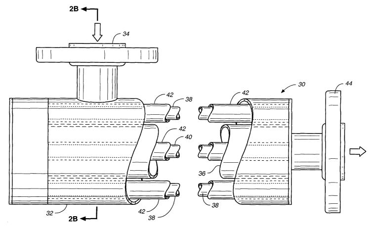
FIG. 2A is a partial cross-sectional side view in elevation of a cylindrical
tube reactor
30, suitable for commercial/industrial applications, having a generally
elongate housing 32
into which water flows through inlet 34 and then passes radially through the
open celled
photocatalytic unit 36 and axially past a IJV light source comprising tube
type lamps 38 and
40 as the photoactivating light. FIG. 2B is an end view of the same
commercial/industrial
reactor 30. The open celled photocatalytic semiconductor unit 36 is a
cylinder. Both the
exterior photoactivating lights 38 and interior photoactivating lights 40 are
tubes enclosed by
cylindrical quartz sleeves 42. After contaminated source water flows into the
reactor through
inlet 34, it flows radially through the open celled semiconductor unit and
passes by the
exterior the photoactivating lights. The contaminated water flows axially
through the reactor,
through the substrate and over the photoactive surface, where the
photoreactive surface is
activated by both the exterior photoactivating lights and by the interior
photoactivating lights.
Purified water flows out through outlet 44.
The commercial/industrial reactor is designed to be commercialized into
marleets
defined by high and continuous demand for pl~rified water. The configuration
of the reactor is
designed to be modular so that longer and/or parallel reactors can be employed
for higher
flows. Series reactors with different sets of open celled photocatalytic
semiconductor unit
specifications and/or different wavelengths for the exterior and interior
photoactivating lights
can be employed for custom purification of source water with different
polar/non-polar
components, hydrophobic/hydrophilic components, aromatic/ahiphatic components,
ahcoholic/acidic components, and chemical/biological components.
CA 02444385 2003-10-10
WO 02/083570 PCT/USO1/40515
13
FIG. 3 is a schematic drawing of a water purification system 50 that includes
a gas
injection system 52 for injecting gaseous oxygen, ozone, or peroxides, and
thereby modifying
the water to facilitate the passage of light into the interior of the
semiconductor unit. The gas
injection system includes a gas supply, tank, or reservoir 54 in fluid
communication with a
mixing chamber 56 through a gas line 58. The mixing chamber is 'preferably a
venturi.
Interposed between the gas tank and the mixing chamber are one or more flow
control valves
60 for regulating the gas flow into the mixing chamber, where it is injected
into water flowing
into the chamber. After gas is introduced into the water, the water is then
processed in the
photocatalytic system 62 as described above.
FIG. 4 is a sectional view showing detail of an open celled photocatalytic
semiconductor unit 70. The unit includes a plurality of differentially sized
pores 72, with pore
sizes ranging from 4 to 96 ppc (~10 to 240 ppi).
FIG. 5 is a partial cross-sectional perspective view of a reactor tube having
an
alternative semiconductor unit substrate structure. In this embodiment, the
photocatalytic
system 80 includes a reactor housing 82 having a water inlet end 84 and an
outlet end 86.
Running axially substantially the entire length of the housing are a plurality
of tube-type lights
88 encased.within quartz sleeves 90. Water flows into the housing and over a
substrate 92
having a large surface area 94. Unlike the open celled semiconductor unit of
the first
embodiment, wherein water flows through the semiconductor unit structure, the
semiconductor unit of this embodiment promotes fluid flow over and around the
photoactive
surface area. The principle of action, however, remains the same, as the
substrate is coated or
impregnated with a catalyst that promotes hydroxyl radical migration to the
surface of the
substrate when exposed to light of selected wavelengths. Contaminant molecules
exposed to
the surface are thus oxidized.
It will be recognized that there are inmunerable possible configurations of
the
semiconductor substrate. However, as a general rule it is most advantageous to
provide a
geometry that induces turbulent fluid flow over the substrate surface as well
as providing a
maximum surface area. Such configurations may include, for example, a helical
screw
substrate 92 surrounding an axially disposed rod 96, as shown. To maximize the
surface area
of the substrate, it is preferable to include surface contours or topography
98, including
bumps, protrusions, corrugations, ridges, fins, flanges, mesh, three-
dimensional matrices, as
shown in Fig. 5A. The thrust of the surface features is to enhance turbulent
flow by creating
CA 02444385 2003-10-10
WO 02/083570 PCT/USO1/40515
14
counter-rotating vortices, cross-current mixing, division and recombination of
water, and
otherwise mixing and agitating the water stream.
FIG. 6 is a schematic drawing of a laboratory water purification system 120
utilized in
evaluating the present invention. The water system utilized for laboratory
testing is configured
t~ provide the flexibility required for a wide range of laboratory
experiments. The exact
volume of the water system is carefully measured. The feedwater for any
experiment is added
through a covered storage tank 122. Feedwater can range from typical point-of
use water to
ultrapure water. An exact amount of organic impurities is also added through
the storage
taut. Since the water volume of the system is precisely known, the level of
organics in an
experiment can be mixed to a predetermined level and verified with the TOC
analyzer 134.
The system includes a pump 124, a rotometer 126, a throttling valve 128 to
control
system flow, an ultraviolet (UV) photolysing unt 130 with 185/254 nm UV lamps,
a test
chamber with a photocatalytic surface 132, a TOC analyzer 134, and a mixed bed
ion
exchange (MBIX) unit 136. Valves 138 are provided to isolate the UV
photolysing unit 130;
Valves 140 isolate the test cell and the test chamber 132; valves 142 isolate
the MBIX unit;
and shunt valves 143a-c allow the photolysing unit130, the TOC analyzer 134,
and the MBIX
unit 136 to be selectively bypassed, either individually or in any
combination. The TOC
analyzer 134 measures TOC, temperature, and resistivity. The water from the
TOC analyzer
can be returned to the storage tank, or the same stream can be diverted to
drain from the TOC
analyzer if desired.
The system enables testing of variables including, but not limited to
feedwater water
quality (including analysis, conductivity, temperature), feedwater TOC, system
flow rate,
choice of applying either 185/254 nm, 254 nm UV energy or no light energy at
all, choice of
applying the MBIX unit (including the choice of resins installed), a choice of
the TOC
analyzer utilized, the choice of the light source utilized to illuminate the
photocatalytic surface
(including wavelength, power, and the option to illuminate from multiple
locations including
180 degrees), the choice to add microbubbles in the feedwater to the
photocatalytic surface,
and all of the possible choices and variations associated with the
photocatalytic surface,
including, but not limited to, material, surface preparation, surface coating,
doping, size of
pores, pore dispersion matrix, thickness of the ligaments, and the thickness
of the
photocatalytic surface.
CA 02444385 2003-10-10
WO 02/083570 PCT/USO1/40515
EXAMPLES:
EXAMPLE 1 - Fig. 7 depicts TOC removal rate as a function of flow rate. The
rigid 3-
dimensional open celled semiconductor unit (99.5% alumina, 45 ppi, 1.5 inches
in diameter by
5 0.50 inches thick) coated with a 2:1 mixture of alumina sol and 35 11m
particle Ti02 in the
anatase form was placed in the photocatalytic reactor of the test loop of FIG.
6. Acetic acid
was spiked through the tank 122 and the flow was adjusted with valve 128 and
monitored with
flow meter 126. The photocatalytic substrate was illuminated with 365 nm light
at 3
milliwatts/cm2. The water was shunted past the ultraviolet (LTV) photolysing
unit 130 and
10 MBIX unit 136 and passed through the photocatalytic reactor cell 132 which
contains the
photocatalytic semiconductor unit. The rate of oxidation of the acetic acid
was monitored with
a TOC analyzer 134 over time comparing two different flow rates. First order
rates are
compared among the different surfaces that have been tested to create a useful
ranking of
different surfaces and geometries. The first order rates are found to be
significantly dependent
15 on flow rates, which is related to the degree of turbulence and mixing that
occurs. It is clear
from FIG. 7. that peak effectiveness in this sample is found at a flow rate of
0.8 gpm with
14.3% TOC reduction in one hour compared to 9.2% TOC reduction at 0.5 gpm.
EXAMPLE 2 - FIG. 8 compares the performance of a prior art substrate and the
open celled
semiconductor unit utilized in the present invention. It uses the same water
loop configl~ration
of FIG. 6. That is the water is shunted by the ultraviolet (IJV) photolysing
unit 130 and the
MBIX unit 136. The photocatalytic surfaces compared are fused silica (20 ppi,
1.5 inches in
diameter by 0.25 inches thick) and fiberglass mat. Ti02 in the anatase form
was deposited via
sol gel techniques to the fused silica and the fiberglass mat. Both samples
were platinum
doped. Water was passed through the open celled fused silica and fiberglass
mat at 1 gallon
per minute (gpm) and illuminated at 3milliwatts/crnz at 365 nm wavelength. The
water was
spiked with 100 ppb acetic acid. The water was monitored with a TOC analyzer.
Each
photocatalytic semiconductor unit is independently evaluated according to the
previously
described procedures and the data was graphed.
FIG. 8 compares the fiberglass mat substrate to the fused silica open celled
semiconductor unit. The open celled fused silica underwent 57% mineralization
in 13 minutes
while fiberglass mat had 11% mineralization in 13 minutes. Turbulent flow of
water through
the open celled semiconductor unit utilized in the present invention explains
the better results.
Even though the fiberglass mat is semitransparent to ITV light and has more
surface area than
CA 02444385 2003-10-10
WO 02/083570 PCT/USO1/40515
16
the open celled photocatalytic semiconductor unit, it does not induce or
enhance turbulent
mixing.
In "Guidelines for Ultrapure Water in Semiconductor Processing"( Sematech
Co~sortizem, National Technology Roadn2ap for Semiconductors: Technology
Needs, 1997 Ed.,
p. 170)and the "Standard Guide for Ultrapure Water in the Electronics and
Semiconductor
Industry"( ASTlIl Standard D5127-98, 'Standard Gzcide for Ultrapure Water Used
in the
Electrov~ics and Semiconductor Industry, Tlol. 1l. 02) water purity level is
related to process
line width. For line widths >0.5 microns total organic concentration (TOC)
levels of < 2.0 ppb
are recommended. For line widths in the range 0.35 - 0.18 microns recommended
TOC levels
are below 1 ppb. Current technology struggles to achieve the 2 ppb level and
has not come
close to achieving the 1 ppb level. The International Road Map for
Semiconductors shows the
following schedule for achieving these water purity goals:
Year: 2000 2001 2002 2003 2004 2005
Max. TOC Level: 2ppb 2 ppb lppb lppb <lppb <lppb <lppb
Current ultrapure water treatment systems utilize carbon and multimedia
adsorption
beds, various filtration units, reverse osmosis, and ion exchange membranes to
remove
inorganic contaminants and reduce TOC levels to the 10 - 20 ppb range. To
bring TOCs down
further, photolysing is used. This process requires deep UV irradiation (185nm
and 254nm)
using massed banks of UV lamps to decompose organics in water. The process is
terribly
inefficient, but is the only technology available to bring organic
contamination down to
marginally acceptable levels of 2 - 5 ppb. A common experience in the
semiconductor
industry is that at these levels, photolysing reaches a barrier at which point
the curve of TOC
versus total expended energy flattens out. This barrier, evidently, is due to
one or more
molecules present in low concentrations that are particularly difficult to
destroy by
photolysing.
EXAMPLE 3 - In FIG. 9 water in laboratory water purification system 120 of
FIG. 6 was
spiked with acetic acid (10 ppb) through tank 122 and passed through an
ultraviolet (UV)
photolysing unit 130 and then a test chamber with a photocatalytic surface 132
utilized in the
present invention and then through the MBIX unit 136 and monitored with a TOC
analyzer
134. The test chamber with a photocatalytic surface 132 was illuminated with a
365nm (3
CA 02444385 2003-10-10
WO 02/083570 PCT/USO1/40515
17
mW/cm2) light. The flow was 0.7 gpm.
FIG. 9 shows the results. First the destruction of acetic acid was evaluated
with the
ultraviolet (LTV) photolysing mut 130 and the MB1X unit 136 in operation. Next
the
destruction of acetic acid was evaluated with the same configuration plus a
test chamber with a
photocatalytic surface 132 containing the open celled semiconductor unit
utilized in the present
invention. With the ultraviolet (LTV) photolysing unit 130 and the MBIX unit
136 in operation,
the water reached a steady state barrier around 1.5 ppb TOC and then started
to climb. While
TOC in the water passing through the ultraviolet (LTV) photolysing unit 130
and the MBIX unit
136 in operation plus the photocatalytic open celled reactor with good light
penetration,
turbulent flow, and high surface area was reduced to 0.50 ppb.
The essential method of using the above-described apparatus for photocatalytic
degradation of organic, inorganic, and microbiological contaminants in a fluid
stream, involves
the following steps: (1) providing a reactor enclosure having a water inlet
and a water outlet;
providing at least one semiconductor unit, disposed within the reactor
enclosure and interposed
between, and in fluid communication with, the water inlet and the water
outlet, and with which
the fluid stream comes into contact, wherein the semiconductor unit includes a
substrate having
a photoreactive semiconductor surface fabricated of semiconductor material;
(2) providing a
light emitting means in optical proximity to the semiconductor surface for
promoting electrons
from the valance band to the conduction band of the semiconductor material;
and (3) directing
a fluid stream over the semiconductor surface while engaging the light
emitting means to
photactivate the semiconductor surface, whereby contaminants are removed from
the fluid
stream by photocatalytic reaction.