Note: Descriptions are shown in the official language in which they were submitted.
CA 02444517 2003-10-21
WO 03/073061 PCT/US03/05356
METHOD AND SYSTEM FOR INSPECTING OPTICAL DEVICES
Related Application
This application claims priority from a provisional application U.S. Ser.
No. 60/359,074, filed on February 21, 2003, and entitled "Method and System
For Inspecting Optical Devices."
Field of the Invention
This invention generally relates to inspecting optical devices or media,
such as ophthalmic lenses. More specifically, the invention relates to such
systems for automatically inspecting optical devices and to techniques and
procedures that are well suited for use in such systems.
Over the last several years, automated techniques have been
successfully developed for inspecting ophthalmic lenses, particularly contact
lenses. Such techniques are disclosed, for example, in U.S. Patent 5,500,732
and U.S. Patent Application Serial No. 09/751,875, filed December 29, 2001.
Generally, in these techniques, radiation, which may be ultraviolet light,
visible light, or a laser, is directed through a lens to form an image of the
lens
on a pixel array. Digital data values are produced that represent the
intensity
of the radiation on the pixels of the array, and a computer is used to process
those data values to determine if the lens has any unacceptable flaws or
defects. Any lens that has such a flaw or defect is then identified and
rejected.
Many of these techniques are very effective at insuring that any lens
that has an unacceptable flaw or defect is rejected. At the same time, these
techniques sometimes reject acceptable lenses, a result referred to as false
rejects. One reason for this is that many of the procedures are not able to
distinguish between certain types of lens defects and other features that may
appear on the pixel array but which are not lens defects.
When an inspection system detects a feature on the pixel array but
cannot determine whether that feature is a lens defect or another
indistinguishable but acceptable feature, the lens is rejected. For instance,
with several inspection techniques, the lenses are inspected while submerged
in a liquid solution, and it is very difficult to distinguish between holes in
a lens
1
CA 02444517 2003-10-21
WO 03/073061 PCT/US03/05356
(which are unacceptable) and bubbles in that liquid solution (which are not a
lens defect). As a result, acceptable lenses may be rejected because of
bubbles in the liquid solution.
As another example, with prior art automated lens inspection systems,
it is very difficult to distinguish between molded contact lenses that have
tears
or holes and molded contact lenses that simply have been slightly pulled
away from a mold section. To elaborate, contact lenses may be made, for
example as disclosed in U.S. Patent 5,540,410, by molding a suitable polymer
between two plastic mold sections. After the polymer partially hardens, one of
the mold sections is pulled away from the other mold section to provide
access to the lens.
In this process, as a lens is made, holes or tears may develop in the
lens. Also, as the mold sections are pulled apart, a lens may become
delaminated - that is, the edge of the lens may pull away slightly from the
mold section in which the lens remains. It is very difficult for an automated
inspection system to distinguish between a lens that has just slightly pulled
away from the mold section (which is not a lens defect), and a lens that has a
hole or is torn (which is a lens defect). Because of this, acceptable lenses
may be rejected.
Brief Description of the Drawings
Figure 1 is a block diagram generally illustrating a lens inspection
system that may be used in the practice of the present invention.
Figure 2 shows portions of the illuminating and imaging subsystems of
the inspection system shown in Figure 1.
Figure 3 shows spectral bands that may be used to illuminate a lens in
the system of Figures 1 and 2.
Figure 4 shows a lens image made in the system of Figures 1 and 2
and using a first spectral masking technique.
2
CA 02444517 2003-10-21
WO 03/073061 PCT/US03/05356
Figure 5 is a flow chart for a preferred procedure for analyzing a lens
image made using the first spectral masking technique.
Figures 6 and 7, which are similar to Figures 1 and 2 respectively,
show a second lens inspection system that also may be used in the practice
of this invention.
Figure 8 illustrates filter elements that may be used to provide a
second spectral masking technique, which may be used to illuminate a lens in
the inspection system of Figures 6 and 7.
Figure 9 shows a lens image made using the second spectral masking
technique.
Objectives of the Invention
An object of this invention is to improve systems for inspecting optical
devices. Another object of the present invention is to reduce the percentage
of false rejects in an automated lens inspection system.
A further object of the invention is to provide an automated system for
inspecting optical devices that is able to identify certain features more
accurately. A further object of the invention is to provide an automated lens
inspection system having an improved ability to distinguish between holes in
the lenses and bubbles in liquid solutions in which the lenses are submerged.
Another object of this invention is to illuminate a lens that is submerged
in a liquid, in a way that facilitates distinguishing between holes in the
lens
and bubbles in the liquid. A further object of the invention is to provide an
image analysis technique that can distinguish between images of a hole in an
ophthalmic lens and images of bubbles in a liquid in which the lens is
submerged. Another object of this invention is to illuminate a lens in such a
way that delamination of the lens is not shown, while hole and tears in the
lens are shown.
3
CA 02444517 2003-10-21
WO 03/073061 PCT/US03/05356
A further object of the present invention is to provide an illumination
technique, referred to as spectral masking, that illuminates objects with
light in
different, separate wavelength bands. Alternatively, the object may be
illuminated by light comprising the separate wavelength bands and additional
bands; however, the imaging system is sensitive to only the separate
wavelength bands, or the wavelengths of light that are not desired are
filtered
out prior to the imaging system. Another objects of this invention is to
provide
spectral masking techniques that may be used to enable a lens inspection
system to identify certain features more accurately.
A further object of the present invention is to illuminate different
portions of an optical device with different wavelength bands. Still another
object of the invention is to illuminate a central portion of a molded contact
lens in a way that shows whether holes or tears are present in that portion of
the lens, without illuminating outer portions of the lens in the same way.
These and other objectives may be attained with the inspection and
analysis procedures disclosed herein. Generally, these procedures employ,
or are used with, a unique illumination technique, referred to as spectral
masking, in which an optical device is illuminated with plural wavelength
bands. With one spectral masking technique, the entire optical device is
illuminated with two separate bands, which may be part of a continuous
spectrum of light; and in another spectral masking technique, different
regions
of the optical device are illuminated with different bands. The former
technique may be used to differentiate between bubbles in solution and holes
in the optical device, which is particularly well-suited for analyzing lenses
in
solution in a package; however, the technique may also be used to find holes
in a lens in a mold piece. This invention is useful in inspecting very thick
lenses, e.g. -6 lenses or higher that are too thick to be analyzed using a uv
inspection method alone. The spectral masking technique that illuminates the
optical device with different bands at different regions of the device is
particularly well-suited for analyzing contact lenses in a mold piece and may
be used to avoid rejecting acceptable lenses simply because they are
delaminated.
4
CA 02444517 2003-10-21
WO 03/073061 PCT/US03/05356
More specifically, in accordance with a first aspect of the invention, a
method and system are provided for imaging an optical device such as an
ophthalmic lens. In the image formed with this procedure, images of bubbles
and holes have discernible differences. This method is a plural-spectral
imaging/inspection method for an object whereas the object has varied
spectral absorption levels comprising at least one illumination source
comprising wavelengths that are at least partially absorbed, preferably mostly
absorbed and wavelengths that are at least partially transmitted, preferably
most transmitted by the object to produce a partially translucent image.
With the preferred embodiment, the technique relies on the ultraviolet
absorption qualities of an ultraviolet inhibitor in the lens to create the
desired
translucent/shaded effect. The effect is achieved by passing specific bands of
filtered ultraviolet and visible light in the appropriate ratio and
intensities
through the lens. The spectral bands are selected in such a manner that a
portion of the ultraviolet light is absorbed by the lens and a portion of the
visible light is allowed to pass through the optical device.
In accordance with a second aspect of the invention, a procedure is
provided to distinguish between holes in optical devices and bubbles in a
liquid solution. In this procedure, an image of the device is formed, and the
formed image may include a feature that is either a hole or a bubble. A
characteristic is identified that distinguishes the image of a hole from the
image of a bubble. A set of data values representing the formed image is
processed, according to a predetermined program, to search for that
distinguishing characteristic, and if it is found, the characteristic is used
to
classify the feature as either a hole in the optical device or a bubble in the
liquid solution. The preferred embodiment of the procedure, described in
detail below, employs three key elements to discriminate bubbles from holes:
symmetry, wall thickness, and intensity and intensity ratios.
In accordance with a further aspect of the invention, a spectral masking
technique is provided that may be used to avoid rejecting acceptable molded
contact lenses simply because they are delaminated. In particular, this
technique effectively eliminates, or substantially reduces, the false
negatives
5
CA 02444517 2003-10-21
WO 03/073061 PCT/US03/05356
caused by an inability to distinguish between delaminated lenses and lenses
that have holes or tears. In a preferred application, also described in detail
below, outer regions of the lens are illuminated in such a way that any
delamination of the lens is not shown, while a central region of the lens is
illuminated in a wavelength that shows holes or tears in that portion of the
lens.
Further benefits and advantages of the invention will become apparent
from a consideration of the following detailed description, given with
reference
to the accompanying drawings, which specify and show preferred
embodiments of the invention.
Detailed Description of the Invention
The invention includes a method of inspecting optical devices
comprising
(a) illuminating the optical device and a surrounding background with light,
wherein said light comprises a first wavelength band and a second
wavelength band,
wherein said first wavelength band and said second wavelength
band are different wavelengths, and
wherein said first wavelength band has a first intensity and said
second wavelength band has a second intensity;
(b) transmitting said light through said optical device wherein the majority
of said first wavelength band is absorbed by said optical device and the
majority of the second wavelength band is transmitted through said optical
device, and capturing said lens transmitted light on a photo-sensitive pixel
array;
(c) transmitting said light through said surrounding background wherein
the majority of said first wavelength band and said second wavelength band
are transmitted, and capturing said background transmitted light on a photo-
sensitive pixel array
6
CA 02444517 2003-10-21
WO 03/073061 PCT/US03/05356
(d) reading pixels generated from step (b) and step (c) and comparing the
gray scale values of said reading, wherein the difference between the
grayscale values of the pixels generated from said background transmitted
light and from said lens transmitted light is of sufficient value to
distinguish
between holes in said optical device and bubbles in said surrounding
background.
As used herein the term "optical device" includes but is not limited to
hard contact lenses, soft contact lenses, rigid gas permeable contact lenses,
intra-ocular lenses, lenses for microscopes, lenses for cameras and lenses for
eyeglasses. The optical devices inspected in this invention may or may not
contain vision correction. The preferred optical devices are soft contact
lenses with or without vision correction. Soft lenses may be made of
conventional hydrogels and are generally prepared from monomers including
but not limited to hydroxyethyl methacrylate (HEMA), vinyl pyrrolidone,
glycerol methacrylate, methacrylic acid and acid esters; or silicone
hydrogels.
Examples of soft,contact lenses include but are not limited to etafilcon A,
genfilcon A, lenefilcon A, polymacon, acquafilcon A, balafilcon A, lotrafilcon
A
and silicone hydrogels as prepared in U.S. Pat. No. 5,998,498, US Pat. App.
No. 09/532,943, a continuation-in-part of US Pat App. No. 09/532,943, filed on
August 30, 2000, U.S. Pat. Ser. No. 09/957, 299 filed on September 20, 2001,
U.S. Patent No. 6,087,415, U.S. Pat. No. 5,760,100, U.S. Pat. No.5,776, 999,
U.S. Pat. No. 5,789,461, U.S. Pat. No. 5,849,811, U.S. Pat. No. 5,965,631,
U.S. Pat. App. No. 60/318,536, entitled Biomedical Devices Containing
Internal wetting Agents," filed on September 10, 2001 and its non-provisional
counterpart of the same title, filed on September 6, 2002. These patents as
well as all other patent disclosed in this application are hereby incorporated
by
reference in their entirety.
In addition to the monomer mixes for soft contact lenses, the lenses
may contain other materials. Without limitation, other materials in this
regard
preferably include one or more ultraviolet (UV) absorption additives. These
can be included in the monomer mix thereby rendering the resultant optical
device having particular absorptive properties. By way of example only, UV
7
CA 02444517 2003-10-21
WO 03/073061 PCT/US03/05356
absorbers of this kind include NORBLOCK (commercially available from
JANSSEN). While the amount of such absorbers can vary, depending also on
the type of final absorption behavior sought, it is typical that such
absorbers
are present in an amount of approximately 1 part absorber per hundred parts
monomer. Other absorptive materials include tints, the color of which can be
correlated by those in the art to obtain absorption of other particular
wavelengths, e.g. yellow light would be absorbed by a lens having a blue tint.
In the cases of
As used herein, the term "surrounding background" refers to any object
that transmits light and physically supports the optical device during
inspection. If the optical device is a soft contact lens, an example of a
surrounding background includes but it not limited to the packaging for the
lenses or the mold used to prepare the lens. Most processes used to prepare
optical devices, particularly soft contact lenses are wet processes, where
packing solution, deionized water and other solutions are used throughout the
processing steps. Typically when a soft contact lens is inspected, the lens is
submerged or floating in a liquid. Therefore for purposes of this invention,
if
an optical device is inspected while submerged or floating in a liquid, the
term
surrounding background includes this liquid. With respect to molds for the
lenses, they are constructed from plastics serviceable as materials that
include without limitation: polyolefins, such as low-density polyethylene,
medium-density polyethylene, high-density polyethylene, polypropylene, and
copolymers of polypropylene and polyethylenes aforesaid; polystyrene; poly-
4-methylpentene; polyacetal resins; polyacrylether; polyarylether; sulfones;
Nylon 6; Nylon 66; Nylon 11; thermoplastic polyester; and various fluorinated
materials such as the fluorinated ethylene propylene copolymers and ethylene
fluoroethylene copolymers. Molds for the lenses are often of two-part
construction containing corresponding female and male parts (front curve and
back curve respectively). If the lenses are inspected in mold, it is preferred
that the mold is separated into its parts and that the lens be inspected in
the
front curve.
8
CA 02444517 2003-10-21
WO 03/073061 PCT/US03/05356
As used herein the term "first wavelength band" refers to light of a
wavelength in the ultraviolet region of the spectrum that is absorbed by the
optical device. The light need not be completely absorbed by optical device,
just the majority of said first wavelength band must be absorbed. It is
preferred that about 51 % to about 100% of said first wavelength band be
absorbed, more preferably, about 80% to about 100%, even more preferably,
about 90% to about 99%, and most preferably about 99%.
With respect to the wavelength of said first wavelength band, this is
determined by the composition of the optical device and its light absorbing
properties. For example if the optical device absorbs about 98 to about 99%
of light having a wavelength of about 340 nm to 360 nm, said first wavelength
band will be from 340 nm to about 360 nm.
As used herein the term "second wavelength band" refers to light of a
wavelength in the visible region of the spectrum that is transmitted by the
optical device. The light need not be completely transmitted by optical
device,
just the majority of said second wavelength band must be transmitted. It is
preferred that about 51 % to about 100% of said second wavelength band be
transmitted, more preferably, about 80% to about 100%, even more
preferably, about 90% to about 99%, and most preferably about 98 to about
99%.
The wavelength of this second wavelength band is determined by
transmittance properties of the optical device, where wavelengths
corresponding to the appropriate percentage of transmittance of light are
used. For example if the optical device transmits greater than 98% of incident
light at a wavelength of about 385-405, the preferred wavelength for the
second wavelength band is about 385 nm to about 405 nm.
The optical device may be illuminated with said first wavelength band
and said second wavelength band by two separate sources of light, where
one light has said first wavelength and the other has said second wavelength.
However, the same result can be achieved using one source of light which
contains a range of wavelengths and using one or more appropriate filters to
emit light of the desired first and second wavelengths.
9
CA 02444517 2003-10-21
WO 03/073061 PCT/US03/05356
As used herein the "first intensity" is of said first wavelength band and
the "second intensity" is of said second wavelength band. The ratio of the
average first average intensity band to the average second intensity band is
adjusted so that the ratio of the average first intensity to the average
second
intensity is between about 1:1 to about 2:1, and more preferably about 1.5:1.
As used herein, the term "photosentive pixel array" has its common
industry definition. As used herein the term "gray scale value" refers to a
brightness scale for images or their corresponding pixel reading, where the
higher the number the brighter (or whiter) the image, and the lower the
number, the darker (or blacker) the image. As used in this invention, the gray
scale value of the white surrounding background is about 255 and the gray
scale value for a black image is about 0. The difference between the gray
scale value of a defect free region (no holes, tears, or debris)of optical
device
and the gray scale value for the surrounding background is about 120 to
about 180, preferably about 130-160, most preferably about 140. An image
(or corresponding pixel reading) having the aforementioned difference
between the gray scale values of the surrounding background and a defect
free region of optical device has a translucent/shaded appearance that
discriminates between the appearance of holes in the optical device and
bubbles in the surrounding solution.
As used herein, "holes" refer to an area of the optical device wherein
the material which comprises the device is missing. "Bubbles" as used herein
are small bodies of gas with the liquid mediums that surrounds or otherwise
wets the optical device.
Further the invention includes a method of inspecting optical devices
comprising
(a) illuminating the optical device and a surrounding background with light,
wherein said light comprises a first wavelength band and a second
wavelength band,
wherein said first wavelength band and said second wavelength
band are different wavelengths, and
CA 02444517 2003-10-21
WO 03/073061 PCT/US03/05356
wherein said first wavelength band has a first intensity and said
second wavelength band has a second intensity;
(b) transmitting said light through said optical device wherein the majority
of said first wavelength band is absorbed by said optical device and the
majority of the second wavelength band is transmitted through said optical
device, and capturing said lens transmitted light on a photo-sensitive pixel
array;
(c) transmitting said light through said surrounding background wherein
the majority of said first wavelength band and said second wavelength band
are transmitted, and capturing said background transmitted light on a photo-
sensitive pixel array
(d) producing an image of said optical device and said surrounding
background wherein the difference between the gray scale value of the image
produced by step (c) and step (b) is of sufficient value to distinguish
between
holes in said optical device and bubbles in said surrounding background.
As used herein, the terms optical device, surrounding background, first
wavelength band, second wavelength band, first intensity, second intensity,
photo-sensitive pixel array, gray scale value, hole and bubble all have their
aforementioned meaning and preferred ranges.
As used herein, the term "image" refers to a human readable or
machine readable optical counterpart of said optical device and said
surrounding background. Said image may be projected on image plane, a
computer screen or other viewing device. Further said image may be
magnified, or otherwise focused to improve the ability of the reader to view
said image. The invention is illustrated in further detail by the following
drawings.
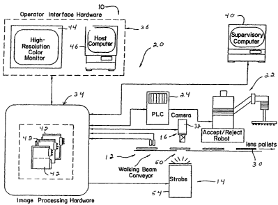
Figure 1 illustrates inspection system 10 for inspecting contact lenses.
System 10 generally comprising transport subsystem 12, illumination
subsystem 14, imaging subsystem 16 and processing subsystem 20. Figure
11
CA 02444517 2003-10-21
WO 03/073061 PCT/US03/05356
1 also shows reject mechanism 22, reject controller 24, and a plurality of
lens
carriers or pallets 30, each of which holds one or more lens packages.
Preferably, imaging subsystem 16 includes camera 32; and processing
subsystem 20 includes image processor means 34, operator interface means
36, and supervisory computer 40; and, more specifically, processor means 34
includes a plurality of processor and memory boards 42, and interface means
36 includes monitor 44 and host computer 46.
Generally, transport subsystem 12 is provided to move a multitude of
ophthalmic lenses along a predetermined path and into a lens inspection
position, referenced at 50 in Figure 1. Illumination subsystem 14 is provided
to generate a light beam which includes light comprising one or more bands
that are at least partially absorbed and one or more different bands that are
at
least partially transmitted and to direct that beam through the lenses moving
through the lens inspection position. Imaging subsystem 16 generates a set
of signals representing the light beam, or portions thereof, transmitted
through
each inspected lens, and then transmits those signals to processing
subsystem 20.
Processing subsystem 20 receives those signals from imaging
subsystem 16 and processes those signals according to a predetermined
program. Using this program, processing subsystem 20 generates a signal
indicating whether each inspected lens is suitable for consumer use. If a lens
is found to be unacceptable, a signal is transmitted to controller 24, which
then operates mechanism 22 to remove the unacceptable lens from the
stream of acceptable lenses. Specific devices or elements that may be used
in system 10 are disclosed and described in detail in the above-mentioned
U.S. Patent 5,500,732 and U.S. Patent Application Serial No. 09/751,875,
both of which are herein incorporated by reference in their entireties.
Figure 2 illustrates in greater detail portions of the preferred lighting
and imaging subsystems. In use, a trigger sensor (not shown) detects a
carrier pack 30 moving along pack conveyor 52 and sends an electrical signal
to the lighting subsystem, which in turn fires xenon strobe 54 (light source).
Light produced by the strobe passes through diffusing glass 56 and migrates
12
CA 02444517 2003-10-21
WO 03/073061 PCT/US03/05356
through light extension tube 60, where it encounters a combination of filters
62 and 64 in a filter holder 66. Newly filtered light continues on its course
through the primary package 70, where the light encounters the contact lens
in de-ionized water 72. Light emerging from the contact lens is received by
the multi-element quartz lens 74 and optically processed before it impinges
the camera CCD array 76. The resultant image data are then processed by
the processing subsystem. Figure 2 also shows a camera lens f-stop
adjustment ring 80, a lens extension tube 82, and a lens focus ring 84.
The filters, 62 and 64 remove the wavelengths of light that are not
within the first wavelength band or the second wavelength band. Preferably
one of the filters is an IR filter with a peak transmission at 540 nm 300 FWHM
(Full width at half max., or the width of the transmitting band of an optical
filter
measured at 50% of the peak transmission.) The second filter is preferably a
uv filter, either a UV transmitting black glass filter that filters light at
350 nm 53
FWHM (UG1 filter) or a black glass filter that filters light at 324 nm 112
FWHM
(UG11 ). The filters are described and shown in the preferred embodiments
as being located between the light source and the device to be inspected;
however, the filters may alternatively be located between the device to be
inspected and the camera.
With reference to Figure 1, in this operation of system 10, host
computer 46, which preferably includes a keyboard and a video terminal, is
connected to processor means 34 to display visually data or messages being
input into the processor. Monitor 44 is also connected to processor means 34
and is provided to produce video images from the data values stored in the
processor means, and monitor 44 may also be used to display inspection
results and totals.
As mentioned above, processing subsystem 20 processes the data
received from the pixel array 76 to determine whether each lens 70 is
acceptable. Generally, this is done by searching the image of each lens for
the presence of any defect, or more precisely, for the image of any defect. If
a defect is found, the lens is then rejected.
13
CA 02444517 2003-10-21
WO 03/073061 PCT/US03/05356
One type of defect is a hole in a lens, and prior art inspection
procedures typically search for such holes. A key disadvantage of the prior
art technology, however, is its inability to discern accurately between
bubbles
in solution 72 and holes in a contact lens 70. This inability is due to the
fact
that these bubbles 42 and holes 43 have similar characteristics when imaged.
This deficiency is a leading cause of falsely rejected product.
The illumination subsystem 14 is designed and operated to form an
image on pixel array 76 in which bubbles and holes have discernable
differences, and processing subsystem 20 is provided with a routine that can
identify those differences and thereby distinguish between holes in the lenses
and bubbles in the solution. More specifically, the illumination subsystem
provides a plural-wavelength imaging method for the lens, whereas the lens
has varied absorption levels, comprising at least one illumination source
comprising wavelengths that are at least partially absorbed and wavelengths
that are at least partially transmitted by the lens to produce a partially
translucent image.
In addition to the spectral qualities of the contact lens, this technique
may add quantities of ultraviolet inhibitors to the remaining contact lens
components to adjust the degree of absorbance of the wavelength band to
achieve the desired translucent effect. With reference to Figure 3, the effect
is achieved by passing bands of filtered ultraviolet and visible light in the
appropriate ratio and intensities through the lens, and the net result is
bands
86 and 88. The spectral bands are selected in such a manner that a portion
of the ultraviolet light is absorbed by the lens and a portion of the visible
light
is allowed to pass through the lens. The uv portion of the light that reaches
the camera and is part of the light that forms the image on the CCD array
preferably comprises 340-365nm. (This uv portion of the light is measured
after passing through the filters and the contact lens.) The visible portion
of
the light that reaches the camera and is part of the light that forms the
image
CCD array preferably comprises 385-405 nm. (This visible portion of the light
is measured after passing through the filters and the lens.) The ratio of
absorptive (ultraviolet light component) to non-absorptive (visible light
14
CA 02444517 2003-10-21
WO 03/073061 PCT/US03/05356
component) is preferably between about 1:1 to 1.5:1 and more preferably
1.5:1.
Also, the system is adjusted so that the average intensity of the light
comprising the said first wavelength band and said second wavelength band
incident on the photo-sensitive pixel array is in the mid-range of the
sensitivity
of the array. For example if the corresponding gray scale reading range of the
photo-sensitive pixel array is for example 0 to 255, the average intensity of
the
light incident on the photo-sensitive pixel array is adjusted to the middle of
this
range preferably about 140. In Figure 3, line 92 (" ") represents the
camera/filtertransmittance, line 90 ("____") represents the lens absorption
data without filters present, and line 94 ("_ _ _ _'), which includes bands 86
and
88, represents the net transmittance spectra at the camera after passing
through the lens and filters. Figure 4 illustrates a contact lens image 96
formed on the pixel array using this multi-spectral imaging technology. The
contact lens image is a partially translucent image i.e. a gray image, 97.
This
image clearly distinguishes between bubble, 42, and hole 43. By contrast, a
bright field inspection system creates a bright image of the contact lens in
which the edge and defects are dark pixels, and a dark field inspection system
creates a dark image of the contact lens in which the edge and defects are
bright pixels.
Figure 5 shows a flow chart for a routine or procedure 100 that is
performed by the processing system using a computer program to analyze
pixel information. The procedure, when used with a lens image formed in the
above-described manner, is able effectively to distinguish between holes in
the lenses and bubbles in the liquid in which the lenses are submerged.
Generally, this procedure employs three key elements to discriminate bubbles
from holes: symmetry, wall thickness, and intensity and intensity ratios. All
the discrimination features can be used in any inspection system, e.g. bright
field and dark field inspection systems as disclosed in US Patents 6,154,274;
5,995,213; 5,943,436; 5,828,446; 5,814,134; 5,812,254; 5,805,276;
5,748,300; 5,745,230; 5,717,781; 5,675,962; 5,649,410; 5,640,464;
5,568,715; and 5,500,732, which are hereby incorporated by reference in their
CA 02444517 2003-10-21
WO 03/073061 PCT/US03/05356
entirety. However, the third discrimination feature using intensity and
intensity
ratios is particularly well-suited to the system described herein.
Bubbles have an aspect ratio, which is a measure of symmetry, close
to 1.0, where the aspect ratio is defined as the width divided by the height
of
the bubble. Bubbles also have symmetrical structures within as well. The
inertial centroid (center of intensity similar to center of mass) of a bubble
is
almost always within, one or two pixels of its geometric centroid. The
inertial
centroid is defined by the following equations:
Column: Xi = (pixel intensity) * (column position) / (Total Intensity Count)
Row: Yi = (pixel intensity) * (row position) / (Total Intensity Count)
The geometric centroid is its center and is defined by the following
equations:
Column: Xg = (column start) + (Width of the bubble)/2.0
Row: Yg = (row start) + (Height of the bubble)/2.0
Also, bubbles have a minimum wall thickness for their size. This wall
thickness is the dark ring that comprises the edge of the bubble. Holes often
have very thin edges, but the thickness of a hole's edge can vary with the
lens
prescription, location of the hole in the lens, and the depth of the hole. In
the
preferred routine 100, discussed in detail below, the bubble or hole wall
thickness is determined for eight search vectors, separated by 45 degrees,
processing from the outside to the center and comparing the pixels to
thresholds developed from the local background. For each vector, the dark
pixels and bright pixels are counted, based upon their comparison to the
thresholds. The dark pixels represent the thickness of the wall of the bubble
or hole and the bright pixel count is used to determine the amount of loss of
material, if any.
The above-described plural-spectral imaging technique provides an
additional discrimination feature: the intensities of a bubble and a hole with
respect to their respective local backgrounds. An important feature in the
16
CA 02444517 2003-10-21
WO 03/073061 PCT/US03/05356
preferred embodiment of this imaging techniques is that the lens absorbs over
99% of the UV light but passes almost all of the visible light. Because of
this,
the contact lens appears as a gray object (lower gray scale values) and any
significant loss of material in the lens will show up in the captured image as
white (higher gray scale values). Using this, holes can be easily detected in
the images by comparing their gray scale values to that of neighboring pixels.
One limitation in this discriminate is the discovery of bubbles which act as
tiny
lenses and refract the visible light, causing the bubbles to appear as holes.
They appear to be holes in the lens since they have brighter centers than its
neighboring pixels. In view of this, preferably, the bright pixel threshold is
linearly adjusted so that the dark to bright ratio threshold is relaxed to
allow
bright bubbles closer to the edge of the lens but to fail bright bubbles
closer to
the center of the lens.
With specific reference to Figure 5, preferably, before procedure 100 is
begun, the image data are processed to identify potential holes and bubbles,
which are generically referred to as blobs. Any suitable procedure may be
used to do this, for example, see US Patents 6,154,274; 5,995,213;
5,943,436; 5,828,446; 5,814,134; 5,812,254; 5,805,276; 5,748,300;
5,745,230; 5,717,781; 5,675,962; 5,649,410; 5,640,464; 5,568,715; and
5,500,732. All these patents are incorporated herein by reference in their
entirety. Typically a pixel-by-pixel analysis is performed which compares the
intensities of adjacent pixels to first locate the edge of the lens and then
to
determine if the lens has any defects within the lens. The pixels within the
lens are compared to a threshold value and if the pixel intensity is less than
the threshold value, then that pixel may be a hole or a defect. Adjacent
pixels
having an intensity lower than the threshold value are grouped together and
will be referred to as a blob. A rectangular region is defined around each
blob
incorporating all the pixels of the blob having intensity values less than the
threshold value. At step 102 of procedure 100, the total number of blobs is
compared to a threshold value; and if that number exceeds this threshold
value, the lens is rejected and the routine ends. This is done on the premise
that, if so many blobs are present, it is very likely that at least one of the
blobs
17
CA 02444517 2003-10-21
WO 03/073061 PCT/US03/05356
is a hole, or even if all the blobs are bubbles, these bubbles may have
obscured or masked a hole in the lens. Under these circumstances, it may
simply be more economical to reject the lens than to analyze all the blobs.
For example, the threshold value may be 50 as shown in Figure 5.
If the total number of blobs is less than the threshold value, the routine
proceeds to analyze the blobs one at a time. Specifically, at step 104, the
size of one of the blobs is compared to a minimum value that represents the
smallest size a hole would likely have. If the blob is not greater than this
minimum hole size, the blob is considered not to be a hole, and the routine
proceeds to analyze the next blob. For the preferred system, a blob smaller
than 3 pixels, 47 microns is considered not to be a hole.
In contrast, if the size of the blob is such that it could be a hole, then
the routine goes to step 106 and the aspect ratio of the blob is calculated.
As
mentioned above, this aspect ratio is simply the width of the blob divided by
its height. At step 110, this aspect ratio is compared to a range, and if the
aspect ratio is outside the specified range, than the blob is identified as a
hole, and the routine proceeds to analyze the next blob. If, however, the
aspect ratio is within the range, the routine moves on to step 112. The aspect
ratio is usually set to be within the range of 0.8 to 1.2.
It may be noted that the range to which the aspect ratio is compared at
step 110 does not have to be a permanent, fixed range, but may vary from
blob to blob depending on the size of the blob. For example, one value may
be used for this comparison if the blob is larger than a given size, while a
second value may be used if the blob is smaller than a given size. Also, if
the
blob is smaller than a given size, a comparison value may be determined as a
function of the blob size. Large bubbles usually have thicker edges so the
program may provide a more narrow aspect ratio range centered close to 1 to
optimize differentiation of large bubbles by relying more on the analysis of
their edge thicknesses.
At steps 112 and 114, several values are calculated. In particular, at
step 112, two threshold values are calculated. A first of these, referred to
as
the hole threshold, represents a background relative intensity for comparison
18
CA 02444517 2003-10-21
WO 03/073061 PCT/US03/05356
for pixels inside the blob; and the second value, referred to as the ring
threshold, represents a background relative intensity for comparison for
pixels
on the edge, or ring, of the blob.
For each blob processed, an estimation of the local background is
performed to support a better determination of thresholds used for evaluating
the blob size, shape, and characteristics. The thresholds determined from the
local background include a hole threshold, a ring threshold, and a debris
threshold. The hole threshold is used to identify partial holes where the blob
interior is not at saturated levels, but is brighter than the local background
gray levels. The blob wall threshold is used to evaluate the potential bubble
wall thickness since a bubble image appears as a dark circular ring shape
much like a donut. The bubble interior is usually similar in intensity to its
local
background levels, but bubble blobs usually exhibit a dark ring, which is
significantly darker than the local background levels. A threshold is also
determined separately for debris, which typically are darker than the bubble
wall intensities. The use of the local background to set these thresholds
means that the processing will be more adaptive and each blob processed will
be better characterized.
Any suitable procedure may be used to determine an appropriate local
background value for each blob. Preferably, this value may be based on the
intensity values of the pixels in a defined area neighboring the blob and
inside
the rectangle that defines the analysis area for the blob. Using this just-
determined background value, BgMean, the hole ring, and debris threshold
values may be calculated by the equations:
holeThrs = BgMean + (C smHTFactor * BgSigma)
ringThrs = BgMean + (C smDTFactor * BgSigma)
Where BgMean is the mean intensity value of the pixels in a given area,
BgSigma is the standard deviation of these pixel intensity values from the
mean, and C smHTFactor and C smDTFactor are parameters. These
parameters are empirically derived by an iterative process for a system using
19
CA 02444517 2003-10-21
WO 03/073061 PCT/US03/05356
images of contact lenses that are known to have holes and bubbles in the
images.
At step 114, a blob gradient value (described below as a first derivative
in two-dimensions)for each pixel of the blob is determined. An important part
of the initial blob analysis, preceding step 102, i.e. preceding the bubble
processing software shown in the flow diagram in Fig. 5, is the determination
of the blob edges by calculating its first derivative in two-dimensionals or
gradients. These gradients are used to track the exterior and interior edges
to
form a blob for later processing. However, these gradient values are replaced
in the initial blob analysis with pixel color coding which is used to stitch
neighboring pixels together into one contiguous blob. As a part of the bubble
identification process, the blob edge gradients are reevaluated at step 114.
The blob gradient reevaluation is comprised of calculating the first
derivatives
in two-dimensions for an increased area size for each blob (2 additional
pixels
on each side of the initial blob rectangular region) in an attempt to enhance
weak edges that may have been overlooked by the initial blob analysis that
was done prior to step 102 when the blobs were located. While the blob
gradient is recalculated, the gradient mean and standard deviation is
calculated. The gradient threshold is determined to be the gradient mean
minus one gradient standard deviation. The gradient threshold is utilized in
later processing to determine the blob size, aspect ratio, symmetry, and blob
wall (ring) thickness, which are used to classify the blob as a bubble or a
defect. In the initial blob analysis, performed before step 102 in the bubble
identification software, is a static gradient threshold is used in the blob
analysis. By calculating a local gradient threshold for each blob in the
bubble
processing software, a better assessment of the blob characteristics can be
performed.
After steps 112 and 114, the routine determines, at step 116, whether
the blob is small or large. This is done by comparing the size of the blob to
a
predetermined parameter. If the size is less than this constant, the blob is
considered small, and the routine proceeds to step 120; and if the blob size
is
CA 02444517 2003-10-21
WO 03/073061 PCT/US03/05356
greater than this constant, the blob is considered large and the routine move
to step 122.
Small blobs, which are smaller than the value specified by the
parameter C_bubMinBlob, for example blobs having a pixel area greater than
15, and which have an aspect ratio within the specified range of the
parameter C smBubRat, are evaluated to determine if they have bright pixels
characteristic of small holes. Also, the ratio of dark pixels to all pixels
(determined by comparison of pixel intensities to the hole and ring thresholds
calculated from the local background (for each blob)) is compared to the
parameter C_minDPPer. If the dark pixels to total pixels within the blob is
greater than C_minDPPer, then the blob is a bubble or a small partial hole.
C_minDPPer is determined empirically for a given system and lens. For the
present system it has a value of 52.
At step 120, the ratio of dark pixels to all pixels is calculated, and then,
at step 124, this ratio is used to determine whether the blob is a hole or a
bubble. More specifically, at step 124, two criteria must be met in order for
the blob to be identified as a bubble. The first criterion is that the ratio
of dark
to total pixels must satisfy a given condition. For example, this condition
may
be that the ratio of dark to total pixels be greater than a defined value. It
should be noted that this defined value may be a function of other factors
such as the size of the blob. The second criterion applied at step 124 is
whether the total number of bright pixels is less than a given number such as
two. If both of the criteria applied at step 124 are met, the blob is
identified as
a bubble, and otherwise the blob is determined to be a hole.
At step 120, any suitable test or tests may be used to identify pixels as
dark or bright. For instance, those pixels whose intensity values are less
than
a first, given value may be considered as dark, while the pixels whose
intensity values are greater than a second value may be considered as bright.
For the present system, it is preferred that a dark pixel is a pixel having an
intensity value less than the ring threshold, ringThr, and a bright pixel is a
pixel having an intensity value greater than the hole threshold, holeThr.
21
CA 02444517 2003-10-21
WO 03/073061 PCT/US03/05356
If, at step 116, the blob is determined to be a large blob, the routine
proceeds from step 116 to step 122, where the size of the blob is compared to
a given value (which is a parameter with a default value of 11000 pixels
square), which represents the maximum size of a bubble. If the blob is not
smaller than this value, the blob is identified as a hole. However, if the
blob is
smaller than this size, the routine moves to step 126, where the thickness of
the ring, or outside edge, of the blob is determined.
Larger blobs have their wall thickness evaluated to determine if they
exhibit the characteristic trait of bubbles in that they resemble a donut. The
blob wall thickness is determined, at step 126, along each of eight search
vectors, separated by forty-five degrees, processing from outside the blob to
the center, and comparing the intensity values for pixels on the vector to
hole
and ring thresholds calculated from the local background for each hole. Along
each vector, the dark pixels and bright pixels are counted, based on their
comparison to the ring or hole thresholds. The dark pixels represent the
thickness of the wall (edge or ring) of the blob, and the bright pixel count
may
be used to determine the amount of loss of material, if any.
At step 130, the number of vectors that extend through a wall thickness
greater than a given number of pixels above a minimum thickness, e.g.
greater than two pixels, is compared to a given value, C-bubNEdge. If the
blob fails this test , then the blob is classified as a hole (defect). If the
blob has
an acceptable number of test vectors, then it is further processed to
determine
if it is a bubble.
If a blob passes the ring vector test in step 130, then its pixels are
compared to additional thresholds determined from the local background and
counted. Also the geometric mean and pixel weighted mean are determined.
The additional threshold values are:
darkThr = BgMean - (darkfac * BgSigma)
brightThr = BgMean + (holefac * BgSigma)
verybrightThr = holeThr
As described above the parameters darkfac and holefac are determined
empirically as described earlier.
22
CA 02444517 2003-10-21
WO 03/073061 PCT/US03/05356
At step 132, counts are made of the number of pixels inside the blob
that are dark, bright, and very bright. Specifically, to do this, the gray
level
values for the pixels are compared to the three threshold values just defined,
representing dark, bright and very bright values. If a pixel's gray level
value is
less than the dark threshold value (darkThr), the pixel is considered to be
dark. If a pixel's gray level value is greater than the bright threshold value
(brightThr), the pixel is considered to be bright; and if a pixel's gray level
is
greater than the very bright threshold value (verybrightThr)" the pixel is
considered to be very bright . With this procedure, it may be noted, a pixel
that is very bright is also counted as a bright pixel.
At step 134, the routine checks to determine if the blob has any bright
pixels. If not, the blob is considered to be a bubble; while if the blob has
any
bright pixels, the routine proceeds to step 136 to test if the blob is a
bubble
that has a bright center because the bubble is acting as a lens. At this step,
an assessment is made, based upon the number of dark and bright pixels and
a comparison of the geometric center and the inertial centroid that was
described earlier and may be referred to as a pixel weighted mean, to
determine whether the blob is a bubble, hole, debris, or some other type of
defect. When bubbles exhibit bright pixels in their center region, their
inertial
centroid is typically very close to their geometric centers, whereas holes
often
will appear to have skewed inertial centroids when compared to their
geometric centers. Debris is usually also nonsymmetric and will also fail this
test.
At step 140, the distance between the inertial centroid and geometrical
center is compared to a defined value, which may be a constant, or may be
determined according to a defined function. If this distance is not less than
the defined value, the blob is considered to be asymmetrical and is thus
considered to be a hole. However, if the distance between the inertial and
geometric centroids is less than the defined value, the blob is considered to
be symmetrical. The blob may be a bubble, and the routine moves on to step
142.
23
CA 02444517 2003-10-21
WO 03/073061 PCT/US03/05356
At this step 142, the routine checks to see if the ratio of dark pixels to
bright pixels indicates whether the blob is a bubble. To do this, the routine
compares that ratio to a defined value, which may be a parameter or which
may be calculated according to a defined function. If the ratio of dark to
bright
pixels is less than the defined value, the blob is considered to be a bubble,
but
if this ratio is not less than the defined value, the blob is considered to be
a
hole. The defined value is preferably approximately 5.
With the preferred embodiment of routine 100 shown in Figure 5, all the
blobs may be analyzed, even though the presence of one hole may be
sufficient to reject the lens. It is preferred that all the blobs be analyzed
as
this may provide useful information about the procedure used to make the
lens.
Figures 6 and 7 illustrate an inspection system 200 embodying an
alternate system and method of this invention. As will be appreciated, Figures
6 and 7 are similar to Figures 1 and 2, respectively, and like reference
numbers in the Figures identify identical or counterpart subsystems or
elements. Thus, system 200 of Figures 6 and 7 comprises transport
subsystem 12, illumination subsystem 14, imaging subsystem 16 and
processing subsystem 20. With particular reference to Figure 7, in system
200, the illumination subsystem includes xenon strobe 54, and the imaging
subsystem includes camera 32, which includes CCD array 76. The difference
between the system shown in Fig.1 and Fig. 6 is that the contact lens is
shown as being inspected in a mold half or front curve mold 206, instead of
the final package as described for the system shown in Figures 1 and 2. This
system using light that is partially transmitted and partially absorbed is
particularly useful, because it can be used to inspect thick and thin contact
lenses, as compared to other systems, particularly an inspection system using
uv light alone, that can be used to inspect thin lenses, but cannot create an
image through a thick lens.
As will be understood by those skilled in the art, system 200 is
designed to inspect a molded contact lens, which was molded between two
mold sections, shortly after one of the mold sections is removed. The lens is
24
CA 02444517 2003-10-21
WO 03/073061 PCT/US03/05356
left in the remaining mold section 206, which then carries the lens through
the
inspection system. In the vast majority of times, the two mold sections are
pulled apart without affecting the lens. However, on some occasions as the
mold sections are pulled apart, a lens may be slightly pulled away from the
remaining mold section. This is not a defect in the lens. However, typical
prior art automated lens inspection systems are not able to distinguish
effectively between a lens that has pulled away from a mold section and a
lens that holes or tears, which are defects.
Therefore the invention includes a method of inspecting an optical
device comprising
(a) illuminating the center zone of said optical device with light having a
first bandwidth;
(b) illuminating the edge of said optical device with light having a second
bandwidth;
(c) transmitting the light of step (a) and step (b) through said optical
device
and capturing said light on a photo-sensitive pixel array;
(d) reading the pixels generated from step (c) to inspect said optical
device.
As used herein, the terms optical device and photo-sensitive pixel array have
their aforementioned meanings and preferred ranges. The term "center zone"
refers to area of said optical device that concentrically extends from the
geometric center of the optical device of said optical device to a radius of
no
greater than about 1 millimeter from the edge of said optical device. As used
herein, the term "edge" refers to the area of said optical device that
concentrically extends from the perimeter of said optical device and ends at
said center zone. For example if said optical device is a contact lens having
a
diameter of 12.6 millimeters the center zone is the area, extending from said
the geometric center 5.3 millimeters when measured along the radius. The
edge of this contact lens is 6.3 millimeters measured along this radius.
As used herein the phrase " light having a first bandwidth" refers to light
having a wavelength that illuminates defects such as hole, bubbles, tears, and
debris in optical devices. Preferably said light having a first bandwidth is
in
CA 02444517 2003-10-21
WO 03/073061 PCT/US03/05356
the visible range, (about 370 nm to about 410 nm), however, said light having
a first bandwidth may comprise light in the visible range and the ultraviolet
range. For example light having a first bandwidth may have a first wavelength
band and a second wavelength band as said terms are defined herein. The
phrase, "light having a second bandwidth" refers to light having a wavelength
that does not produce any image feature resulting form a slight separation of
the lens edge from the mold carrier. It is preferred that said light having a
second bandwidth be in the ultraviolet region of the spectrum (about 330nm to
about 367 nm).
Still further the invention includes a method of inspecting an optical
device comprising
(a) illuminating the center zone of said optical device with light having a
first bandwidth;
(b) illuminating the edge of said optical device with light having a second
bandwidth;
(c) transmitting the light of step (a) and step (b) through said optical
device
and capturing said light on a photo-sensitive pixel array;
(d) producing an image of said optical device.
As used herein, the terms optical device, photo-sensitive pixel array, image,
center zone, edge, light having a first bandwidth and light having a second
bandwidth have their aforementioned meanings and preferred ranges.
Yet still further the invention includes an apparatus for inspecting an
optical device comprising
(a) a means for illuminating the center zone of said optical device with
light having a first bandwidth;
(b) a means for illuminating the edge of said optical device with light
having a second bandwidth;
(c) a means for transmitting the light of step (a) and step (b) through said
optical device and capturing said light on a photo-sensitive pixel array;
(d) a means for reading the pixels generated from step (c) to inspect said
optical device.
26
CA 02444517 2003-10-21
WO 03/073061 PCT/US03/05356
As used herein, the terms optical device, photo-sensitive pixel array, image,
center zone, edge, light having a first bandwidth and light having a second
bandwidth have their aforementioned meanings and preferred ranges.
As used herein said means for illuminating said center zone include but
what are not limited to transmitting light from a light source through a first
filter
element, wherein said filter transmits light that shows holes and tears in
said
optical device. Preferably said first filter element transmits light in the
visible
range of the spectrum, more preferably about 370 nm to about 410 nm. As
used herein means for illuminating said edge include but are not limited to
transmitting light from a light source through a second filter element,
wherein
said filter does not produce an image feature resulting from a slight
separation
of the lens edge from the mold carrier. Preferably said second filter element
transmits light in the ultraviolet region having a wavelength of about 330 nm
to
about 367 nm. This invention is illustrated in more detail in reference to the
following figures and description.
In an alternative preferred embodiment of the system shown in Figures
6 and 7, system 200 can be modified to exchange the filter device 202 located
between the light source 54 and the lens 204 to with another filter device be
220 shown in Figure 8. Alternatively, the filter device, 220, could be located
between the lens 204 and the camera.
With the filter device 220, system 200 is designed to avoid rejecting
lenses simply because they are delaminated. Generally, this is done by
utilizing the fact that most holes and tears in lenses occur in the central
regions of the lenses, while the effect of a lens that has pulled away from
the
mold carrier 206 is apparent primarily in the peripheral area of the lens.
More
particularly, the illumination subsystem of system 200 is designed and
operated to form an image on pixel array 76 that effectively shows holes or
tears in a lens without also showing any effects resulting from slight
separation of the lens from the mold carrier.
Preferably this is done by illuminating the central region of a contact
lens 206 with light in at least one bandwidth that shows holes or tears in the
lens, and illuminating the outer regions of the lens with light in a second
27
CA 02444517 2003-10-21
WO 03/073061 PCT/US03/05356
bandwidth that does not produce any image feature resulting from a slight
separation of the lens edge from the mold carrier. This, in turn, is
accomplished by positioning filter device 220 in the path of the illumination
light beam, between light source 54 and lens 204.
Filter device 220 comprises a holder or a body member, and a first and
a second filter elements, which are securely held in the body member. With
particular reference to Figure 8, a first filter element 212 has a circular
shape,
and a second filter element 214 has a larger circular shape and is positioned
so that 214 is concentric with said first filter element 212 so that said
second
filter element, 214 overlaps with said first filter element 212, and also has
an
annular shape that extends beyond the circumference of filter element 212. .
Alternatively, a circular first filter element and an annular second filter
element
could be used to achieve the same effect.
Filter device 220 is positioned in system 200 so that light that passes
through the central portion of the lens 204 passes through said first filter
element 212, and light that passes through the outer peripheral portion of the
lens 204 has passed through said second filter element 214. Moreover,
preferably, none of the light that passes through said first filter element
212
passes through the outer lens region, and, similarly, none of the light that
passes through said second filter element 214 passes through the central lens
region.
Filter elements 212 and 214 may transmit any suitable bandwidths.
For instance, said second filter element 214 transmits light in the ultra
violet
region of the spectrum, preferably at approximately 340nm or 357nm (+/-
10FWHM) to provide ultraviolet style illumination for the lens periphery. Said
first filter element 212 transmits light mostly in the visible region, but can
transmit light in the first wavelength band, 86, and the second wavelength
band, 88 as shown in Figure 3. By narrowing the bandwidth of light that is
able to be transmitted to the outer portions of the lens and ultimately to the
CCD array, the image of the outer portions of the lens is a darker image that
masks artifacts of delamination.
28
CA 02444517 2003-10-21
WO 03/073061 PCT/US03/05356
Figure 9 illustrates a lens image formed on pixel array 76 of system
200. Any suitable image analysis algorithm may be used to analyze the pixel
data to determine if the lens is acceptable. A significant advantage of this
aspect of the invention is that existing image analysis algorithms can be used
to determine whether the lens has holes or tears. This is due to the fact that
the use of uv light only on the edge of the lens masks the artifacts of the
demold process that appear as delamination. spectral masking technique
employed in system 200 eliminates, or at least substantially reduces, the
likelihood that a feature appears on pixel array 76 due to lens separation
from
the mold carrier. Thus, algorithms can accurately identify lenses that have
holes or tears even if the algorithm is not able effectively to distinguish
between such lenses and a lens whose edge has separated from the mold
carrier.
As will be appreciated by those of ordinary skill in the art, system 10,
routine 100 and system 200 may be used to inspect a large variety of types
and sizes of optical lenses and other optical devices, and systems 10 and 200
are particularly well suited for inspecting contact lenses. Further, the
plural-
spectral imaging procedures disclosed herein can also be applied to other
objects using various combinations of the spectrum depending upon the
absorption/transmission characteristics of the object to be inspected and/or
packaged in the system. Other objects that can be inspected using this
invention include spectacle lenses, camera lenses, optical filters, thin
films,
and glass.
Additional aspects of the invention disclosed herein include but are not
limited to the following. A method of reading pixels generated from photo-
sensitive array to evaluate the whether an optical device comprises a hole, by
using the degree of symmetry, a wall thickness, and the gray scale values of
said optical device. A program storage device readable by machine, tangibly
embodying a program of instructions executable by the machine to perform
method steps for processing image data representing an optical device which
distinguishes defined characteristics of said optical device.
29
CA 02444517 2003-10-21
WO 03/073061 PCT/US03/05356
While it is apparent that the invention herein disclosed is well
calculated to fulfill the objects stated above, it will be appreciated that
numerous modifications and embodiments may be devised by those skilled in
the art, and it is intended that the appended claims cover all such
modifications and embodiments as fall within the true spirit and scope of the
present invention.