Note: Descriptions are shown in the official language in which they were submitted.
CA 02444687 2003-10-15
WO 02/084876 PCT/US02/09233
FLEXIBLE CAPACITIVE TOUCH SENSOR
TECHNICAL FIELD
This invention relates to touch sensors and, in particular, to capacitive
touch
sensors and to a method of manufacturing capacitive touch sensors.
BACKGROUND OF THE INVENTION
Touch sensors are widely used to provide a user-friendly interface to a
computer
system. The sensor usually is affixed over the computer system's monitor to
enable the
user to directly interact with the system through the monitor by means of
finger-touch or a
stylus.
Touch sensors fall into two broad categories, namely, digital touch sensors
and
analog touch sensors. The touch surface of a digital touch sensor is
segregated into a
plurality of discrete segments. Each of these segments produces a discrete
signal when
touched. Sensing resolution is limited, therefore, to identifying the
particular segment
contacted by a finger or stylus. The signal from an analog touch sensor, on
the other hand,
is not discrete. Sensing resolution is limited only by the overall sensitivity
of the sensor
and its controlling electronics.
Both analog and digital touch sensors employ a variety of techniques to
determine
the point at which a finger or stylus contacts the touch surface. These
techniques include
2 0 resistive sensing, capacitive sensing, acoustic sensing and optical
sensing. The vast
majority of touch sensors, however, use either resistive sensing or capacitive
sensing
techniques.
A resistive touch sensor employs a flexible membrane positioned over a
substrate.
The opposing surfaces of the membrane and substrate are coated with a
transparent
conductive film. Insulating dot spacers are interposed between the membrane
and the
substrate. When the flexible membrane is pressed by a user, the conductive
film of the
membrane contacts the conductive film of the substrate. This contact causes
current to
flow between the membrane and substrate. A controller identifies the point of
contact by
comparing the current flowing from various electrodes or busbars printed on
the
3 0 conductive surfaces.
A capacitive touch sensor employs no moving parts. In a capacitive touch
sensor,
a resistive coating is deposited directly upon a solid, insulating substrate.
This substrate
-1-
CA 02444687 2003-10-15
WO 02/084876 PCT/US02/09233
usually is made of glass. Electrodes positioned at the corners of the
substrate establish an
electrical field on the coating. A controller connected to these electrodes
monitors the
amount of current flowing through each of these electrodes. A user's finger,
or a
conductive stylus, touching, or coming within close proximity to, the
resistive coating
causes capacitive coupling between the finger or stylus and the coating. This
coupling
causes a small amount of current to flow through the coating and each of the
electrodes.
Capacitive coupling through the user's body and ground complete the current
path back to
the controller. The controller calculates the Cartesian coordinates, i.e., the
X and Y
coordinates, of the point of touching from the amount of current flowing
through each of
these electrodes.
Capacitive touch sensors also can function to detect the proximity of an
object to
the touch sensor. In this, case, physical contact with the touch sensor is not
required.
Capacitive coupling occurs between the object and the sensor through the space
separating
the object from the sensor.
Since resistive sensors require moving parts, they are more complex and often
more costly to manufacture than capacitive touch sensors. The optics of
resistive touch
sensors also are degraded by the sensor's multiplicity of separated layers
having different
refractive indices. Touch sensors located in bright environments require a low
reflection
touch screen to maintain display contrast. This problem is particularly acute
for resistive
2 0 touch sensors. Although an excessively bright display can overcome this
problem, such a
display requires additional electrical power and adds to the display's cost.
This solution,
therefore, is not desirable for a device operating on batteries.
Although analog capacitive touch sensors are less complex and provide better
optics, the solid, rigid substrate used on these devices diminish their
suitability for mobile
2 5 computerized systems, such as laptop computers, handheld computers,
cellular telephones
and the like. The weight of such sensors, and their capacity for breaking,
also are
important factors militating against their use in such systems. Mobile devices
also
experience far more mechanical flexing than stationary devices. A rigid,
brittle and heavy
component incorporated into such a device is incompatible with light, flexible
components
3 0 and could cause such flexible components to fail. Similar considerations
apply to displays
mounted in vehicles and large displays mounted on walls. Brittle, rigid
substrates also
-2-
CA 02444687 2003-10-15
WO 02/084876 PCT/US02/09233
increase the thickness of a display in products for which a low profile
provides a
commercial advantage.
Touch sensors based on glass substrates also require a specially fitted frame
for mounting the sensor over a monitor or display. Such frames further add to
the weight,
cost and complexity of the device. A flat, solid substrate also does not
conform well to
displays or monitors with uneven or curved surfaces, and bending rigid
substrates requires
expensive processing. Glass based touch sensors, moreover, must be
manufactured from
individual substrates of cut glass. Such manufacture is costly and time
consuming. All of
these deficiencies diminish the desirability of existing capacitive touch
sensors in some
applications.
SUMMARY OF THE INVENTION
The present invention overcomes many of the deficiencies of capacitive touch
sensors. The present invention provides an inexpensive, lightweight, flexible,
transparent
capacitive touch sensor and an efficient, low cost method of manufacturing
such a touch
sensor. Notwithstanding the low cost, lightweight and flexibility of a touch
sensor in
accordance with the present invention, the touch sensor has an unexpectedly
high
durability enabling it to perforn satisfactorily in numerous enviromnents and
with a wide
variety of devices. The present invention also provides a thin, transparent,
flexible layer
of protective material to protect the active touch area of a flexible,
transparent touch
2 0 sensor. This protective material substantially enhances the touch sensor's
performance and
durability.
In one aspect, the present invention provides a flexible, capacitive touch
sensor.
This touch sensor comprises a thin, flexible, transparent substrate having a
first side and a
second side. A first layer of resistive material is applied to the first side
of the substrate.
2 5 This first layer is thin, transparent, electrically continuous, flexible
and covers on the
substrate's first side a surface coincident with an active touch area. The
first layer is
adapted to receive an electrical potential across the first layer within the
active touch area
and to transmit an electrical signal indicative of the X and Y position of a
point at which
an object contacts the active touch area.
3 0 The flexible, capacitive touch sensor preferably includes a plurality of
thin, flexible
electrodes in electrical communication with the first layer. These electrodes
are positioned
along the periphery of the active touch area and are adapted to apply the
electrical
-3-
CA 02444687 2003-10-15
WO 02/084876 PCT/US02/09233
potential. The flexible, capacitive touch sensor also preferably includes a
plurality of thin,
flexible, electrical leads in electrical contact with the electrodes for
transmitting electrical
signals to and from the electrodes. A plurality of thin, flexible, conductive
areas also
preferably are included on the touch sensor. The conductive areas are in
electrical
communication with the first layer and are positioned along the periphery of
the active
touch area. The conductive areas form a pattern which is adapted to linearize,
within the
active touch area, the electrical potential throughout the first layer applied
by the
electrodes.
The flexible, capacitive touch sensor preferably also comprises a second layer
of
protective material. Depending upon the configuration of the touch sensor,
i.e., which side
of the substrate corresponds to the touch sensor's active touch surface, this
second layer is
on either the first layer or the substrate's second side. The second layer
also is thin,
transparent, flexible and covers within the active touch area substantially
the entire surface
of either the first layer or the substrate's second side. The mechanical
properties of the
protective material malce this second layer both flexible and durable. The
second layer
protects the active touch surface from wear and marring during use.
The touch sensor also may comprise a third layer of adhesive material. Again,
depending upon the touch sensor's configuration, this third layer may be on
either the first
layer or the substrate's second side. This third layer is thin, transparent
and flexible. This
2 0 third layer also preferably is pressure sensitive. The adhesive material
enables the touch
sensor to be attached to a supporting structure or display face. The third
layer preferably
covers within the active touch area substantially the entire surface of either
the first layer
or the substrate's second side. Covering substantially this entire surface
with this layer
provides smooth contact with the surface to which the touch sensor is affixed.
In the
2 5 alternative, the adhesive material may be applied in small amounts along
only the
periphery of the first layer or the second side.
The third layer of adhesive material preferably comprises a releasable sheet
covering the exposed' surface of this layer until the flexible touch sensor is
attached to a
display. This display may be a flexible display.
3 0 The electrodes, leads and conductive areas may be on the first layer of
resistive
material or on the substrate's first side. In the latter case, the first layer
of resistive
material covers the electrodes, leads and conductive areas. In another
embodiment, the
-4-
CA 02444687 2003-10-15
WO 02/084876 PCT/US02/09233
electrodes, leads and conductive areas are on the second layer of protective
material and
communicate with the first layer of resistive material through capacitive
coupling. This
capacitive coupling may be enhanced by imparting a low level of conductivity
to the
protective material. In other embodiments, the leads are deposited on either
the second
side of the substrate or on an insulating layer along the periphery of the
active touch area
covering the conductive areas.
The capacitive touch sensor preferably is connected to a controller for
providing
the electrical potential applied across the first layer within the active
touch area and for
receiving the electrical signal indicative of the X and Y position of a point
at which an
object, e.g., a person's finger or a conductive stylus, contacts the active
touch area. This
controller preferably provides a further electrical signal also indicative of
this X and Y
position. The controller preferably is connected to the electrical leads and
provides an
alternating voltage to the electrodes. The controller preferably monitors the
amount of
current flowing through each of these electrodes and, based upon these
amounts, provides
the further electrical signal.
The substrate preferably is a transparent sheet of polyethylene terephthalate
(PET)
having a thickness of between approximately 3 mils and 9 mils. The preferred
thickness is
approximately 7 mils. The first layer of resistive material preferably is a
layer of
transparent conductive oxide, e.g., indium tin oxide (ITO), indium oxide,
silicon indium
2 0 oxide, aluminum zinc oxide, indium zinc oxide, antimony tin oxide or tin
oxide, having a
resistance of between approximately 100 ohms per square and approximately
4,000 ohms
per square. This layer most preferably is ITO having a resistance of
approximately
1,000 ohms per square and a thiclcness of between approximately 200 angstroms
and
500 angstroms. In an alternative embodiment, the first layer comprises a first
coating of a
2 5 first resistive material in contact with the substrate's first side and a
second coating of a
second resistive material in contact with the first coating. The second
resistive material
preferably has a higher durability than the first resistive material. The
first resistive
material preferably is indium tin oxide, and the second resistive material
preferably is tin
oxide.
3 0 Conductive inlc may be used for depositing the electrodes, leads and
conductive
areas. This conductive ink preferably is silver epoxy conductive inlc. The
substrate may
include a tail extending from the substrate's periphery, and the electrical
leads may extend
-5-
CA 02444687 2003-10-15
WO 02/084876 PCT/US02/09233
over this tail. An electrical connector may be attached to the end of this
tail in electrical
contact with the leads.
The second layer of protective material preferably is fabricated from a resin
containing organosiloxane compounds combined with fluorine or methyl groups,
or
combinations of these compounds, to reduce the coefficient of friction of this
resin. The
resin preferably is an acrylate-based resin. The second layer also may contain
an
inorganic compound, such as silica, to increase this protective layer's
resistance to
abrasion. In an alternative embodiment, the second layer comprises a first
coating of a
first material in contact with the first layer of resistive material, and a
second coating of a
second material in contact with this first coating. For this embodiment, the
modulus
(hardness) of the first coating preferably is less than the modulus of the
second coating.
The first material for this embodiment may be a first polymer and the second
material may
be a second polymer, with the modulus of the first polymer being less than the
modulus of
the second polymer.
In yet another embodiment, the second layer of protective material contains a
substance to impart a low level of conductivity to this layer. This substance
may comprise
inorganic conductive particles or intrinsically conducting polymers. For this
embodiment,
the second layer of protective material preferably has a resistivity of
between
approximately 0.1 ohms-cm. and 1012 ohms-cm. As indicated above, imparting a
low
2 0 level of conductivity to the second layer increases the touch signal
transmitted between the
resistive layer and a finger or stylus.
The second layer of protective material also may comprise a roughened surface
to
diffuse light reflected from this surface. To provide this roughened surface,
the second
layer may contain transparent or translucent particles or may be mechanically
embossed.
2 5 The materials comprising these particles may also be chosen to reduce the
particles'
coefficient of friction and enhance the particles' resistance to abrasion.
In yet another embodiment, the flexible capacitive touch sensor comprises a
fourth layer
of conductive material. Depending upon the touch sensor's configuration, this
fourth layer
may be on either the substrate's second side or on an insulating layer
covering the first
3 0 layer of resistive material. This fourth layer shields the touch sensor
from interference
from excessive electromagnetic radiation, particularly excessive radiation
emitted from a
display to which the sensor is attached.
-6-
CA 02444687 2003-10-15
WO 02/084876 PCT/US02/09233
In another aspect, the present invention provides a method for manufacturing a
plurality of flexible, capacitive touch sensors. In accordance with this
method, a thin,
flexible, transparent substrate is provided. This substrate has a first side,
a second side and
is sufficiently large for division into a plurality of separate sections. Each
of these
sections corresponds to one of the capacitive touch sensors.
In accordance with this method, the substrate is passed by a plurality of
processing
stations, preferably by winding the substrate from a holding reel onto a
receiving reel. The
steps of the manufacturing process are performed at these processing stations
during this
process. The transmission of the substrate past these processing stations may
occur one or
more times. In accordance with this manufacturing process, a thin, flexible,
transparent,
electrically continuous first layer of resistive material is applied on the
first side of the
substrate. A plurality of thin, flexible electrodes, electrical leads and
conductive areas are
positioned on, or in communication with, the first layer of resistive
material. These leads,
electrodes and conductive areas are positioned along the peripheries of these
sections. A
thin, flexible second layer of protective material preferably is applied,
depending upon the
touch sensors' configuration, to either the first layer or the substrate's
second side. A
plurality of thin, elongated lines preferably are cut through the first layer,
or through the
first layer and the second layer, to substantially electrically isolate the
various electrical
leads from the conductive areas (except where these leads connect to the
electrodes). This
2 0 cutting preferably is done with a laser. The first layer, substrate and,
if present, the second
layer then are cut completely through, again preferably with a laser, along
the peripheries
of the various sections to provide the plurality of capacitive touch sensors.
This manufacturing process also may comprise applying, at one or more of the
processing stations, a thin, transparent, flexible layer of adhesive material
on either the
2 5 first layer or the substrate's second side (again, depending upon the
touch sensors'
configuration). In the alternative, this layer of adhesive material may be pre-
attached to
the substrate before passing the substrate through the manufacturing system.
The
substrate preferably is a sheet of polyethylene terephthalate (PET), and the
resistive
material preferably is indium tin oxide (ITO). The indium tin oxide preferably
is
3 0 deposited by vacuum deposition, e.g., sputtering. The electrodes, leads
and conductive
areas preferably comprise conductive inlc, most preferably silver epoxy
conductive inlc,
and this conductive ink preferably is deposited by screen printing or ink jet
printing. The
CA 02444687 2003-10-15
WO 02/084876 PCT/US02/09233
protective material preferably comprises acrylate-based resin modified to
increase surface
lubricity, and this resin preferably is deposited by spraying or Gravure
coating.
The manufacturing process also may comprise applying, at one or more of the
processing stations, a layer of conductive material to shield the sensor from
excessive
electromagnetic radiation. Depending upon the touch sensors' configuration,
this
conductive layer may be applied to either the substrate's second side or to an
insulating
layer covering the first layer. The process also may comprise affixing a
releasable sheet
over the exposed surface of the adhesive material. In the alternative, the
releasable sheet
may be pre-attached to the adhesive material.
BRIEF DESCRIPTION OF THE DRAWINGS
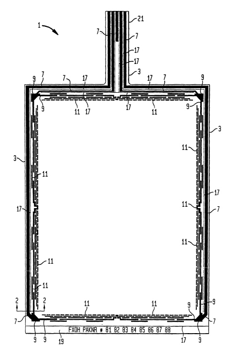
FIG. 1 is a plan view of a flexible, capacitive touch sensor in accordance
with the
present invention.
FIG. ~ is a schematic sectional view, taken along line 2-2 of FIG. 1, of the
flexible,
capacitive touch sensor shown in FIG. 1.
FIG. 3 is a schematic sectional view of an alternative embodiment of a
flexible,
capacitive touch sensor in accordance with the present invention.
FIG. 4 is a plan view of the flexible, capacitive touch sensor of FIG. 1
showing
only the electrodes, electrical leads and conductive areas.
2 0 FIG. 5 is a plan view of the flexible, capacitive touch sensor of FIG. 1
showing
only the laser cuts in the resistive layer.
FIG. 6 is a plan view of the flexible, capacitive touch sensor of FIG. 1
showing
only the substrate.
FIG. 7 is a plan view of an alternative embodiment of a flexible, capacitive
touch
2 5 sensor in accordance with the present invention.
FIG. 8 is a schematic diagram of a manufacturing system for manufacturing
flexible, capacitive touch sensors in accordance with the present invention.
FIG. 9 is a schematic diagram of a sheet of substrate material for use in
manufacturing flexible, capacitive touch sensors in accordance with the
manufacturing
3 0 system illustrated in FIG. 8.
_g_
CA 02444687 2003-10-15
WO 02/084876 PCT/US02/09233
DETAILED DESCRIPTION OF THE PREFERRED EMBODIMENTS
FIGURES l and 2 are a plan view and a schematic sectional view, respectively,
of
a flexible, capacitive touch sensor 1 in accordance with the present
invention. When
connected to an appropriate controller (not shown), touch sensor 1 detects the
point at
which an object, e.g., a user's finger or a conductive stylus, contacts, or
comes within close
proximity to, active touch area 2 of touch sensor 1. Touch sensor 1 provides a
signal
indicative of the caxtesian coordinates, i.e., the X and Y position, of this
point of contact.
Touch sensor 1 also may function to detect the proximity of an object to
active area 2.
Touch sensor 1 includes a thin, flexible, transparent, insulating substrate 3.
As
used in this specification and in the claims, a substance or material
described or recited as
being "transparent" includes substances or materials which axe only partially
transparent,
e.g., "translucent." Substrate 3, shown separately in FIG 6, is generally
rectangular in
shape and has an elongated tail 21 extending from one edge. The shape of
substrate 3 may
be other than rectangular, however, e.g., circular, square, triangular or
polygonal.
Substrate 3 preferably comprises a sheet of polyethylene terephthalate (PET).
In lieu of
PET, substrate 3 may be a flexible sheet of another suitable material, e.g.,
polycarbonate
polyester, polyvinyl chloride, polyether sulfone, polyimide polyether imide,
cellulose
triacetate and polyethelene naphthalate.
Substrate 3 preferably has a thickness of approximately 7 mils. The thiclcness
of
2 0 substrate 3 may range, however, from approximately 3 mils to approximately
15 mils.
Substrate 3 more preferably has a range of between approximately 3 mils and
approximately 9 mils. Substrate 3 should have a thickness, which is less,
however, than
that which may cause the materials applied to the substrate to be excessively
stressed
when the substrate is flexed. On the other hand, substrate 3 should not be so
thin that
2 5 handling and application to a display are excessively difficult.
As shown in FIG. 2, the topside of substrate 3 is coated with a thin,
transparent,
flexible layer 5 of resistive material. An appropriate material for resistive
layer 5 is a
transparent conductive oxide, preferably indium tin oxide (ITO). In the
alternative,
another transparent conductive oxide which can be applied to substrate 3 at a
relatively
3 0 low temperature may be employed, e.g., indium oxide, silicon indium oxide,
aluminum
zinc oxide, indium zinc oxide, antimony tin oxide or tin oxide. Resistive
layer 5 may be
applied to substrate 3 through vacuum deposition, e.g., sputtering. This layer
preferably
-9-
CA 02444687 2003-10-15
WO 02/084876 PCT/US02/09233
has a resistance of approximately 1,000 ohms per square. The resistance of
resistive layer
may range, however, from approximately 100 ohms per square to approximately
4,000
ohms per square.
Resistive layer 5 preferably comprises a continuous coating of material
covering
5 active area 2 of substrate 3. In the alternative, resistive layer 5 may
include some
discontinuities to improve the adhesion of materials applied to resistive
layer 5. For
example, resistive layer S may include a plurality of small apertures to
provide direct
contact between such materials and substrate 3. However, resistive layer 5
should be
electrically continuous within active area 2. In other words, a path should be
available
within active area 2 from every point on resistive layer 5 to every other
point on resistive
layer 5 without crossing a boundary of this layer.
The thickness of resistive layer 5 should be as small as possible to avoid
excessive
stress during flexing of touch sensor 1 and to improve optical transmissivity.
On the other
hand, the thicl~ness of resistive layer 5 should not be so small as to
jeopardize the
continuity of this layer or its material properties during manufacture. An
appropriate
thickness for resistive layer 5 is between approximately 200 angstroms and
approximately
500 angstroms.
In order to improve the ability of resistive layer 5 to withstand flexing,
scratching
and chemical changes during manufacture, this layer may consist of two
coatings, a first
2 0 coating of resistive material and a second more durable coating of
resistive material over
this first coating. The first coating preferably is ITO, and the second
coating preferably is
tin oxide (SnO2). Of course, other suitable materials may be used for this
purpose.
Referring again to FIGS. 1 and 2, touch sensor 1 also includes electrodes 9
deposited on the surface of resistive layer 5 near the corners of active area
2. These
2 5 electrodes are connected to electrical leads 7 and are adapted to apply an
electrical
potential across active area 2 within resistive layer 5. The pattern of
electrodes 9,
electrical leads 7 and conductive areas 11 (discussed below) deposited on
resistive layer 5
is shown separately in FIG 4.
Electrical leads 7 are deposited along the outer periphery of substrate 3 to
3 0 maximize the dimensions of active area 2. These electrical leads extend
from these
peripheral areas over tail 21 to an electrical connector (not shown) attached
to the end of .
tail 21. When touch sensor 1 is affixed to a display, this connector is
comlected to a
-10-
CA 02444687 2003-10-15
WO 02/084876 PCT/US02/09233
controller for transmitting an alternating voltage to electrodes 9. An
extension cable may
be used for this purpose. The controller also monitors the amount of current
flowing
through each of these electrodes. Based upon these amounts, this controller
provides a
signal indicating the X and Y position at which a person's finger or a
conductive stylus
contacts, or comes within close proximity to, active area 2. Such a controller
is described
in, e.g., U.S. Patent No. 4,353,552 (Pepper), the subject matter of which is
incorporated
herein by reference. Also, with an appropriate controller, touch sensor 1 also
can function
to detect the proximity of an object to active area 2. In such a case,
physical contact with
active area 2 is not required. Capacitive coupling occurs between the object
and active
area 2 through the space separating the object and active area 2.
Conductive areas 11 also are deposited on resistive layer 5 along the
peripheries of
substrate 3. Conductive areas 11 form a pattern, as is laiown in the art, for
linearizing
across active area 2 within resistive layer 5 the electrical potential
produced by
electrodes 9. A description of such a linearizing pattern of conductive areas
is provided in,
e.g., U.S. Patent No.4,371,746 (Pepper), the subject matter of which is
incorporated
herein by reference. This linearizing pattern causes the current flowing from
each of
electrodes 9 to correspond linearly with the distance between a given
electrode and the
point at which contact of active area 2 occurs. As indicated above, the
pattern of these
conductive areas is shown separately in FIG. 4.
2 0 Rather than deposit electrodes 9, electrical leads 7 and conductive areas
11 on
resistive layer 5, electrodes 9, electrical leads 7 and conductive areas 11
may be deposited
on the front side of substrate 3, and resistive layer 5 may be deposited over
electrical leads
7, electrodes 9 and conductive areas 11. Also, in order to maximize the
dimensions of
active area 2, electrical leads 7 may be deposited on the back side of
substrate 3, and these
2 5 leads may be connected to electrodes 9 by a conductive material, such as
conductive tape,
extending around the edges of substrate 3 or through apertures in substrate 3
coated with
conductive material.
In an alternative embodiment, in order to increase the dimensions of active
area 2,
a layer of thin, insulating material may be deposited along the periphery of
substrate 3
3 0 over resistive layer 5 and conductive areas 11. Electrical leads 7 then
may be deposited on
this insulating layer. This insulating material also may be deposited over
electrodes 9 and,
if so, apertures in the insulating layer, coated with conductive ink, may be
created to
-11-
CA 02444687 2003-10-15
WO 02/084876 PCT/US02/09233
provide an electrical connection between electrical leads 7 and electrodes 9.
The materials
and methods described in U.S. Provisional Patent Application No. 60/179,874,
filed on
February 2, 2000 and commonly assigned with the present application may be
employed
for this embodiment. The subject matter of U.S. Provisional Patent Application
No.
60/179,874 is incorporated herein by reference.
Electrodes 9, electrical leads 7 and conductive areas 11 consist of thin,
flexible
depositions of conductive inlc such as, for example, thermally cured silver
epoxy. This
conductive ink may be deposited on substrate 3 by screen-printing or ink jet
printing.
In order to enhance the appearance of touch sensor 1, and provide enhanced
protection to electrodes 9, electrical leads 7 and conductive areas 11, a
coating of
insulating ink (not shown) may be deposited over these electrodes, leads, and
conductive
areas. Information about touch sensor l, such as, e.g., a manufacturer's name,
manufacture's logo, product number, etc., may be printed using different
colors of such
ink. Also, identification area 19 (FIG. 1 ) on resistive layer 5 may be used
for printing
identifying indicia or other information using conductive or non-conductive
ink. If
conductive ink is used in this area, the area should be electrically isolated
from resistive
layer 5 by, e.g., a laser-cut line in resistive layer 5 as discussed below.
Referring again to FIG. 2, touch sensor 1 also includes protective layer 13.
This
layer preferably covers substantially the entire surface of resistive layer 5,
including
2 0 electrodes 9, electrical leads 7 and conductive areas 11. In the
alternative, protective layer
13 may cover only active area 2 or a portion of active area 2. Also, in a
further alternative
embodiment, electrodes 9, electrical leads 7 and conductive areas 11 may be
deposited on
protective layer 13. In this further alternative embodiment, electrical
communication
between these conductive areas and resistive layer 5 occurs through capacitive
coupling.
2 5 This capacitive coupling may be enhanced by imparting a low level of
conductivity to
protective layer 13, as discussed below.
Protective layer 13 preferably is a thin, flexible, transparent layer of
resin,
preferably thermally cured, acrylate based resin. In the alternative, this
resin may be cured
through exposure to ultra violet radiation, plasma radiation or electron beam
radiation.
3 0 The resin also may be chemically polymerized. The resin may be sprayed
over the
surface of resistive layer 5, electrodes 9, electrical leads 7 and conductive
areas 11. In the
alternative, this resin may be applied by pulling substrate 3 over a roller
coated with the
-12-
CA 02444687 2003-10-15
WO 02/084876 PCT/US02/09233
resin, as in the Gravure coating process, or deposited from a monomer source
in a vacuum.
Spraying is preferred, however, to avoid damage to the raised pattern of
electrodes 9,
electrical leads 7 and conductive areas 11 and to avoid discontinuities in
protective layer
13 that may be caused by pulling substrate 3 over such a roller. In another
alternative,
protective layer 13 may be applied by screen-printing. Although screen-
printing permits
depositing protective layer 13 selectively, this technique suffers from
manufacturing
inefficiencies when compared to spraying or the Gravure process.
Protective layer 13 protects resistive layer 5 from damage, which may result
from a
person's fingertips or fingernails, or coins, pens, jewelry and other
implements, contacting
active area 2. Protective layer 13 also serves to insulate the conductively
printed areas
from shorting by, for example, liquids spilled on this surface.
In order to enhance the feel and further enhance the durability of protective
layer
13, and also reduce flexing stresses between this layer and resistive layer 5,
compounds
may be combined with, or substituted for, the base resin to enhance the
lubricity of
protective layer 13, i.e., to reduce this layer's coefficient of friction.
These compounds
may include one or more compounds of siloxane, fluorine aald methyl groups.
For
example, coatable fluorothermoplastics such as those from Dyneon, or a
fluorinated
acrylate, such as 3M FluoradTM FX-189, may be used for this purpose. In lieu
of
combining such compounds with the base resin, such compounds may be applied as
an
2 0 overcoating over a harder underlying acrylate coat or over an underlying
coat of another
material providing enhanced adhesion to both resistive layer 5 and the
overlying coat.
Protective layer 13 also may be entirely formulated from organosiloxane
compounds, e.g.,
silicone, or compounds containing organosiloxanes, fluorocarbons or
combinations of
these compounds. In order to further enhance the ability of protective layer
13 to
2 5 withstand abrasion, inorganic compounds, such as silica, may be added to
the base resin
either alone or in combination with the above-identified compounds for
enhancing
lubricity.
In an alternative embodiment, protective layer 13 comprises two layers. The
first
layer is in contact with resistive layer 5 and is softer than the second
layer, which covers
3 0 the first layer aald is exposed to the environment. The modulus of the
first layer, therefore,
is less than the modulus of the second layer. This alternative embodiment
reduces stresses
-13-
CA 02444687 2003-10-15
WO 02/084876 PCT/US02/09233
between resistive layer 5 and protective layer 13 during flexing and,
therefore, diminishes
the extent to which stress fractures may occur in resistive layer 5 as a
result of flexing.
Such a bi-layered structure for protective layer 13 may be obtained by
fabricating
this layer from two polymers, each with a different degree of hardness. The
modulus of
the polymer forming the outer layer should be higher than the modulus of the
polymer
forming the inner layer. Additional layers also may be employed in such a
structure to
cause the degree of hardness of the polymers forming protective layer 13 to
increase
progressively from resistive layer 5 to the surface of protective layer 13.
In order to further avoid fractures in resistive layer 5 caused by stress in
resistive
layer 5, resistive layer 5 may be positioned at the neutral stress plane of
substrate 3,
resistive layer 5 and protective layer 13.
Since capacitive coupling occurs between protective layer 13 and resistive
layer 5,
protective layer 13 is preferably thin to enhance the efficiency of capacitive
coupling. The
appropriate thickness of protective layer 13 depends in part, however, upon
the dielectric
constant of this layer. An appropriate thickness for protective layer 13
providing both
satisfactory protection and capacitive coupling in most cases is between
approximately 1
micron and approximately 5 microns.
The thickness of protective layer 13 and the magnitude of coupling between
this
layer and resistive layer 5, can be increased, however, by adding to the
materials used for
2 0 formulating protective layer 13 substances to impart a low level of
conductivity to these
materials. These substances include inorganic conductive particles, such as
conductive
oxide powder. In the alternative, protective layer 13 can be formulated to
include
intrinsically conducting polymers, such as polyaniline, polypyrrole,
polythiophene,
polyacetylene, polyphenylene vinylene, polyphenylene sulfide, poly p-phenylene
and
2 5 polyheterocycle vinylene. The resistivity of protective layer 13, the
reciprocal of
conductivity, generally should range from approximately 0.1 ohm-cm to
approximately
1012 ohm-cm.
Protective layer 13 also may have a roughened surface to reduce reflected
light and
glare. This roughened surface can be produced by mixing transparent particles
'with the
3 0 acrylate based resin or other material forming this layer. These particles
can be chosen to
improve the abrasion or scratch resistance of the composite protective layer.
For example,
choosing particles comprised of either organosiloxane compounds, fluorocarbon
-14-
CA 02444687 2003-10-15
WO 02/084876 PCT/US02/09233
compounds or combinations of these compounds can yield a surface having a
lower
coefficient of friction and improved durability. A mixture of organic and
inorganic
compounds also can be used for this purpose. These particles may protrude from
protective layer 13 to provide a lubricious contact surface for this layer. In
the alternative,
protective layer 13 can be mechanically embossed to produce such a surface,
provided the
embossing process does not damage resistive layer 5. A roughened surface also
can be
produced by selectively controlling the form, size and viscosity of the
droplets of resin or
other material sprayed onto resistive layer 5 to form protective layer 13.
The features and properties of protective layer 13 may be employed to
construct a
protective layer for the active touch area of a touch sensor employing sensing
technologies
or structures other than those described above for touch sensor 1. For
example, a
protective layer employing one or more of these features or properties may be
employed to
construct a protective layer for protecting the active touch area of a
flexible touch sensor
employing the structure or touch-sensing technologies described in, for
example, U.S.
Patent Nos. 5,650,597; 4,686,332 or 4,931,782, the subject matter of which are
incorporated herein by reference.
Electrical leads 7 should be electrically isolated from conductive areas 11 to
avoid
the signals on these leads interfering with the linearized electrical
potential across resistive
layer 5 produced by electrodes 9 and conductive areas 11. Such electrical
isolation may
2 0 be produced by cutting thin lines 17 within resistive layer 5, as shown in
FIG. 1. The
pattern of these lines is shown separately in FIG. 5. As discussed above, if
the identifying
indicia in identification area 19 are printed with conductive ink, a line 17
also should be
cut in resistive layer 5 to isolate this area. Lines 17 preferably are cut
with a laser. In the
alternative, lines 17 may be cut using chemical or mechanical etching.
2 5 Referring to FIG. 2, touch sensor 1 also may include adhesive layer 15 on
the
bottom of substrate 3. Adhesive layer 15 preferably is a thin, transparent,
flexible,
pressure-sensitive layer of adhesive material, which covers substantially the
entire bottom
surface of substrate 3. For applications requiring frequent replacement of
touch sensor 1
on a display or other device, or applications which do not benefit
significantly from full
3 0 surface optical lamination, adhesive Layer I S may be applied only to the
periphery of the
substrate's back side. A releasable sheet (not shown) may cover the exposed
surface of
adhesive layer 15 to facilitate the storage and transport of touch sensor 1.
Adhesive layer
-15-
CA 02444687 2003-10-15
WO 02/084876 PCT/US02/09233
15 enables touch sensor 1 to be easily affixed to the surface of an active
display, e.g., the
display of a cellular telephone, personal digital assistant (PDA) or portable
computer, or to
an inactive display, e.g., a poster, voting card or other printed material. Of
course, prior to
such affixing, this releasable sheet is removed.
An alternative embodiment for touch sensor 1 is shown in FIG. 3. In this
embodiment, the bottom side of substrate 3 is the touch surface. As shown in
this figure,
adhesive layer 15 covers resistive layer 5, electrodes 9, electrical leads 7
and conductive
areas 11. Protective layer 13, on the other hand, covers the bottom side of
substrate 3 to
protect this touch surface. In this embodiment, therefore, the positions of
adhesive layer
15 and protective layer 13 are reversed. Since contact occurs from the bottom
side of
substrate 3, both protective layer 13 and substrate 3 protect resistive layer
5, electrodes 9,
electrical leads 7 and conductive areas 11 from damage from, e.g., fingertips,
instruments,
etc. In this embodiment, however, the magnitude of capacitive coupling between
resistive
layer 5 and, e.g., a person's fingertip or a conductive stylus, through
protective layer 13
and substrate 3 is diminished. Therefore, the signal transmitted to the
controller as a result
of contacting protective layer 13 has a lower amplitude. This capacitive
coupling may be
enhanced, however, by imparting a low level of conductivity to substrate 3 and
to
protective layer 13. This embodiment nevertheless may be less desirable in
environments
producing a low signal-to-noise ratio or with controllers having a low
sensitivity. This
2 0 embodiment also makes the addition of a backside shielding layer,
discussed below,
somewhat less efficient.
In order to enhance the signal-to-noise ratio when using touch sensor 1 on a
display transmitting a large degree of noise, a shielding layer of conductive
material (not
shown) may be applied to the backside of substrate 3 before applying adhesive
layer 15.
2 5 This conductive material serves to shield touch sensor 1 from noisy
signals transmitted
from the display. The material used for this shielding layer may be similar to
that used for
resistive layer 5 but should have a lower sheet resistance. Lilce the material
used for
resistive layer 5, this shielding layer also should be thin, transparent and
flexible.
As indicated above, in the embodiment of FIG. 2, the shielding layer is placed
3 0 between substrate 3 and adhesive layer 15. In the embodiment of FIG. 3,
however, an
insulating layer first must be applied over resistive layer 5, electrodes 9,
electrical leads 7
-16-
CA 02444687 2003-10-15
WO 02/084876 PCT/US02/09233
and conductive areas 11, and the shielding layer then is applied over this
insulating layer.
Adhesive layer 15 then is applied over the shielding layer.
FIG. 7 illustrates a further alternative embodiment for a flexible capacitive
touch
sensor 41 in accordance with the present invention. In this embodiment, border
area 49 of
substrate 51 extends substantially beyond active touch area 43 of touch sensor
41.
Decorative graphics 47 or information, e.g., information about, or
instructions for, touch
sensor 41 or the display or other device to which touch sensor 41 is applied
or connected,
may be printed within border area 49. Non-conductive inlc preferably is used
for such
printing. If border area 49 is electrically isolated from active area 43,
however, conductive
ink also may be used for this purpose.
As shown in FIG. 7, graphics, such as buttons 45, or alphanumeric information
also may be printed on substrate 51 within active area 43. To avoid electrical
interference
with active area 43, non-conductive ink normally should be used for this
purpose. This
printing may be on substrate 51 or, in the alternative, on the resistive or
protective layers
of active area 43.
Electrical leads 7 are shown in FIG. 7 along the periphery of active area 43.
Electrical leads 7, however, may be positioned within border area 49, e.g.,
along the
periphery of substrate 51. Such positioning may facilitate manufacturing of
touch sensor
41.
2 0 A system and method for manufacturing a plurality of flexible, capacitive
touch
sensors having the structure of any of the embodiments described above are
schematically
illustrated in FIG. 8. As shown in this figure, a long sheet 33 of a substrate
material, such
as PET, is rolled from reel 23 onto reel 25, or vice versa, during this
manufacturing
process. In lieu of reels 23 and 25, other means may be employed for
distributing sheet 33
through the manufacturing stations of FIG. 8, e.g., a first receptacle from
which sheet 33 is
unfolded and a second receptacle into which sheet 33 is folded.
Sheet 33 is illustrated in FIG 9. The dimensions of sheet 33 are sufficiently
large
for the division of this sheet into a plurality of separate sections 61. Each
of these sections
corresponds to one touch sensor. During the manufacturing process, processing
stations,
such as processing stations 27, 29 and 31, apply to sheet 33 the various
layers of material,
and perform the various processing steps, necessary to fabricate the
embodiments of a
-17-
CA 02444687 2003-10-15
WO 02/084876 PCT/US02/09233
flexible, capacitive touch sensor described above. These steps can be
performed during
one pass of sheet 33 between reel 23 and reel 25 or during a series of such
passes.
For example, these manufacturing steps may include: (1) depositing a layer of
thin,
flexible, transparent resistive material on the top of sheet 33; (2)
depositing for each of the
sections a plurality of thin, flexible electrodes on the resistive material;
(3) depositing for
each of the sections a plurality of thin, flexible electrical leads on the
resistive material; (4)
depositing for each of the sections a plurality of thin, flexible conductive
areas on the
resistive material; (5) depositing a layer of thin, flexible, transparent
protective material
over the resistive material, electrodes, leads and conductive areas; (6)
cutting elongated
lines through the resistive layer, or through both the resistive layer and
protective layer, at
various locations for each of the sections to substantially electrically
isolate the conductive
areas from the electrical leads (except where these leads connect to the
electrodes); and (7)
cutting through the protective layer, resistive layer and substrate along the
peripheries of
each of the sections to provide the plurality of flexible, capacitive touch
sensors.
Sheet 33 can be provided with both an adhesive layer and a releasable sheet
pre-
attached to this adhesive layer before sheet 33 is passed through the
manufacturing steps
illustrated in FIG. 8. In the alternative, an adhesive layer and releasable
sheet may be
applied to sheet 33 as additional steps in this manufacturing process.
The reel-to-reel manufacturing process described above enables the efficient,
low-
2 0 cost manufacture of a plurality of inexpensive, flexible, capacitive touch
sensors having a
multiplicity of possible uses. One such use is the application of the touch
sensor to a
flexible active display, e.g., a flexible cholesteric liquid crystal display
(LCD), a reflective
twisted nematic LCD, a Gyricon display, an organic light emitting diode (OLED)
display
or an electrophoretic display. Another such use is the application of the
touch sensor to a
flexible passive display, e.g., a graphics poster. Flexible, capacitive touch
sensors
manufactured in accordance with the present invention are inexpensive, highly
durable,
and can perform satisfactorily in numerous environments and with a wide
variety of
devices.
Although the invention has been described with reference to particular
3 0 embodiments, it should be understood that these embodiments are merely
illustrative of
the principles and applications of the present invention. It also should be
understood that
-18-
CA 02444687 2003-10-15
WO 02/084876 PCT/US02/09233
numerous modifications may be made to these illustrative embodiments without
departing
from the spirit and scope of the present invention as defined by the following
claims.
-19-