Note: Descriptions are shown in the official language in which they were submitted.
CA 02444700 2003-10-17
WO 02/087072 PCT/US02/12190
1
BIAS METHOD AND CIRCUIT FOR DISTORTION REDUCTION
BACKGROUND OF THE INVENTION
RELATED APPLICATIONS
[0000]This application claims priority from U.S. Provisional Application
Serial No.
60/284,791, filed April 18, 2001, the content of which is incorporated herein
by
reference in its entirety.
Field of the Invention
[0001] The present invention is related generally to transistor circuits and,
more particularly, to a bias method and circuit for distortion reduction.
Background of the Invention
[0002] Transistor amplifiers and mixers are commonly used building blocks of
analog circuits operating at frequencies ranging from audio to radio
frequencies (RF). Generally, these circuits are required to minimally distort
the signal they operate on to preserve the information carried by the signal.
[0003] The signal distortion in active circuits is generated by nonlinearities
of
the transistor. Consider a simple common-source NMOS amplifier and its
equivalent circuit shown in FIGs. 1A and 1B, respectively. In FIG. 1A, M1 is
an NMOS transistor, C is a direct current (DC) blocking capacitor, and RL is a
drain bias resistor. The equivalent circuit of FIG. 1B is an ideal model of
the
circuit of FIG. 1A. In FIG. 1B, VAS is the gate-source voltage and ID is the
drain current of M 1. The drain current to is a function of VAS. For proper
operation, the gate of the transistor M1 should be biased above the threshold
voltage to allow a nonzero DC drain current to flow through M1. The gate
CA 02444700 2003-10-17
WO 02/087072 PCT/US02/12190
2
bias voltage is generated by additional circuitry, which is generically shown
in FIGs. 1A and 1B as a bias circuit.
[0004]A commonly used prior-art bias circuit is shown in FIG. 2 where a
transistor M2 is a scaled version (replica) of the transistor M1 with the same
gate length but a narrower width. Also shown in FIG. 2 is a reference current
source, IREF, and a bias resistor, RB, that isolates the bias circuit from the
amplifier input at the operating frequency of the amplifier. The drain of the
transistor M1 is biased in the saturation region for high gain. Ideally, the
transistor M 1 operates as a linear voltage-controlled current source having
the
following characteristics:
1 D - gm (VCS vTH )
where VTH is the threshold voltage of the transistor M1 and g,n is the bias-
independent coefficient called transconductance in units amperes per volt
(A/V).
[0005] For further analysis, it is convenient to separate the DC values of ID
and Vas from their alternating current (AC) values using the following
relations:
ID -IDO+lD
vGS - vGS 0 + vGS
IDO -gm(vGSO vTH)'
where IDO is the DC drain current and V~so is the DC gate-source voltage of M1
generated by the bias circuit. In equation (2) vas is the AC gate-source
voltage equal
to the input signal voltage (vIN) and iD is the AC drain current. Equation (1)
can be
written in terms of the introduced AC values as follows:
CA 02444700 2003-10-17
WO 02/087072 PCT/US02/12190
3
ZD - grnvGS
Where all terms have been previously defined.
[0006] When the AC input signal vIN is applied to the circuit, the transistor
M1
generates an output AC current equal to gmVIN that creates a voltage drop
across the drain-bias resistor RL equal to - grnvINRL. This voltage across the
drain-bias resistor RL is the output signal of the amplifier and -gmRL is its
gain.
[0007] In the ideal amplifier illustrated in FIGS. 1A and 1B, the output
signal
is a scaled version of the input signal (i:e., there are no spurious responses
of
the system). The spectrum of the output signal has the same frequency
components as the input signal.
[0008] Unfortunately, the transconductance of a real-life transistor is not a
constant but a function of the input bias voltage. This function is often
described by a sophisticated equation or a system of equations. To simplify
circuit analysis, this function is replaced by its Taylor series expansion
near
VGSO as follows:
gm - g1 + g2vGS + g3~GS +~
where g~, g~ and g3 are the expansion coefficients equal to:
W (VGS ) = dl D
dVGs
ga (VGS ) = 1 d 21 D = 1 d dID _ 1 dgi (VGS )
2 dV~s 2 dVGS dVGS 2 dVGs
g3(vGS)- 1 d3lD = 1 dg2(yGS)
6 dV~s 3 dVGs
CA 02444700 2003-10-17
WO 02/087072 PCT/US02/12190
4
[0009] Substituting this gm expansion into equation (3) above, we get the
following expression for the output current of a real-life NMOS transistor:
lD - glVGS + g2VGS + g3vGS +K ~5~
This expansion is often called a power series. The first term in the series is
called a
linear term and represents the desired function of the transistor (e.g., the
transistor
Ml). The second term is called the 2nd-order nonlinearity. The third term is
called
the 3rd-order nonlinearity, etc. The nonlinearities are not desirable since
they
generate spurious responses that interfere with the desired signal.
[0010] There are several well known techniques to reduce the circuit spurious
responses relative to its desired fundamental response. These techniques are
often referred to as the linearization techniques. The simplest and widely-
used technique is based on the fact that the 2nd and 3rd-order expansion
coefficients of the FET output current, g2 and g3, decrease relative to the
linear transconductance g1 at gate-to-source voltages much larger than the
threshold voltage. So, selecting large-enough V~so results in much smaller
spurious responses relative to the fundamental response of the circuit.
Unfortunately, this technique increases the DC current consumption of the
circuit which may not be acceptable for some applications (e.g., battery
operated devices).
[0011] Another technique is based on the fact that, for many field-effect
transistors, there are particular input bias voltages at which either the 2nd
or
the 3rd-order expansion coefficient is zero. These bias voltages are typically
close to the threshold voltage and, therefore, don't result in a large DC
drain
current. If a transistor is biased at such a voltage, theoretically it
generates
zero end Or 3rd order distortion. It is possible to calculate a bias voltage
at
CA 02444700 2003-10-17
WO 02/087072 PCT/US02/12190
which g~ or g3 is zero from the simulated or measured transfer characteristic
of the transistor. The calculated bias voltage will only be optimum for either
a
typical transistor for which the model was extracted or the measured
transistor-sample. It will also be optimum only at a specific temperature at
which the transfer characteristic was simulated or measured. It possible to
design a bias circuit that generates this calculated gate-to-source voltage at
which g~ or g3 is zero using a resistive divider for example. However, it will
not satisfactorily eliminate the corresponding distortion as the operating
temperature changes or the parameters of the transistor manufacturing process
drift.
[0012] Accordingly, it can be appreciated that there is a significant need for
a
bias circuit that eliminates undesirable distortion components independent of
temperature fluctuations and manufacturing process drifts. The present
invention provides this, and other advantages, as will be apparent from the
following detailed description and the accompanying figures.
SUMMARY OF THE INVENTION
[0013] The present invention is embodied in a method and circuit for biasing a
transistor. The transistor to be biased has a transfer characteristic that may
be
characterized by a linear or first-order term that describes a straight line
and
nonlinear or higher-order terms, such as 2°d-order and 3rd-order
nonlinearities,
that describe the deviations of the transfer characteristic from the straight
line.
The inventive method generates a direct current signal proportional to a
selected nonlinearity of the transistor and uses the DC signal to generate the
bias voltage of the transistor at which the selected nonlinearity is zero.
CA 02444700 2003-10-17
WO 02/087072 PCT/US02/12190
6
[0014] In one example, the selected nonlinearity is a end-order nonlinearity
and the DC signal comprises first, second and third portions. The first,
second and third portions are combined to form the DC signal. In another
example, the selected nonlinearity is a 3rd-order nonlinearity and the DC
signal comprises first, second, third and fourth portions. The first, second,
third and fourth portions are combined to form the DC signal.
[0015] The method may also include providing a mirror to bias circuit
elements that generate the DC signal. A feedback circuit may also be
provided to sense the DC signal and generate the bias voltage at which the DC
signal and the selected nonlinearity are zero. The DC signal may be a current
or a voltage, single-ended or differential.
[0016] The response of the transistor may be characterized by a power series
having a linear term and nonlinear terms or nonlinearities. The nonlinearities
each consist of multiple components. The bias circuit may comprise
individual bias transistors designed to generate DC signal portions
corresponding to the individual components of a selected nonlinearity. The
DC signal portions are combined to form the DC signal proportional to the
selected nonlinearity. A feedback circuit may be provided to sense the DC
signal and generate the bias voltages of the bias transistors at which the DC
signal and the selected nonlinearity are zero. For example, a 2°d-order
nonlinearity may be characterized by first, second and third components. The
bias circuit may comprise first, second and third bias transistors that
produce
DC signal portions corresponding to the first, second and third components.
The DC signal portions are combined to generate the DC signal proportional
to the 2°d-order nonlinearity. A feedback circuit senses the DC signal
and
generates the bias voltages of the bias transistors at which the DC signal is
CA 02444700 2003-10-17
WO 02/087072 PCT/US02/12190
7
zero. One of these voltages is applied to the main transistor effectively
canceling its 2nd-order nonlinearity.
BRIEF DESCRIPTION OF THE DRAWINGS
[0017] FIG. 1A is a conventional common-source transistor amplifier.
[0018] FIG. 1B is the equivalent circuit of the common-source amplifier of
FIG. 1 A.
[0019] FIG. 2 is a conventional bias circuit used to bias the common-source
transistor amplifier of FIG. 1A.
[0020] FIGS. 3A-3D are a series of graphs illustrating the transfer
characteristic of a typical transistor and its power series expansion
coefficients as functions of the input bias voltage.
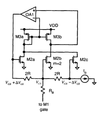
[0021] FIG. 4 is an exemplary embodiment of a bias circuit of the present
invention designed to generate the input bias voltage at which the 2nd-order
nonlinearity is zero.
[0022] FIG. 5 is an alternative embodiment of a bias circuit of the present
invention designed to generate the input bias voltage at which the 3rd-order
nonlinearity is zero.
DETAILED DESCRIPTION OF THE PREFERRED EMBODIMENTS
[0023] The present invention describes a method and bias circuit to
selectively
reduce the 2nd-order or 3rd-order nonlinearities of a transistor and the
corresponding signal distortions. The techniques described herein operates
satisfactorily in spite of process variations from one circuit to another and
temperature fluctuations.
CA 02444700 2003-10-17
WO 02/087072 PCT/US02/12190
[0024] The principles of the present invention are based on the fact that, for
many transistors, the 2nd-order and 3rd-order expansion coefficients of the
output current (i.e., g~ and g3) depend on the input bias voltage. That is,
the
AC output current iD of Equation (5) is a power series comprising 2nd-order
and 3rd-order nonlinearities characterized by the 2nd-order and 3rd-order
expansion coefficients, g~ and g3, respectively. In turn, the value of the
expansion coefficients g2 and g3 depend on the input bias voltage. This
dependence is such that, at a particular input bias voltage, either g~ or g3
1S
zero. If the amplifier input is biased at this voltage, its 2nd or 3rd-order
nonlinearity will be cancelled and the signal will not exhibit the 2nd Or 3rd-
order distortion.
[0025] As an example, consider the transistor circuit of FIG. 1A and its
equivalent circuit, illustrated in FIG. 1B. As previously noted, the drain
current ID is a function of the gate-to-source voltage Vcs. The transfer
characteristic of a short-channel NMOS transistor is illustrated in FIG. 3A
where the drain current ID is plotted as a function of the gate-to-source
voltage
Vcs. FIGS. 3B-3D are graphs of the expansion coefficients gl-g3, derived
from Equation (4b). FIG. 3B illustrates the linear transconductance of the
transistor M1. FIG. 3C illustrates the coefficient of the 2nd-order
nonlinearity.
It should be noted that the expansion coefficient g2 and the corresponding 2nd-
order distortion are zero at Vcs=1.63V. FIG. 3D illustrates the coefficient of
the 3rd-order nonlinearity of the transistor M 1. It should be noted that the
expansion coefficient g3 and the corresponding 3rd-order distortion are zero
at
Vcs=0~~4V .
[0026] Using techniques known in the prior art, it is possible to use a
conventional resistive divider to bias the transistor M 1 with a fixed DC
CA 02444700 2003-10-17
WO 02/087072 PCT/US02/12190
9
voltage. For example FIG. 3D illustrates that a bias voltage of approximately
0.74 volts results in a value of 0 for the expansion coefficient g3. However,
it
should be appreciated that the characteristic curves of FIGS. 3A-3D represent
a single NMOS transistor at a specific temperature. Temperature fluctuations
and drifts in the manufacturing process of the transistor cause these
characteristics to shift relative to the VAS axis. The steep slope of the g3
characteristic in FIG. 3D near the zero-crossing point illustrates that even
minor shifts in this point will increase the 3rd-order distortion
significantly if
the bias voltage remains fixed at 0.74 volts. Accordingly, fixed DC bias
voltage circuits known in the art are inadequate to achieve a stable reduction
or elimination of the 2nd-order or 3'd-order distortion. It is challenging to
design a bias circuit that automatically generates and maintains the optimum
bias voltage that cancels a selected nonlinearity under fluctuating
temperature
and drifting process conditions. The present invention addresses this
challenge.
[0027] To generate and automatically maintain the optimum bias voltage
resulting in zero 2nd or 3rd-order distortion, a bias circuit should have a
replica
of the amplifying transistor such as the bias transistor M2 in FIG. 2 and the
means to produce a measurable electrical quantity such as a DC voltage or
current proportional to g2 or g3 of the replica-transistor. It should also
have a
DC feedback that senses this quantity and automatically adjusts the bias
voltage of both the amplifying transistor and its replica for g2=0 or g3=0.
[0028] The insight into how to generate the DC voltage or current proportional
to g2 or g3 can be gained if equations (4b) are rewritten in terms of small
deviations of the voltages and currents rather than the derivatives.
CA 02444700 2003-10-17
WO 02/087072 PCT/US02/12190
1 Dcvcs+ev~s /z) - I Dcvcs-eves /z)
$ i (vcs ) _ (6a)
Ovcs
1 $uv~S+ev~slz) - $uvcs-ev~slz)
$z (Vcs ) = 2 OVcs
1 I pcv~s+ev~s) - I Dcvcs) _ I Dcv~s) - I pcv~s-ev~s) (6b)
20VGS OVGS wcS
_ 1 1
20V~S ~ID(v~s+ev~s) +ID(v~s-ev~s) -21D(vcs)I
1 $z(v~s+ev~Slz) -$z(v~s-ev~s/z)
$s (vcs ) = 3 OVcs
I D(Vcs+3eVcs /z) 2ID(Vcs+eVcs /z) '~' I D(Vcs-eVcs l2)
2w~s (6c)
3~VGS ID(Vcs+eVcslz) ZID(VcsWVcsl2) +ID(Vcs-3eVcsl2)
20VcS
1 LID(vcs+3ev~slz) +31D(vcs-nv~slz)~
3
60Vcs - ~31 D(vcs+ev~s I z) + I D(Vcs-3eVcs /z)
[0029] It should be noted that terms within the parentheses in equations (6a-
6c) indicate operating parameters. For example, the term IDw~s+e~U.s) in
equation (6b) is intended to indicate the current ID at the voltage Vas +
dV~s.
Similarly, the term I Dw~s+3ev~s l2) in equation (6c) indicates the current to
at a
voltage Vas + 3dV~sl2. The term dVGS is a small deviation from Vas. The
terms in the braces of equations (6b) and (6c) are measurable quantities that
should be set to zero for g2=0 or g3=0 to cancel the 2°d-order or 3rd-
order
distortion, respectively. FIG. 4 illustrates one example of bias circuit that
CA 02444700 2003-10-17
WO 02/087072 PCT/US02/12190
11
generates the term in the braces of (6b) and automatically adjusts Vas to set
this term to zero.
[0030] Transistors M2a, M2b and M2c are replicas of the transistor M1 in
FIG. 1 having the same gate length as M1, but their width is scaled down.
The gates of the three replicas are biased through a resistor chain 2R,2R with
a current sink Io. The resistor unit value R and the current value to are
chosen
such that the voltage drop I~R is equal to dV~sl2 in equations (6a)-(6c). The
value of each resistor in FIG. 4 is selected 2R so that the voltage drops are
conveniently measured in terms of dVGS.
[0031] The circuit of FIG. 4 operates satisfactorily so long as the value for
dV~s is much smaller than the value for Vas to make sure that Vas+dV~s and
VGS-dV~s are close to Vas. For example, if IO were selected to have a value of
0.05 milliamps (mA) and 2R were selected at 400 SZ, the value of dV~s = 20
millivolts. The actual value for d Vas is a design choice within the scope of
the knowledge of the circuit designer using the principles described herein.
Accordingly, the present invention is not limited by the specific current
value
lo, the resistor unit value R or the selected value for dV~s.
[0032] All three bias transistors (M2a, M2b and M2c) have the same W/L
ratio. The transistors M2a and M2c are single transistor devices, while the
transistor M2b consists of two parallel devices, each of which is the same
size
as the transistors M2a and M2c. This is indicated in the circuit of FIG. 4 by
the designation m=2 associated with the transistor M2b where m is the
multiplicity factor.
[0033] The transistor M2a generates the current represented by the first
summand shown in the braces of equation (6b). That is, the transistor M2a
generates a current having the value equal to Io~,,GS+ov~S~. In contrast, the
CA 02444700 2003-10-17
WO 02/087072 PCT/US02/12190
12
transistor M2c generates the current represented by the second summand
shown in the braces of Equation (6b). That is, the transistor M2c generates a
current having the value equal to 1 p~~~s-o~~s) . Finally, the transistor M2b
generates the current represented by the third summand shown in the braces
of the Equation (6b). That is, the transistor M2b generates a current equal to
21D wcs>~
[0034] The currents of the transistors M2a and M2c are added by connecting
their drains together. The common drain of the transistors M2a and M2c and
the drain of M2b are biased through a current mirror comprising a pair of
transistors M3a and M3b where M3a and M3b are PMOS transistors of an
equal size. The differential DC voltage between the drains of the transistors
M3a and M3b is the DC signal proportional to the mathematical term in the
braces of the Equation (6b) and, thus, to the 2°d-order expansion
coefficient
g2. If the differential voltage is zero, the combined current of the
transistors
M2a and M2c is equal to the current of the transistor M2b, and the term in the
braces of the Equation (6b) is zero. The transistor M3b is a current mirror
that produces the same current as the transistor M3a provided that its drain
voltage is the same as that of M3a.
[0035] This balance of the currents is ensured by an operational amplifier
OA1 in FIG. 4 that senses the differential DC voltage between the drains of
the transistors M3a and M3b and generates the input voltage for the resistor
chain 2R, 2R thus creating a feedback loop. The function of the operational
amplifier OA1 is readily understood by a circuit designer following the
example circuit of FIG. 4. Briefly, the operational amplifier OA1 amplifies
the differential input voltage with a high gain and feeds the amplified
voltage
to the gates of the transistors M2a, M2b and M2c with a polarity such that the
CA 02444700 2003-10-17
WO 02/087072 PCT/US02/12190
13
operating point of these transistors is adjusted until their drain voltages
are
equal.
[0036] The gate and drain of the transistor M3a are coupled together. The
positive input of the operational amplifier OA1 is coupled to the junction of
the drains of the transistors M3b and M2b. If, by way of example, the drain
voltage of the transistor M3b increases, the output of the operational
amplifier
OA1 provides an increased signal directly to the gate of the transistor M2a
and to the gates of the transistors M2b and M2c via the resistor network 2R,
2R. The increased gate voltage of the transistor M2b causes a decrease in its
drain voltage thus bringing the drain voltage of the transistor M3b into
equilibrium with its gate voltage which is also the voltage on the gate and
drain of the transistor M3a. Therefore, the drain currents of the transistors
M3a and M3b are maintained equal.
[0037] Thus, the voltage VAS in FIG. 4 is the desired bias voltage that will
eliminate the contribution of the 2nd-order nonlinearity (i.e., ga=0). The
bias
voltage is provided to the gate of the transistor M 1 (see FIG. 1 a) through a
transistor Rb, which serves to isolate the bias circuit from the transistor M1
at
the operating frequency. In an exemplary embodiment, the isolation transistor
Rb may have a value of approximately lOkS2. The feedback loop in FIG. 4
automatically maintains VAS supplied to the gate of M1 in FIG. la at the level
that causes its 2nd-order nonlinearity to be zero even in the presence of
process
and temperature variations.
[0038]The circuit of FIG. 4 selectively generates currents proportional to the
components of the 2nd-order nonlinearity that are used to generate the bias
voltage to effectively cancel out the 2nd-order nonlinearity. A similar
approach may be used to cancel out the 3rd-order nonlinearity. FIG. 5
CA 02444700 2003-10-17
WO 02/087072 PCT/US02/12190
14
illustrates an exemplary embodiment of a circuit that effectively cancels out
the mathematical term in the braces of equation (6c) thus setting the value of
the expansion coefficient g3 equal to zero.
[0039]Although the circuit of FIG. 5 operates in a similar fashion to that of
FIG. 4, some additional explanation may assist in a further understanding of
the operation. An analysis of equation (6c) indicates that there are four
summands contained within the braces. Each of the transistors M2a, M2b,
M2c and M2d in FIG. 5 generates a DC current represented by a respective
summand in the braces of equation (6c). The transistors M2a, M2b, M2c and
M2d are replicas of the transistor M1 in FIG. 1 having the same gate length as
M1, but their width is scaled down. The gates of the four replicas are biased
through the resistor chain 2R,R,R,2R with the current sink Io.
[0040]The voltage drop produced by passing the current Io through the
resistance R is equivalent to dV~sl2 in equations (6a)-(6c). This voltage drop
is chosen relatively small so that Vas+3dVGSl2 and VGS-3dVGSl2 are close to
VGS. As previously discussed, the only requirement is that d Vas be much
smaller than Vas. Similarly, the values for the resistors R and 2R may be
selected as a matter of engineering choice to have convenient resistor values.
The value of the current sink to is also chosen as a matter of design choice
based on the description provided herein. For example, if the circuit of the
present invention is intended for use in a battery operated circuit, it is
desirable to minimize the current draw in the current sink to and power
consumption within the resistors R and 2R for the selected d VGS. In contrast,
a circuit having an external power supply has no such limitations.
Accordingly, the present invention is not limited by the specific values
CA 02444700 2003-10-17
WO 02/087072 PCT/US02/12190
selected for the resistors R and 2R or the value of the current through the
current sink lo.
[0041] All four transistors have the same W/L ratio. However, the transistors
M2a and M2d are single transistor devices while the transistors M2b and MZc
each consist of three parallel devices of the same size as the transistors M2a
and MZd. This is indicated in the circuit of FIG. 5 by the designation m=3
associated with the transistors M2b and M2c.
[0042] The transistor M2a generates the current represented by the first
summand shown in the braces of equation (6c). That is, the transistor M2a
generates a current equal to Io~~s=~.3dVgs l2)' The transistor M2b generates
the
third current shown in the braces of equation (6c). That is, the transistor
M2b
generates the current equal to 3lowgs+ov8, ~z)- The transistor M2c generates
the
second current shown in the braces of equation (6c). That is, the transistor
M2c generates a current equal to 3lDwgg-4Vg,12)' Finally, the transistor M2d
generates the fourth current shown in the braces of equation (6c). That is,
the
transistor M2d generates current equal to I pegs-3ev8s ~z) -
[0043]The currents of the transistors M2a and M2c are added by connecting
their drains together. The currents of the transistors M2b and M2d are added
in the same way.
[0044]The common drains of the transistors M2a,M2c and the transistors
MZb,M2d are biased through a current mirror comprising transistors M3a and
M3b where the transistors M3a and M3b are PMOS transistors of an equal
size. The differential DC voltage between the drains of M3a and M3b is the
DC signal proportional to the mathematical term in the braces of the Equation
(6c) and, thus, to the 3rd-order expansion coefficient g3. If the differential
CA 02444700 2003-10-17
WO 02/087072 PCT/US02/12190
16
voltage is zero, the added currents through the transistors M2a,M2c and
M2b,M2d are equal, and the term in the braces of equation (6c) is zero.
[0045] This balance of the currents is ensured by the operational amplifier
OA I in FIG. 5, which operates in a manner similar to that of the operational
amplifier OA1 in FIG. 4. Specifically, the operational amplifier OAI in FIG.
senses the differential DC voltage between the drains of the transistors M3a
and M3b and generates the input voltage for the resistor chain 2R,R,R,2R
creating a feedback loop. This feedback loop automatically maintains Vas
supplied to the gate of M1 in FIG. 1a at the level that causes its 3rd-order
nonlinearity to be zero even in the presence of process and temperature
variations.
[0046] Thus, the present invention permits a simple approach that achieves a
significant reduction in either the 2nd-order or 3ra-order nonlinearity and
exhibits low sensitivity to variations in the processes used to manufacture
transistors and temperature variations. Although the exemplary bias circuits
of FIG. 4 and FIG. 5 do add additional circuitry, the DC current increase
required to operate the bias circuits of the present invention is negligible.
This is a significant advantage in battery operated applications. Furthermore,
the bias circuits of the present invention do not degrade other circuit
performance, such as the noise figure of the transistor M1 (see FIG. 1A).
Furthermore, the DC bias circuits of the present invention may be used for
transistors (e.g., the transistor M1 of FIG. 1A) operating at virtually any
frequency.
[0047] The described bias circuits are possible embodiments of the invention.
There are other bias circuit topologies that can generate the optimum bias
voltages based on zeroing a DC voltage or current proportional to the 2nd Or
CA 02444700 2003-10-17
WO 02/087072 PCT/US02/12190
17
3ra-order expansion coefficient. The invention can be used in MOSFET,
MESFET, HEMT, BJT and HBT gain stages operating at any frequency.
[0048] It is to be understood that even though various embodiments and
advantages of the present invention have been set forth in the foregoing
description, the above disclosure is illustrative only, and changes may be
made in detail, yet remain within the broad principles of the invention.
Therefore, the present invention is to be limited only by the appended claims.