Note: Descriptions are shown in the official language in which they were submitted.
CA 02445806 2003-10-27
WO 03/045559 PCT/US02/17957
1
DESCRIPTION
Microfluidic Devices with Distributin-Inputs
Statement Of Related Applications)
This application claims priority to U.S. Provisional Patent Application Serial
No.
60/296,897, filed June 7, 2001 and currently pending; and U.S. Provisional
Patent
Application Serial No. 60/357,683, filed February 13, 2002 and currently
pending. Body
Text First Indent
Field Of The Invention
The present invention relates to microfluidic devices and methods for their
use and
manufacture. These devices and methods are useful in performing multiple
microfluidic
scale chemical and biological analyses,in parallel on a single device.
Background Of The Invention
There has been a growing interest in the manufacture and use of microfluidic
systems for the acquisition of chemical and biological information. In
particular, when
conducted in microfluidic volumes, complicated biochemical reactions may be
carried out
using very small volumes of liquid. Among other benefits, microfluidic systems
improve
the response time of reactions, minimize sample volume, and lower reagent
consumption.
When volatile or hazardous materials are used or generated, performing
reactions in
microfluidic volumes also enhances safety and reduces disposal quantities.
Traditionally, microfluidic devices have been constructed in a planar fashion
using
techniques that are borrowed from the silicon fabrication industry.
Representative systems
are described, for example, in some early work by Manz et al. (Trends in Anal.
Chem.
(1990) 10(5): 144-149; Advances in Chromatography (1993) 33: 1-66). In these
publications, microfluidic devices are constructed by using photolithography
to define
channels on silicon or glass substrates and etching techniques to remove
material from the
substrate to form the channels. A cover plate is bonded to the top of the
device to provide
closure. Miniature pumps and valves can also be constructed to be integral
(e.g., within)
such devices. Alternatively, separate or off line pumping mechanisms are
contemplated.
More recently, a number of methods have been developed that allow microfluidic
devices to be constructed from plastic, silicone or other polymeric materials.
In one such
method, a negative mold is first constructed, and plastic or silicone is then
poured into or
over the mold. The mold can be constructed using a silicon wafer (see, e.g.,
Duffy et al.,
CA 02445806 2003-10-27
WO 03/045559 PCT/US02/17957
2
Analytical Chemistry (1998) 70: 4974-4984; McCormick et al., Analytical
Chemistry
(1997) 69: 2626 -2630), or by building a traditional injection molding cavity
for plastic
devices. Some molding facilities have developed techniques to construct
extremely small
molds. Components constructed using a LIGA technique have been developed at
the
Karolsruhe Nuclear Research center in Germany (see, e.g., Schomburg et al.,
Journal of
Micromechanical Microengineering ( 1994) 4: 186-191 ), and commercialized by
MicroParts (Dortmund, Germany). Jenoptik (Jena, Germany) also uses LIGA and a
hot-
embossing technique. Imprinting methods in PMMA have also been demonstrated
(see,
Martynova et.al., Analytical Chemistry (1997) 69: 4783-4789) However, these
techniques
do not lend themselves to rapid prototyping and manufacturing flexibility.
Additionally,
the foregoing references teach only the preparation of planar microfluidic
structures.
Moreover, the tool-up costs for both of these techniques are quite high and
can be cost-
prohibitive.
Various conventional tools and combinations of tools are used for separations
and
detections when performing analyses in conventional macroscopic volumes. Such
tools
include, for example: filters, metering devices, columns, valves, sample
injectors, heaters,
coolers, mixers, splitters, diverters, and electrodes (such as are used to
induce
electrokinetic flow and to perform electrophoretic separations). Attempts to
conduct
separations or detections in microfluidic volumes have been stifled by
difficulties such as
making such tools in microfluidic scale and then integrating such tools into
microfluidic
devices. Another difficulty is accurately measuring stoichiometric
microfluidic volumes
of reagents and solvents to perform analyses on a microfluidic scale.
Additionally,
difficulties in rapidly prototyping microfluidic devices are compounded by
attempts to
incorporate multiple analytical tools.
A particular challenge that has arisen in the design and fabrication of
microfluidic
devices is the proliferation of inputs and outputs associated with such
devices. For
example, PCT Patent Application WO 99/19717, entitled "Laminate Microstructure
Device and Methods for Making Same," by Aclara Biosciences, Inc. (the "Aclara
Application") discloses a microfluidic device, which includes multiple
microfluidic
structures therein. FIG. 1 illustrates a device 100 similar to that disclosed
in the Aclara
Application. The device 100 includes eight microfluidic structures 102A-102H.
Each of
the microfluidic structures 102A-102H has eleven input/output ("I/O") ports
103A-103N.
Consequently, operation of the device 100 would require eighty-eight I/0
connections.
Furthermore, it is anticipated that microfluidic devices may include
substantially more
than eight microfluidic structures per device. Thus, the number of I/O
connections for a
more feature-dense device could be significantly higher than eighty-eight.
CA 02445806 2003-10-27
WO 03/045559 PCT/US02/17957
3
One benefit of microfluidic devices is the ability to perform multiple
experiments
in a small area. The large number of I/O connections required by the device
100 would
have a tendency to either expand the size of the device to accommodate the
connections or
complicate fabrication and operation of the device. In particular, providing a
large number
of I/O connections in a compact area elevates the likelihood of fabrication
and/or
operational errors.
The microfluidic devices described herein may include any number of parallel
functional features and related inputs and outputs. Although the prior art and
illustrative
embodiments of the invention shown herein each have a particular number of
such
features, such features are numbered and lettered to reflect the fact that
additional such
features may be included. For example, in FIG. 2A, the functional features are
numbered
106A-106N, where "N" represents the total number of such features included in
the device
104. Whereas in the illustrated device 104 the "N" represents the third such
functional
feature, such a device 104 could include tens, hundreds or even more of such
functional
features providing the desired functionality according to the invention.
FIGS. 2A-2E use simplified block diagrams to illustrate various permutations
of
desirable microfluidic devices and difficulties created by the need for
multiple I/O
connections. FIG. 2A is a simplified representation of a device 104 similar.
to that shown
in FIG. 1. The device 104 includes a plurality of functional features 106A-
106N. A
functional feature can be any structure for performing a desired fluidic
operation,
including, but not limited to one or more mixers, reactors, separation
chambers, and any
combinations thereof. Each functional feature 106A-106N has a sample input
108A-108N
and an output 108A'-108N'. In addition, each functional feature 106A-106N may
have a
plurality of reagent inputs 110A-110N, 112A-112N, 114A-114N. For simplicity,
the
device 104 is shown with only one sample input, one output, and three reagent
inputs for
each functional feature 106A-106N; however, any number of inputs and outputs
for
samples and reagents may be used as necessitated by the desired fluidic
function to be
performed by the functional feature. Accordingly, the number of I/O
connections required
by such a device 104 equals the number of I/O connections per functional
feature
multiplied by the number of functional features.
If the functional features 106A-106N perform substantially identical
operations in
parallel, then it is likely that the same set of reagents will be used in each
of the functional
features. If the device 104 is used to perform parallel operations using the
same reagents
on a variety of samples, then the number of I/O connections may be reduced if
inputs for
reagents common to more than one functional feature are combined, as shown in
FIG. 2B.
A device 120 includes a plurality of functional features 122A-122N. Each
functional
CA 02445806 2003-10-27
WO 03/045559 PCT/US02/17957
4
feature 122A-122N has a sample input 124A-124N and an output 124A'-124N'. Two
common reagent inputs 126, 128 provide reagents to the functional features
122A-122N.
Because reagent can be provided to all functional features 122A-122N from the
two inputs
126, 128, the total numbers of I/O connections for reagents can be reduced by
(N-1) x Y,
where "N" is the number of functional features and "Y" is the number of
reagent inputs
per functional feature. Thus, if the device 120 includes eight functional
features with two
reagent inputs for each, this approach would result in only two common reagent
inputs,
rather than the sixteen independent reagent inputs that would be required for
a device such
as that shown in FIG. 2A.
The techniques used to fabricate microfluidic devices typically rely on
machining
or etching the surface of a planar material to produce the desired
microfluidic structure.
As a result, these microfluidic structures typically are provided in a single
plane. One
consequence of this approach is that it becomes difficult, if not impossible,
to substantially
expand the functionality and complexity of the fluidic operations due to
structural
limitations. For example, as shown in FIG. 2B, the addition of a third common
reagent
input 130 (shown in ghosted lines) and channels 132, 134 to carry reagent from
the input
130 to the functional features 122A-122N results in the intersection (or
"chanxiel
crossing") of these channels 132, 134 with other reagent channels 136, 138 at
intersection
points 140, 142. Because these structures all are defined in a single plane,
the channel
crossings 132, 134, 136, 138 will result in unintended combining of the
reagents,
essentially rendering the device 120 inoperable for most scientific purposes.
Likewise, as
shown in FIG. 2C, a plurality of reagent inputs 150A-150N may be used to
provide
reagents to two functional features 152A, 152B in a device 149. If, however,
further
functional features 152N are added, channels 154A-154N from any reagent input
150A
1 SON in excess of two will result in problematic channel crossings 156A-156N.
Thus, in a two dimensional device, it is impossible to use of more than two
common non-intersecting reagent inputs when more than two functional features
are used.
Likewise, the use of more than two functional features is impossible when more
than two
common non-intersecting inputs are used. Of course, it may be possible to use
small hoses
to allow crossing lines to "jump over" the intersection. However, such an
approach would
substantially increase the manufacturing complexity of such a microfluidic
device as well
as compound the likelihood of component failures that could render the device
inoperable.
The use of common inputs, while potentially simplifying the I/O connections to
a
microfluidic device, also may create additional problems. As a result of the
very small
dimensions of microfluidic structures, fluids moving through such structures
are
characterized by very low Reynolds Numbers (corresponding to laminar flow) and
flow
CA 02445806 2003-10-27
WO 03/045559 PCT/US02/17957
dynamics that are heavily affected, if not dominated, by surface interactions.
Thus, fluids
in microfluidic structures often exhibit surprising and unexpected properties.
For
example, when fluid traveling through a microfluidic structure encounters a
split or fork in
a channel, the fluid may flow through only one fork or only the other - not
dividing and
5 distributing evenly between the two, as would be expected in conventional
macrofluidic
systems. Alternatively, the flow may split, but not evenly. As a consequence
of this
behavior, it may be difficult to consistently and accurately divide and
distribute a reagent
stream to a plurality of functional features, simply because it may be
difficult to predict
the particular flow paths that will be adopted by a given fluid flowing within
a multi-path
microfluidic structure.
It has been observed that fluid flow behavior within microfluidic structures
may be
influenced by the fluidic impedance encountered by the fluid. The presence and
magnitude of fluidic impedance depends on a number of factors, such as
interaction
between the fluid and the surface of the structure ("surface interactions");
the pressure
driving the fluid ("fluid pressure"); the pressure resisting fluid flow
("backpressure"); the
physical arrangement of the microfluidic structure ("structural geometry");
and the
characteristics of the fluid, including, but not limited to, mass, density,
and viscosity
("fluid properties"). In particular, it has been noted that fluids divided and
distributed
from a single source or inlet (which may be a port, aperture or channel) into
a plurality of
branch channels tend to split evenly among the branch channels only when the
impedance
encountered by the fluid is substantially the same across all of the branch
channels into
which the fluid is being divided.
Thus, if a common input is used to divide and distribute a fluid among
multiple
functional features, care must be taken to match the impedance of each channel
carrying
reagent from the common input to each of the functional features. For example,
FIG. 2D
illustrates a simple microfluidic device 170 having two functional features
172A-172B.
Each of the functional features 172A-172B has a sample input 174A-174B and an
output
176A-176B. Two common reagent inputs 178A, 178B provide reagent to the
functional
features via reagent channels 180A-180D. In this simple configuration,
impedance
matching among channels 180A-180D is provided by positioning the reagent
inputs 178A-
178B equidistantly from the functional features 172A-172B, thereby matching
the length
of each of the channels 180A-180D to each other. So long as such a simple
arrangement
is possible, this approach may provide the desired results. However, as a
design becomes
more complex, due to, for example, increased feature density or input
positions required to
maintain compatibility to a particular laboratory device, such careful
positioning of
reagent inputs may not be possible. Thus, as shown in FIG. 2E, in a device
190, having
CA 02445806 2003-10-27
WO 03/045559 PCT/US02/17957
6
two functional features 191A-191B and common reagent inputs 192A-192B, it may
be
necessary to provide convoluted reagent channels 194A-194D. The convolutions
of the
reagent channels 194A-194D allow the channels 194A-194D to be the same length
(therefore having substantially the same impedance, assuming that the other
channel
characteristics are constant) even though the reagent inputs 192A-192B are not
equidistant
from each of the functional features 191 A-191 B.
If the feature density increases substantially, however, the convolutions
required to
provide the desired impedance matching may become very complex, thereby
complicating
the design, fabrication, operation and validation of the device. Furthermore,
any such
device remains constrained by the channel intersection problem described
above.
In addition, the vast array of microfluidic tools and designs available today
and
anticipated in the future can present an infinite number of I/0 interface
configurations.
For example, in each of the examples described above it can be seen that the
pattern of
inputs and outputs for samples and reagents differs substantially from device
to device.
Moreover, in order to maintain impedance matching among common inputs and/or
to
avoid undesirable channel intersections, the actual positioning of these
inputs and outputs
may be driven by the function of the device rather than the interface of
existing laboratory
tools. Thus, connection of highly parallel microfluidic devices to existing
tools may
require customized interfaces and/or complexes of flexible tubing to allow
connection to
other devices andlor laboratory tools and instruments. Such interface
requirements tend to
enlarge the footprint of the device, complicate operation, complicate
manufacture of the
device andlor increase the complexity of other devices used in conjunction
with the
device.
Thus, it would be desirable to provide microfluidic devices with minimal
numbers
of I/O connections. It also would be desirable to provide microfluidic devices
that
accurately and reliably divide and distribute fluitlic inputs to the various
structures within
the device. It also would be desirable to provide microfluidic devices that
readily interface
with existing laboratory tools.
Summary Of The Invention
In a first separate aspect of the present invention, a mufti-layer
microfluidic device
includes: a plurality of device layers defining at least three functional
features; a first, a
second, and a third distributing input, each associated with each of the at
least three
functional features; and a channel crossover region. The channel crossover
region
includes: a first distribution channel (the first distribution channel defined
in a first device
layer); a second distribution channel (the second distribution channel defined
in a second
CA 02445806 2003-10-27
WO 03/045559 PCT/US02/17957
device layer); and a third device layer disposed between the first device
layer and the
second device layer. The third device layer prevents fluid communication
between the
first channel and the second channel at the channel crossover region.
In another separate aspect of the invention, a mufti-layer microfluidic device
includes at least three functional features, at Least three distributing
inputs each having a
plurality of channels, a plurality of channel crossings, and an intervening
device layer.
Each distributing input is in fluid communication with the functional
features. The
intervening device layer preventing fluid communication between any of the
distributing
inputs at any channel crossing.
In another separate aspect of the invention, a mufti-layer microfluidic device
includes a functional device layer defining at least three functional
features. A first device
layer has a first set of distribution channels in fluid communication with the
functional
features. A second device layer has a second set of distribution channels in
fluid
communication with the functional features. A third device layer has a third
set of
distribution channels in fluid communication with the at least three
functional features.
The second device layer is disposed between the first device layer and the
third device
layer.
In another separate aspect of the invention, a mufti-layer microfluidic device
comprises a first device layer defining at least three functional features and
a first
distributing input in fluid communication with each of the at least three
functional
features. A second device layer defines a second distributing input in fluid
communication with each of the at least three functional features. A third
distributing
input, defined one of the first device layer or the second device layer, is in
fluid
communication with each of the at least three functional features. A third
device layer is
disposed between the first device layer and the second device layer.
In another separate aspect of the invention, any of the foregoing separate
aspects
may be combined for additional advantage. These and other aspects and
advantages of
the invention will be apparent to the skilled artisan upon review of the
following
description, drawings and claims.
Brief Description Of The Drawings
FIG. 1 is a top view of a microfluidic device of the prior art.
FIG. 2A is a block diagram illustrating a planar, two-dimensional microfluidic
device having multiple independent inputs and multiple functional features.
FIG. 2B is a
block diagram illustrating a planar, two-dimensional microfluidic device
having multiple
independent inputs, two common inputs, and multiple functional features. FIG.
2C is a
CA 02445806 2003-10-27
WO 03/045559 PCT/US02/17957
g
block diagram illustrating a planar, two-dimensional micrbfluidic device
having
independent inputs, multiple common inputs, and two functional features. FIG.
2D is a
block diagram illustrating a planar, two-dimensional microfluidic device
having
independent inputs, two impedance-matched common inputs, and two functional
features.
FIG. 2E is a block diagram illustrating a planar, two-dimensional microfluidic
device
having independent inputs, two impedance-matched common inputs, and two
functional
features.
FIG. 3 is a block diagram illustrating the operation of a mufti-layer, three-
dimensional microfluidic device according to one embodiment of the present
invention.
FIG. 4 is a block diagram illustrating the operation of a mufti-layer, three-
dimensional microfluidic device according to another embodiment of the present
invention.
FIG. 5A is an exploded perspective view of a mufti-layer, three-dimensional
microfluidic device according to another embodiment of the present invention.
FIG. 5B is
a top view of the assembled device of FIG. 5A.
FIG. 6A is an exploded perspective view of a mufti-layer, three-dimensional
microfluidic device according to another embodiment of the present invention.
FIG. 6B is
a top view of the assembled device of FIG. 6A. FIG. 6C is an enlarged top view
of a first
portion of the device of FIGS. 6A-6B. FIG. 6D is an enlarged top view of a
second
portion of the separation device of FIGS. 6A-6B.
FIG. 7A is an exploded perspective view of a mufti-layer, three-dimensional
microfluidic device according to another embodiment of the present invention.
FIG. 7B is
a top view of the assembled device of FIG. 7A.
Detailed Description Of Preferred Embodiments
Definitions
The term "channel" or "chamber" as used herein is to be interpreted in a broad
sense. Thus, it is not intended to be restricted to elongated configurations
where the
transverse or longitudinal dimension greatly exceeds the diameter or cross-
sectional
dimension. Rather, such terms are meant to comprise cavities or tunnels of any
desired
shape or configuration through which liquids may be directed. Such a fluid
cavity may,
for example, comprise a flow-through cell where fluid is to be continually
passed or,
alternatively, a chamber for holding a specified, discrete ratio of fluid for
a specified ratio
of time. "Channels" and "chambers" may be filled or may contain internal
structures
comprising, for example, valves, filters, and similar ,or equivalent
components and
materials.
CA 02445806 2003-10-27
WO 03/045559 PCT/US02/17957
9
The term "distributing input" as used herein refers to a fluidic inlet that
divides and
distributes a fluid among multiple functional features. A distributing input
typically
includes a common fluidic region (e.g., a port, an aperture, or equivalent
structure) and
multiple distribution channels that branch outward from the common fluidic
region.
S The term "functional feature" as used herein refers to any microfluidic
structure
within a microfluidic device that performs an operation on, or permits
interaction with,
fluids introduced into the device. For example, functional features may
include, but are
not limited to, mixers, separation channels, reaction chambers, analysis
windows, and
other useful structures known in the art.
The term "microfluidic" as used herein is to be understood, without any
restriction
thereto, to refer to structures or devices through which fluids) are capable
of being passed
or directed, wherein one or more of the dimensions is less than 500 microns.
The terms "stencil" or "stencil layer" as used herein refers to a material
layer or
sheet that is preferably substantially planar, through which one or more
variously shaped
and oriented channels have been cut or otherwise removed through the entire
thickness of
the layer, thus permitting substantial fluid movement within the layer (as
opposed to
simple through-holes for transmitting fluid through one layer to another
layer). The
outlines of the cut or otherwise removed portions form the lateral boundaries
of
microstructures that are completed when a stencil is sandwiched between other
layers,
such as substrates and/or other stencils. Stencil layers can be either
substantially rigid or
flexible (thus permitting one or more layers to be manipulated so as not to
lie in a plane).
Microfluidic devices eneral~
In an especially preferred embodiment, microfluidic devices according to the
present invention are constructed using stencil layers or sheets to define
channels and/or
chambers. As noted previously, a stencil layer is preferably substantially
planar and has a
channel or chamber cut through the entire thickness of the layer to permit
substantial fluid
movement within that layer. Various means may be used to define such channels
or
chambers in stencil layers. For example, a computer-controlled plotter
modified to accept
a cutting blade may be used to cut various patterns through a material layer.
Such a blade
may be used either to cut sections to be detached and removed from the stencil
layer, or to
fashion slits that separate regions in the stencil layer without removing any
material.
Alternatively, a computer-controlled laser cutter may be used to cut portions
through a
material Iayer. While laser cutting may be used to yield precisely dimensioned
microstructures, the use of a laser to cut a stencil layer inherently involves
the removal of
some material. Further examples of methods that may be employed to form
stencil layers
CA 02445806 2003-10-27
WO 03/045559 PCT/US02/17957
include conventional stamping or die-cutting technologies, including rotary
cutters and
other high throughput auto-aligning equipment (sometimes referred to as
converters).
The above-mentioned methods for cutting through a stencil layer or sheet
permits robust
devices to be fabricated quickly and inexpensively compared to conventional
surface
5 micromachining or material deposition techniques that are conventionally
employed to
produce microfluidic devices.
After a portion of a stencil layer is cut or removed, the outlines of the cut
or
otherwise removed portions form the lateral boundaries of microstructures that
are
completed upon sandwiching a stencil between substrates and/or other stencils.
The
10 thickness or height of the microstructures such as channels or chambers can
be varied by
altering the thickness of the stencil layer, or by using multiple
substantially identical
stencil layers stacked on top of one another. When assembled in a microfluidic
device, the
top and bottom surfaces of stencil layers are intended to mate with one or
more adjacent
layers (such as stencil layers or substrate layers) to form a substantially
enclosed device,
typically having at least one inlet port and at least one outlet port.
A wide variety of materials may be used to fabricate microfluidic devices
having
sandwiched stencil layers, including polymeric, metallic, and/or composite
materials, to
name a few. Various preferred embodiments utilize porous materials including
filter
materials. Substrates and stencils may be substantially rigid or flexible.
Selection of
particular materials for a desired application depends on numerous factors
including: the
types, concentrations, and residence times of substances (e.g., solvents,
reactants, and
products) present in regions of a device; temperature; pressure; pH; presence
or absence of
gases; and optical properties.
Various means may be used to seal or bond layers of a device together. For
example, adhesives may be used. In one embodiment, one or more layers of a
device may
be fabricated from single- or double-sided adhesive tape, although other
methods of
adhering stencil layers may be used. Portions of the tape (of the desired
shape and
dimensions) can be cut and removed to form channels, chambers, and/or
apertures. A tape
stencil can then be placed on a supporting substrate with an appropriate cover
layer,
between layers of tape, or between layers of other materials. In one
embodiment, stencil
layers can be stacked on each other. In this embodiment, the thickness or
height of the
channels within a particular stencil layer can be varied by varying the
thickness of the
stencil layer (e.g., the tape carrier and the adhesive material thereon) or by
using multiple
substantially identical stencil layers stacked on top of one another. Various
types of tape
may be used with such an embodiment. Suitable tape carrier materials include
but are not
limited to polyesters, polycarbonates, polytetrafluoroethlyenes,
polypropylenes, and
CA 02445806 2003-10-27
WO 03/045559 PCT/US02/17957
11
polyimides. Such tapes may have various methods of curing, including curing by
pressure, temperature, or chemical or optical interaction. The thickness of
these Garner
materials and adhesives may be varied.
In another embodiment, device layers may be directly bonded without using
S adhesives to provide high bond strength (which is especially desirable fox
high-pressure
applications) and eliminate potential compatibility problems between such
adhesives and
solvents and/or samples. In one embodiment, multiple layers of 7.5-mil (188
micron)
thickness "Clear Tear Seal" polypropylene (American Profol, Cedar Rapids, IA)
including
at least one stencil layer may be stacked together, placed between glass
platens and
compressed to apply a pressure of 0.26 psi (1.79 kPa) to the layered stack,
and then heated
in an industrial oven for a period of approximately 5 hours at a temperature
of 154 °C to
yield a permanently bonded microstructure well-suited for use with high-
pressure column
packing methods.
Notably, stencil-based fabrication methods enable very rapid fabrication of
devices, both for prototyping and for high-volume production. Rapid
prototyping is
invaluable for trying and optimizing new device designs, since designs may be
quickly
implemented, tested, and (if necessary) modified and further tested to achieve
a desired
result. The ability to prototype devices quickly with stencil fabrication
methods also
permits many different variants of a particular design to be tested and
evaluated
concurrently.
Further embodiments may be fabricated from various materials using well-known
techniques such as embossing, stamping, molding, and soft lithography.
In addition to the use of adhesives and the adhesiveless bonding method
discussed
above, other techniques may be used to attach one or more of the various
layers of
microfluidic devices useful with the present invention, as would be recognized
by one of
ordinary skill in attaching materials. For example, attachment techniques
including
thermal, chemical, or light-activated bonding steps; mechanical attachment
(such as using
clamps or screws to apply pressure to the layers); and/or other equivalent
coupling
methods may be used.
Preferred embodiments
Microfluidic devices according to the invention may be provided to perform any
desirable fluidic operation, including, without limitation, synthesis and
analysis of
chemical or biological species. These microfluidic devices are characterized
by a plurality
of functional features for performing one or more fluidic operations. Each
functional
feature may have independent inputs for introduction of samples, reagents or
other useful
CA 02445806 2003-10-27
WO 03/045559 PCT/US02/17957
12
fluids required to perform the operative functions) of the functional feature.
Independent
outputs allow products of the operations) to be analyzed, collected, disposed
of, or
transferred to other functional features, laboratory instruments, or other
desirable
locations. If the product is to be discarded, then the outputs may be merged
into a
common waste channel.
Reagents, samples, or other fluids common to multiple functional features
("common fluids") may be input into a microfluidic device or system through
one or more
distributing inputs that divide and distribute the common fluids as desired.
The use of a
mufti-layer fabrication technique allows multiple such distributing inputs to
distribute to
multiple functional features in a device without undesirable intersection of
fluid channels.
This capability arises as a consequence of the three-dimensional character of
mufti-layer
devices, which allows two or more channels to cross each other with a device
layer
disposed and preventing fluid communication therebetween.
According to one embodiment of the invention, a microfluidic analytical device
provides both separation and detection capabilities. A schematic diagram of
one
embodiment of the present invention is shown in FIG. 3. This schematic diagram
describes a general analytical technique for the current invention. As would
be
appreciated by one skilled in the art, variations on this theme are possible
as certain
individual steps may be rearranged or omitted for particular applications.
Referring to
FIG. 3, a device 400 includes two inlet ports 481, 482 provide solvent to two
regulators
483, 484 that feed a mixer 485. Downstream of the mixer 485 is a separation
chamber
486. A sample inlet port 480 delivers sample to the device 400 between the
mixer 485 and
the separation chamber 486. Alternatively, the sample may be injected within
the
separation chamber 486. In a further alternative embodiment, sample may be
injected
using one of the solvent inlets 481, 482. In another embodiment, the solvent
may be
mixed "off board," necessitating only one solvent inlet. More solvent inlets
can be added
to increase the complexity of the solvent mixture. Moreover, multiple devices
400 may be
combined on a single microfluidic platform so that multiple operations may be
performed
in parallel. When it is desirable to perform the functions provided by the
device 400 in
parallel in a single microfluidic device or system, distributing inputs may be
incorporated
so that solvents and other fluids common to two or more of the parallel
operations may be
introduced into the platform at a single point and distributed to each device
as desired.
The mixing region 485 effectively mixes the solvent before it reaches the
separation chamber 486. The separation chamber 485 can be configured in a
variety of
ways, as would be recognized by one skilled in the art, to perform techniques
such as ion
exchange, gel filtration or size exclusion, adsorption, partition,
chromatofocusing, and
CA 02445806 2003-10-27
WO 03/045559 PCT/US02/17957
13
affinity chromatographies. In one embodiment, the separation chamber 486 is a
straight
channel filled with stationary phase material, The length of the channel may
be varied as
needed to perform the desired separation.
The exit of the separation chamber 486 leads to the initial flow-through
detector
487. Preferably, the detector 487 is external to the device 400.
Alternatively, on-board
detection may be provided. The flow-through detection scheme will typically be
set up so
that molecules or atoms of interest can be detected while the fluid is still
flowing in the
device 400. Examples of the flow-through detectors 487 include but are not
limited to
UV-visible spectroscopy, Raman spectroscopy, fluorescence detection,
chemiluminescence, electrochemical detection, and other electronic detections
such as
capacitive and conductivity measurement.
The flow-through detector 487 may be used to pre-screen the fluid as it comes
off
the separation chamber 486 to determine if the given fluid has molecules of
interest for
further analysis or storage. In FIG. 3, a flow-through detector 487 leads to a
diverter
module 488 which can direct the fluid to a waste chamber 489, a secondary
detector
module 490, or a fraction collector 491. The fraction collector 491 contains
an additional
diverter 492 and a number of collection chambers 493-495. A larger or smaller
number of
collection chambers may be used.
The secondary detector 490 may utilize a destructive detection technology such
as
mass spectrometry, nuclear magnetic resonance, evaporative light scattering,
ion mobility
spectrometry, or immobilization on material such as glycerol or porous silicon
for matrix
assisted laser desorption ionization ("MALDI"). It may be necessary for the
detector 490
to have an off board collection mechanism, such as collection into a vial,
capillary tube,
hose, etc. that leads to the detector 490. Alternatively, a sampling mechanism
can be built
into the microfluidic device so that the sample is directly injected into an
off board
detection system. For example, the outlet of the diverter 488 can Iead to an
open port to
be used for electrospray.
In a preferred embodiment of the present invention, a parallel processing
microfluidic analytical device is constructed. The term "parallel processing"
as used
herein refers to multiple microfluidic systems on a given contiguous device
wherein some
or all of the systems are in fluid communication with one another. In a
preferred
embodiment, multiple fluidic inlets are provided to a parallel processing
microfluidic
device. In another embodiment, multiple outlets, distributing inlets, and/or
detectors are in
communication with more than one microfluidic systems on a given device. In
these
embodiments, a variety of simultaneous analytical processes may be
accomplished using a
small number of control inputs or outputs.
CA 02445806 2003-10-27
WO 03/045559 PCT/US02/17957
14
In another embodiment, a plurality of analytical separation chambers or
channels
reside on a single microfluidic device. This plurality of separation chambers
are
connected to microfluidic inlet ports that are used to insert samples for
separation. The
inlet ports for sample injection and solvent injection can be the same ports
or different
ports. In a preferred embodiment of the invention, the plurality of separation
chambers
axe connected in such a way that a single sample injection port may deliver
fluid to a
plurality of separation chambers. In this manner, sample can be injected at a
single
macroscopic connection but be loaded onto ~a multitude of chambers.
In another embodiment, a multitude of separation chambers can be connected to
a
small number of solvent inlets that simultaneously or serially apply solvent
in known
mixtures to said separation chambers. In this manner, a small number of "off
board"
pumps can be used to control a multitude of separation chambers.
Referring to FIG. 4, a schematic illustrating a parallel processing
microfluidic
analysis system according to one embodiment is shown. The system has
distributing
1 S inputs 510, 511 that are connected to splitters 512, 513. Each splitter is
connected to two
regulators 514-517 for individually regulating the pressure and/or flow of
solvent to each
of the mixers 518, 519. In a preferred embodiment, the regulators 514-517 are
externally
controlled so that the user can specify the mixing ratios of fluids A and B
when they reach
the mixers 518, 519. In another preferred embodiment, the regulators 514-517
are fixed so
that a known constant mixing ratio will be achieved at the outlet of each
mixer module. In
FIG, 4, a sample inlet is not illustrated, but one or more inlets can be
provided in various
locations. In one embodiment, a sample is injected to both separation chambers
520, 521.
In another embodiment, multiple samples are injected. The mixers 518, 519 lead
to two
separation chambers 520, 521. The separation media can be composed of a
variety of
components or single components. Each separation chamber has an individual
flow-
through detector 522, 523. The flow-through detectors may be of various types.
In one
embodiment, off board detectors that scan from one channel to the other are
used. Very
fast scanning can be accomplished with appropriate optics, as will be
recognized by one
skilled in the art.
Alternatively, both channels 522, 523 can be probed simultaneously. This
probing
can be accomplished by various methods such as scanning or splitting a single
light
source, or by providing multiple light sources or other detectors. In a
preferred
embodiment, a non-invasive detection technology (such as UV-visible
absorption) using
off board components is used to probe the fluid immediately past the
separation chambers
520, 521. Then, if a molecule of interest is detected using the off board
detector, the
diverters 524, 525 may send the fluid to a secondary detector 527 (possibly
using
CA 02445806 2003-10-27
WO 03/045559 PCT/US02/17957
destructive methods). Alternatively, if no signal of interest is detected,
then the sample
may be diverted to a waste chamber 526. Other components such as a fraction
collector
could be added.
The embodiment shown in FIG. 4 would allow two pumps to control the solvents
5 for two parallel fluid circuits. To accomplish the same result in a non-
parallel manner,
four pumps would be required. While it is possible to provide and operate
multiple
parallel fluid circuits on a single microfluidic device, as the number of
fluid circuits
increases, it becomes problematic to increase the number of inlet ports,
pumps, and
detectors at the same rate. In many applications, these off board systems are
expensive
10 and large. Thus, if it is desired to simultaneously perform 100
separations, a parallel
device would require 200 inlet ports, 200 pumping systems, 100 waste chambers
and 100
detectors. It is therefore illustrated that the use of distributing inputs
enables simplified
implementation of multiple analyses on a single microfluidic device.
In embodiments described above, a multitude of separation chambers can be
added
15 by simply increasing the number of on-board regulators, splitters, mixers,
and diverters.
These on-board components can be built into the chip and be microfluidic in
nature, if
desirable in a particular application. In this manner, the number of inlet
ports and off
board pumps and detectors remains constant.
While microfluidic tools and devices provided herein have been applied to
perform
analyses, they may also be combined and/or integrated with further tools to
perform
syntheses. Modular or integrated microfluidic devices having regions for
performing
syntheses and analyses are contemplated.
Refernng to FIGS. SA-SB, a mufti-column microfluidic liquid chromatography
(LC) device 1020 was fabricated in eight device layers 1021-1028 using a
sandwiched
stencil construction method. A laser cutter was used to cut and define various
holes and
channels in the layers of the device 1020. The first device layer 1021, made
of IO-mil
(250 micron) thickness polyester film, included injection ports 1029 and
column outlet
ports 1030. The second device layer 1022 was a 5.8-mil (147 micron) double-
sided tape
with a polyester carrier and rubber adhesive to adhere to the first and third
device layers
1021, 1023. The second device layer 1022 included an injection channel 1031
having a
segment perpendicular to the columns 1038 (placed into the fifth device layer
1025), and
vias 1032 connecting to the column outlet ports 1032. Both the third and
fourth device
layers 1023, 1024 included injection vias 1033, 1034 and outlet vias 1035,
1036 in the
same configuration. The second device layer 1022 was a 0.8-mil (20 micron)
polyester
film, and the third, fourth, sixth, and seventh device layers 1023, 1024,
1026, 1027 were
made from 4-mil (100 micron) modified polyolefin thermoplastic adhesive.
Alternatively,
CA 02445806 2003-10-27
WO 03/045559 PCT/US02/17957
16
a thicker thermoplastic adhesive device layer, if available, could be
substituted for the
third and fourth device layers 1023, 1024 (and likewise for the sixth and
device seventh
layers 1026, 1027) to provide enough thermoplastic material to seal any gaps
around the
columns 1038. The fifth device layer 1025 was made of a 10-mil (250 micron)
polyester
film from which several separation channels 1037, each 40-mils wide, were
defined. 40-
mil (1 mm) width strips 1038 of polyester coated with silica gel,
approximately 17 mils
(430 microns) thick including a 250 ~m coating thickness (Whatman Inc.,
Clifton, NJ,
Cat. No. 4410 221) were placed into the respective channels 1037 to serve as
liquid
chromatography stationary phase material. The eighth device layer 1028 was a
rigid
substrate. Gaps around the LC columns 1038 were sealed to prevent leakage by
laminating the thermoplastic layers (the fourth, sixth, and seventh device
layers 1023,
1024, 1026, 1027) around the fifth device layer 1025 using a conventional
pouch-
laminating machine.
Following assembly of all device layers, the device 1020 was re-laminated to
ensure that any spaces around the columns 1038 were filled. Notably, while
only three
separation channels 1037 having stationary phase material 1038 (collectively,
"columns")
are illustrated in the device 1020, other embodiments according to similar
designs may be
easily constructed with a multitude of columns, without any loss of
performance.
1t should be noted, however, that the device 1020, while taking advantage of
the
mufti-layer construction to position fluid channels as desired, does not
provide impedance
matched input channels to each of the separation columns. In another
embodiment of the
present invention, a preferred means of providing substantially the same
impedance
among multiple branch channels is to present to the fluid substantially
identical structural
geometries at any point at which an inlet channel encounters one or more
branch channels
("branching junction"). Thus, a fluid encountering a branching junction will
be directed
into a plurality of branch channels, each presenting a substantially identical
geometric
interface to the inlet channel. The structural geometry includes such factors
as the length
of the branch channel, diameter of the interface, changes in direction and
angle of the fluid
flow, etc. In a preferred embodiment, such substantial identity of structural
geometry may
be provided by means of a topologically symmetrical structure.
FIGS. 6A-6B illustrate a microfluidic separation device 10 constructed with
nine
layers 11-I9, including multiple stencil layers 12-18. Each of the nine layers
11-19
defines two alignment holes 20, 21, which are used in conjunction with
external pins (not
shown) to aid in aligning the layers during construction or in aligning the
device 10 with
an external interface during a packing process. The first layer 11 defines
several fluitlic
ports: two inlet ports 22, 24 are used to admit mobile phase solvent to the
device 10; eight
CA 02445806 2003-10-27
WO 03/045559 PCT/US02/17957
17
sample ports 28A-28N permit sample to be introduced to eight columns (provided
in
channels 45A-45N); a slurry inlet port 26 is used during a column packing
procedure to
admit slurry to the device 10; and a fluidic port 30 that is used (1) during
the packing
process to exhaust (slurry) solvent from the device 10; and (2) during
operation of the
separation device 10 to exit mobile phase solvent,and sample from the device
10 following
separation. The first through sixth layers 11-16 each define eight optical
detection
windows 32A-32N. Defining these windows 32A-32N through these layers 11-16
facilitates optical detection since it reduces the amount of material between
an optical
detector (not shown) such as a conventional UV-VIS detector, and the samples
contained
'in output channel segments 70A-70N downstream of the column-containing
channels 45.
The second through seventh layers 12-17 define solvent vias 22A to transport a
first mobile phase channel 64 defined in the eighth layer 18, with further
solvent vias 24A
defined in the second through fifth layers 12-15 to transport a second mobile
phase solvent
to the channel 46 defined in the sixth layer 16. Further vias 30A are defined
in the second
through sixth layers 12-16 to provide a fluid path between the fluidic port 30
and the
channel 62 defined in the seventh layer 17. A via 26 defined in the second
layer 12
communicates slurry from the slurry inlet port 26 to an elongate channel 38
defined in the
third layer 13 during the slurry packing process along slurry fluid flow paths
73A-73N.
Preferably, particulate material deposited by the slurry packing process fills
the channel 42
and at least a portion of the channel 38. The second layer 12 further defines
eight sample
channels 35A-35N having enlarged regions 34A-34N aligned with the sample inlet
ports
28 defined in the first layer 11.
The third layer 13 defines an elongate channel 38 along with eight sample vias
36
aligned with the ends of the sample channels 35. The fourth channel defines
eight sample
vias 44 aligned with the vias 36 in the third channel 13. A (sample) frit 40
is placed
between the third and fourth layers 13, 14. Although various frit materials
may be used,
the frit 40 (along with frits 50, 51) is preferably constructed from a
permeable
polypropylene membrane such as, for example, 1-mil (25 micron) thickness
Celgard 2500
membrane (55% porosity, 0.209 x 0.054 micron pore size, Celgard Inc.,
Charlotte, NC),
particularly if the layers 11-19 of the device 10 are bonded together using an
adhesiveless
thermal bonding method utilizing platens, such as described above. Applicants
have
obtained favorable results using this specific frit material, without
noticeable wicking or
lateral flow within the frit despite using a single strip of the frit membrane
to serve
multiple adjacent column-containing channels. As an alternative to the single
frit 40,
multiple discrete frits (not shown) of various porous material types and
thickness may be
substituted. The fourth layer 14 fizrther defines a manifold channel 42 that
provides fluid
CA 02445806 2003-10-27
WO 03/045559 PCT/US02/17957
18
communication with the separation channels 45A-45N defined in the fifth layer
15 and the
elongate channel 38 defined in the third layer 13 along fluid flow paths 73A-
73N. The
separation channels 45A-45N are preferably about 40 mils (1 mm) wide or
smaller.
The sixth layer 46 defines a channel 46 that receives a second mobile phase
solvent
S for transport to the slit 52 defined in the seventh layer 17, which
facilitates mixing of the
two solvents in the channel 64 downstream of the slit 52. Further defined in
the sixth
layer I6 are a first set of eight vias 48 for admitting mixed mobile phase
solvent to the
upstream end of the channels 45 and the separation columns contained therein,
and a
second set of eight vias 49 at the downstream end of the same channels 45 for
receiving
mobile phase solvent and sample. Two frits 50, 51 are placed between the sixth
and the
seventh layers 16, 17. The first (mobile phase solvent) frit 50 is placed
immediately above
the first set of eight vias 48, while the second (mobile phase + sample) frit
51 is placed
immediately above the second set of eight vias 49 and below a similar set of
eight vias 60
defined in the seventh layer 17. The seventh layer 17 defines a channel
segment 58, two
medium forked channel segments 68, and eight vias 54 for communicating mobile
phase
solvent through the frit 50 and the vias 48 to the separation columns
contained in the
channels 45A-45N defined in the fifth layer I S. The seventh layer 17 further
defines ~ a
transverse manifold channel 62 that receives mobile phase 'solvent and sample
during
separation, and that receives (slurry) solvent during column packing, for
routing such
fluids through vias 30A to the fluidic exit port 30. The eighth layer 18
defines a mixing
channel 64, one large forked channel segment 68, and four small forked channel
segments
66. The eighth layer 18 further defines eight parallel channel segments 70
downstream of
the frit 51 for receiving (mobile phase) solvent and sample (during
separation) or (slurry)
solvent (during slurry packing), and for transporting such fluids) to the
manifold channel
62 defined in the seventh layer 17. The ninth layer 19 serves as a cover for
the channel
structures defined in the eighth layer 18.
FIG. 6B is a top view of the assembled device 10 of FIG. 6A. FIGS. 6C-6D
provide expanded views of two portions of the device 10. FIG. 6C shows the
sample
injection channels 35A-35N with associated enlarged regions 34A-34N that are
aligned
with the sample inlet ports 28A-28N defined in the first layer 11. For
simplicity, the frit
has been omitted from FIG. 6C, although FIGS. 6A-6B correctly show the frit 40
placed between the sample vias 36, 44 upstream of the point where samples are
injected
onto the separation channels 45A-45N to be filled with particulate column
material. FIG.
6D shows the mixing and splitting channel structures that communicate mobile
phase
35 solvent to the column-containing channels 45A-45N. During operation of the
device 10, a
first mobile phase solvent is injected into a first solvent inlet port 22 and
flows into
CA 02445806 2003-10-27
WO 03/045559 PCT/US02/17957
19
channel 64. A second mobile phase solvent is injected into a second solvent
inlet port 24
and flows through the channel segment 46 through a slit 52 where it is layered
with and
joins the first solvent in the channel 64. The two layered solvents mix in the
channel 64
and subsequent channel segment 58, whereafter the mixed solvent stream is
split into eight
portions or substreams, along fluid flow paths 74A-74N, by way of transport
through a
large forked channel segment 68, two medium forked channel segments 56, and
four small
forked channel segments 66. Alternatively, each solvent could be distributed
by
independent sputters (not shown). Also, the solvents could be mixed in a
mixing chamber
(not shown) before introduction into the separation channels 45A-45N or could
be mixed
in the separate channels. The eight solvent mixture substreams are then
injected through
vias 54 and 48 into the (column-containing) separation channels 45A-45N along
fluid flow
paths 74A-74N. For simplicity, the frit 50 disposed between the vial 54 and 48
have been
omitted in FIG. 6D, although this frit 50 is shown in FIGS. 6A-6B.
Preferably, the various layers 11-19 of the device 10 are fabricated from un-
oriented polypropylene and bonded using an adhesiveless thermal bonding method
utilizing platens, as described above. This construction method yields
chemically resistant
devices having high bond strength, both desirable attributes for withstanding
a column
packing process and subsequent operation to provide separation utility.
While the device 10 illustrated in FIGS. 6A-6D represents a preferred fluidic
device, a wide variety of other fluidic devices may be used. In certain
embodiments,
fluidic devices may include one or more tubes, particularly capillary tubes.
For example,
capillary tubes may be embedded in one or more channels of a microfluidic
device.
In liquid chromatography applications, it is often desirable to alter the
makeup of
the mobile phase during a particular separation. If multiple separation
columns are
provided in a single integrated device (such as the device 10) and the makeup
of the
mobile phase is subject to change over time, then at a common linear distance
from the
mobile phase inlet it is desirable for mobile phase to have a substantially
identical
composition from one column to the next. This is achieved with the device 10
due to two
factors: ( 1 ) volume of the fluid flow paths 74A-74N of each (split) mobile
phase solvent
substream (shown in FIG. 6D) is substantially the same to each column; and (2)
each flow
path 74A-74N downstream of the fluidic (mobile phase and sample) inlets is
characterized
by substantially the same impedance.
The first factor, substantially equal substream flow paths 74A-74N, is
promoted by
design of the mufti-splitter incorporating elements 58, 68, 56, and 66. The
second factor,
substantial equality of the impedance of each column, is promoted by both
design of the
fluidic device 10 and the fabrication of multiple columns in fluid
communication (e.g.,
CA 02445806 2003-10-27
WO 03/045559 PCT/US02/17957
having a common outlet) using a slurry packing method. Where multiple columns
are in
fluid communication with a common outlet, slurry flow within the device is
biased toward
any low impedance region among the flow paths 73A-73N. The more slurry that
flows to
a particular region during the packing process, the more particulate is
deposited to locally
5 elevate the impedance, thus yielding a self correcting method for producing
substantially
equal impedance from one column to the next.
Thus, FIGS. 6A-6D illustrate a mufti-layer device 10 having multiple
functional
features (separation channels 45A-45N, optical detection windows 32A-32N),
independent
inlets and outlets (sample inlet ports 28A-28N, outlet channel segments 70A-
70N), and
10 three distributing inputs (slurry inlet 26, solvent inputs 22, 24). As
discussed above, a
device having three or more functional features and/or three or more common
inputs will
necessarily have channel crossings. The term "channel crossing" as used herein
refers to
the crossing of any fluid carrying features of a device, including, but not
limited to
channels crossing channels, chambers crossing chambers, functional features
crossing
15 functional features, channels crossing chambers, channels crossing
functional features and
any other possible combination. Moreover, a device having three or more
functional
features andlor three or more common inputs, where common fluids must be
divided and
distributed accurately and evenly preferably has impedance-matched input
channels, and
more preferably achieves impedance-matching by means of input channels of
substantially
20 equal length - a state most efficiently achieved with no restriction on
channel crossings or
channel geometry relative to other channels or the overall device.
Thus, by necessity and preference, the device 10 includes numerous charnel
crossings 72A-72N. In the device 10, however, these channel crossings 72A-72N
do not
allow undesirable fluid communication between the channels that cross, because
at least
one device layer is disposed between the crossing channels at these channel
crossings
72A-72N. For example, a sputter channel 68 in device layer 18 crosses a
separation
channel 45B in device layer I S at channel crossing 77A. However, other device
layers 16,
17 are disposed between the device layers 15, I8 in question, thereby
preventing any
undesirable fluid communication between splitter channel 68 and separation
channel 45B
at channel crossing 77A.
FIGS. 6A-6D also illustrate that distributing inputs need not distribute only
samples, solvents, or reagents for the actual fluidic operation to be
performed.
Distributing inputs may be used to pre-treat, charge, load or otherwise
provide structural
or chemical elements of the functional feature - in the case of the device 10,
a distributing
input (i.e., slurry input 26 and the channel 38 and the manifold channel 42)
distributes to
each of the functional features (i.e., separation channels 45A-45N) a
particulate-containing
CA 02445806 2003-10-27
WO 03/045559 PCT/US02/17957
21
slurry that packs the separation channels 45A-45N with the particulate
material. Once the
separation channels 45A-45N are packed and the device is operated, the
particulate matter
effects the separation performed the device 10.
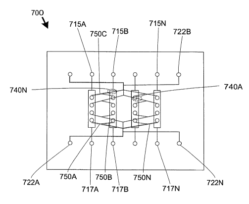
Referring to FIGS. 7A-7B, a microfluidic device 700 for combining fluids is
provided. The device 700 may be used for performing assays, dilutions,
reactions or any
other operation where the combination of two or more fluids is desirable. The
device 700
is constructed from eight device layers 702-709. The first device layer 702 is
a substrate
to support the device 700 and seal the microfluidic structures defined in the
second device
layer 703. The second device layer 703 defines a plurality of functional
features 71 OA
710N, sample inputs 712A-712N, and outputs 714A-714N. The third layer defines
input
vias 716A, output vias 718B and a plurality of reagent vias 720A. The fourth
device layer
705 defines input vias 716B, output vias 718B, a plurality of reagent vias 720
B and a
reagent splitter 724A. The next three device layers 706-708 each define input
vias 716C-
716E, output vial 718C-718E, a plurality of reagent vias 720C-720N and reagent
sputters
724B-724N. The last device layer 709 defines input ports 716N, output ports
718N and
distributing inputs 722A-722N. The last device~layer 709 also seals the device
700. The
functional features 710A-7,lON may be mixers, reactors or any other structures
in which it
is desirable to combine fluids.
In operation, fluid samples are supplied to the device 700 through the input
ports
715A-71 SN. The samples travel through the input vias 716B-716N and into the
functional
features 710A-710N along fluid flow paths 750A-750N (shown as ghosted lines).
Reagents with which the samples are to be mixed are introduced at inputs 722A-
722N,
which travel through vias 720A-720N into the splitters 724A-724N and then into
the
functional features 710A-710N. 1t should be noted that the splitters 724A-724N
are
geometrically symmetrical, thereby insuring that any fluid introduced into
each splitter
724A-724N will divide into four equal portions before being delivered to the
mixing
chambers 710A-71 ON.
The device 700 includes multiple functional features (functional features . 71
OA-
710N), independent inlets and outlets (input ports 715A-715N), and four
distributing
inputs (the combination of inputs 722A-722N, vias 720A-720N and splitters 724A-
724N).
Consequently, for the reasons described above, numerous channel crossings 740A-
740N
are apparent. However, because the device is constructed from multiple layers,
the
channels in question may be defined in non-adjacent layers, whereby any
intervening
layers prevent undesirable fluid communication between the fluid flow paths
750A-750N,
and other channels at features at the channel crossings 740A-740N.
CA 02445806 2003-10-27
WO 03/045559 PCT/US02/17957
22
Moreover, it may be noted that all inputs 722A-722N, 715A-715N and outputs
717A-717N are positioned along two outer edges of the device 10. Because
multiple
device layers 702-709 are used to fabricate the device 10, channel crossings
need not be
avoided, thereby allowing the input and output ports to be positioned anywhere
on the
device 10 suitable to provide compatibility with other devices that might be
used in
conjunction with the device 10. In this embodiment, inputs 722A-722N, 715A-
715N and
outputs 717A-717N are positioned along two outer edges of the device 10;
however, it will
be apparent to one skilled in the art that any desirable positioning of inputs
and outputs
may be selected.
FIGS. 3A-3B, 4A-4B, SA-SB, 6A-6D and 7A-7B illustrate several devices suitable
for providing samples to multiple functional features to be combined with
multiple
reagents. It should be understood that such microfluidic devices may be
modified to
reduce or increase the number of samples and reagents that may be used, simply
by
increasing or decreasing the number of chambers, inputs, splitters and device
layers.
1 S It is to be understood that the illustrations and descriptions of views of
individual
microfluidic tools, devices, and methods provided herein are intended to
disclose
components that may be combined in a working device. Various arrangements and
combinations of individual tools, devices, and methods provided herein are
contemplated,
depending on the requirements of the particular application. The particular
microfluidic
tools, devices, and methods illustrated and described herein are provided by
way of
example only, and are not intended to limit the scope of the invention.