Note: Descriptions are shown in the official language in which they were submitted.
CA 02446874 2011-07-29
54298-7
1
APPARATUS AND METHOD FOR ENCODING AND COMPUTING
A DISCRETE COSINE TRANSFORM USING A BUTTERFLY
PROCESSOR
BACKGROUND OF THE INVENTION
I. Field of the Invention
[0001] The present invention relates to digital signal processing. More
specifically, the present invention relates to an apparatus and method for
determining the
transform of a block of encoded data.
II. Description of the Related Art
[0002] Digital picture processing has a prominent position in the general
discipline of
digital signal processing. The importance of human visual perception has
encouraged
tremendous interest and advances in the art and science of digital picture
processing. In
the field of transmission and reception of video signals, such as those used
for projecting
films or movies, various improvements are being made to image compression
techniques.
Many of the current and proposed video systems make use of digital encoding
techniques. Aspects of this field include image coding, image restoration, and
image
feature selection. Image coding represents the attempts to transmit pictures
of digital
communication channels in an efficient manner, making use of as few bits as
possible to
minimize the band width required, while at the same time, maintaining
distortions within
certain limits. Image restoration represents efforts to recover the true image
of the
object. The coded image being transmitted over a communication channel may
have
been distorted by various factors. Source of degradation may have arisen
originally in
creating the image from the object. Feature selection refers to the selection
of certain
attributes of the picture. Such attributes may be required in the
recognition,
classification, and decision in a wider context.
[0003] Digital encoding of video, such as that in digital cinema, is an
area which benefits
from improved image compression techniques. Digital image compression may be
CA 02446874 2011-07-29
54298-7
2
generally classified into two categories: loss-less and lossy methods. A loss-
less image is
recovered without any loss of information. A lossy method involves an
irrecoverable
loss of some information, depending upon the compression ratio, the quality of
the
compression algorithm, and the implementation of the algorithm. Generally,
lossy
compression approaches are considered to obtain the compression ratios desired
for a
cost-effective digital cinema approach. To achieve digital cinema quality
levels, the
compression approach should provide a visually loss-less level of performance.
As such,
although there is a mathematical loss of information as a result of the
compression
process, the image distortion caused by this loss should be imperceptible to a
viewer
under normal viewing conditions.
[0004] Existing digital image compression technologies have been developed
for other
applications, namely for television systems. Such technologies have made
design
compromises appropriate for the intended application, but do not meet the
quality
requirements needed for cinema presentation.
[0005] Digital cinema compression technology should provide the visual
quality that a
moviegoer has previously experienced. Ideally, the visual quality of digital
cinema
should attempt to exceed that of a high-quality release print film. At the
same time, the
compression technique should have high coding efficiency to be practical. As
defined
herein, coding efficiency refers to the bit rate needed for the compressed
image quality to
meet a certain qualitative level. Moreover, the system and coding technique
should have
built-in flexibility to accommodate different formats and should be cost
effective; that is,
a small-sized and efficient decoder or encoder process.
[0006] One compression technique capable of offering significant levels of
compression
while preserving the desired level of quality utilizes adaptively sized blocks
and sub-
blocks of encoded Discrete Cosine Transform (DCT) coefficient data. Although
DCT
techniques are gaining wide acceptance as a digital compression method,
efficient
hardware implementation has been difficult.
CA 02446874 2011-07-29
54298-7
2a
SUMMARY OF THE INVENTION
According to one aspect of the present invention, there is provided an
apparatus to determine a transform of a block of encoded data, the block of
encoded
data comprising a plurality of data elements, the apparatus comprising: an
input
register configured to receive a predetermined quantity of data elements; at
least one
butterfly processor coupled to the input register, the butterfly processor
configured to
perform at least one mathematical operation on selected pairs of data elements
to
output processed data elements; at least one intermediate register coupled to
the
butterfly processor, the intermediate register configured to temporarily store
the
processed data elements; and a feedback loop coupling the intermediate
register and
the butterfly processor, where if enabled, is configured to transfer a first
portion of
processed data elements to the appropriate butterfly processor to perform
additional
mathematical operations and, where if disabled, is configured to transfer a
second
portion of processed data elements to at least one holding register; wherein
the
holding register is configured to store the second portion of processed data
elements
until all of the first portion of processed data elements is processed.
According to another aspect of the present invention, there is provided
an apparatus to determine a transform of a block of encoded data, the block of
encoded data capable of being represented as row data and column data, each
row
and column comprising a plurality of data elements, the apparatus comprising:
a
transpose random access memory (RAM) configured to store the block of encoded
data; at least one input register coupled to the transpose RAM, the input
register
configured to receive columns of data from the transpose RAM; at least one
butterfly
processor coupled to the input register, the butterfly processor configured to
perform
a portion of a one-dimensional transform on selected pairs of data elements
from the
column data to produce an output of first order column data; at least one
intermediate
register coupled to the butterfly processor, the intermediate register
configured to
temporarily store the first order column data; and a feedback loop coupling
the
intermediate register and the butterfly processor, wherein the feedback loop
is
CA 02446874 2011-07-29
54298-7
2b
enabled to transfer selected data elements of the first order column data to
the
butterfly processor to perform additional portions of one-dimensional
transforms and
disabled so the column data can be transferred to the transpose RAM; wherein
the
input register is then configured to receive rows of data from the transpose
RAM, the
butterfly processor is configured to perform a portion of a one dimensional
transform
on selected pairs of data elements from the rows of data to produce an output
of first
order row data, the intermediate register configured to temporarily store the
first order
row data, the feedback loop configured to transfer selected data elements of
the first
order row data to the butterfly processor to perform additional portions of
one-
dimensional transforms and, where if disabled, is configured to transfer the
row data
to an output register.
According to still another aspect of the present invention, there is
provided an apparatus to perform an N dimensional transform as a cascade of N
one-
dimensional transforms on a block of encoded data, the encoded data comprising
a
plurality of data elements, the apparatus comprising: a cluster of butterfly
processors
coupled to a input register, each of the cluster of butterfly processors is
configured to
perform a portion of a one-dimensional transform on selected pairs of data
elements
to produce an output of partially processed data comprising a plurality of
partially
processed data elements; at least one intermediate register coupled to each of
the
cluster of butterfly processors, the intermediate register configured to
temporarily
store the partially processed data elements; and a feedback loop coupled to
the
intermediate register and one of the cluster of butterfly processors, where
the
feedback loop is enabled as necessary to route selected pairs of the partially
processed data elements to an appropriate butterfly processor to perform
additional
portions of one-dimensional transforms until a one dimensional transform is
completed.
According to yet another aspect of the present invention, there is
provided an apparatus to determine the inverse discrete cosine transform of a
block
of encoded data, the block of encoded data comprising a plurality of data
elements,
CA 02446874 2012-10-05
54298-7
2c
the apparatus comprising: an input register configured to receive a
predetermined quantity of
data elements; at least one butterfly processor coupled to the input register,
the butterfly
processor configured to perform at least one mathematical operation on
selected pairs of data
elements to output processed data elements; at least one intermediate register
coupled to the
butterfly processor, the intermediate register configured to temporarily store
the processed
data elements; and a feedback loop coupling the intermediate register and the
butterfly
processor, where if enabled, is configured to transfer a first portion of
processed data elements
to the appropriate butterfly processor to perform additional mathematical
operations and,
where if disabled, is configured to transfer a second portion of processed
data elements to at
least one holding register; wherein the holding register is configured to
store the second
portion of processed data elements until all of the first portion data
elements is processed.
According to a further aspect of the present invention, there is provided an
apparatus to determine a transform of a block of encoded data, the block of
encoded data
capable of being represented as row data and column data, each row and column
comprising a
plurality of data elements, the apparatus comprising: a transpose random-
access memory
(RAM) configured to store the block of encoded data; at least one input
register coupled to the
transpose RAM, the input register configured to receive columns of data from
the transpose
RAM; at least one butterfly processor coupled to the input register, the
butterfly processor
configured to perform a first order transform on selected pairs of data
elements from the
column data to produce an output of first order column data; at least one
intermediate register
coupled to the butterfly processor, the intermediate register configured to
temporarily store the
first order column data; a feedback loop coupling the intermediate register
and the butterfly
processor, wherein the feedback loop is configured to transfer selected data
elements of the
first order column data to the butterfly processor when the feedback loop is
enabled to
perform additional portions of one-dimensional transforms and configured to
transfer the
column data to the transpose RAM when the feedback loop is disabled; and a
control
sequencer coupled to the feedback loop, wherein the control sequencer is
configured to enable
or disable the feedback loop; wherein the input register is then configured to
receive rows of
data from the transpose RAM, the butterfly processor is configured to perform
the first order
CA 02446874 2012-10-05
54298-7
2d
transform on selected pairs of data elements from the rows of data to produce
an output of
first order row data, the intermediate register is configured to temporarily
store the first order
row data, the feedback loop is configured to transfer selected data elements
of the first order
row data to the butterfly processor to perform additional transforms and,
where if disabled, is
configured to transfer the row data to an output register.
According to yet a further aspect of the present invention, there is provided
a
method to determine a transform of a block of encoded data, the block of
encoded data
comprising a plurality of data elements, the method comprising: (a) receiving
a predetermined
quantity of data elements; (b) performing at least one mathematical operation
on selected pairs
of data elements to produce a first output of processed data elements; (c)
making a
determination as to whether any of the processed data elements require
additional
mathematical operations; (d) selecting a first portion of processed data
elements that require
additional mathematical operations; (e) selecting a second portion of
processed data elements
that do not require additional mathematical operations; (f) performing at
least one
mathematical operation on selected pairs of the first portion of processed
data elements to
produce a second output of processed data elements; and (g) storing the second
portion of
processed data elements until all of the first portion of data elements is
processed.
According to still a further aspect of the present invention, there is
provided a
computer readable storage medium having stored thereon computer-executable
program
instructions for causing a computer to: (a) receive a predetermined quantity
of data elements;
(b) perform at least one =mathematical operation on selected pairs of data
elements to produce
a first output of processed data elements; (c) make a determination as to
whether any of the
processed data elements require additional mathematical operations; (d) select
a first portion
of processed data elements that require additional mathematical operations;
(e) select a second
portion of processed data elements that do not require additional mathematical
operations; (f)
perform at least one mathematical operation on selected pairs of the first
portion of processed
data elements to produce a second output of processed data elements; and (g)
store the second
portion of processed data elements until all of the first portion of data
elements is processed.
CA 02446874 2012-10-05
54298-7
2e
According to another aspect of the present invention, there is provided an
apparatus to determine a transform of a block of encoded data, the block of
encoded data
comprising a plurality of data elements, the apparatus comprising: (a) means
for receiving a
predetermined quantity of data elements; (b) means for performing at least one
mathematical
operation on selected pairs of data elements to produce a first output of
processed data
elements; (c) means for making a determination as to whether any of the
processed data
elements require additional mathematical operations; (d) means for selecting a
first portion of
processed data elements that require additional mathematical operations; (e)
means for
selecting a second portion of processed data elements that do not require
additional
mathematical operations; (f) means for performing at least one mathematical
operation on
selected pairs of the first portion of processed data elements to produce a
second output of
processed data elements; and (g) means for storing the second portion of
processed data
elements until all of the first portion of data elements is processed.
According to yet another aspect of the present invention, there is provided an
apparatus to determine a transform of encoded data, the encoded data
comprising a plurality
of data elements in a pixel domain, the apparatus comprising: a block size
assigner configured
to receive the plurality of data elements and group the plurality of data
elements into a
plurality of groups of data elements in the pixel domain; a DCT/DQT
transformer configured
to transform the data elements from the pixel domain to a frequency domain,
the transformer
further comprising: an input register configured to receive a predetermined
quantity of data
elements of the plurality of groups of data elements; at least one butterfly
processor coupled
to the input register, the butterfly processor configured to perform at least
one mathematical
operation on selected pairs of data elements to produce an output of processed
data elements;
at least one intermediate register coupled to the butterfly processor, the
intermediate register
configured to temporarily store the processed data; and a feedback loop
coupling the
intermediate register and the butterfly processor, where if enabled, is
configured to transfer a
first portion of processed data elements to the appropriate butterfly
processor to perform
additional mathematical operations and, where if disabled, is configured to
transfer a second
portion of processed data elements to at least one holding register; wherein
the holding
CA 02446874 2012-10-05
54298-7
2f
register is configured to store the processed data until all of the first
portion data elements is
processed; a quantizer configured to quantize the data elements in the
frequency domain to
emphasize those elements that are more sensitive to a human visual system, and
de-emphasize
those elements that are less sensitive to the human visual system; a
serializer configured to
produce a serialized stream of frequency domain elements; and a variable
length coder
configured to determine successive frequency domain elements and non-
successive frequency
domain elements.
According to yet another aspect of the present invention, there is provided a
method of transforming encoded data from a pixel domain to a frequency domain,
the
encoded data comprising a plurality of data elements, the method comprising:
(a) grouping the
plurality of data elements in the pixel domain into a plurality of blocks,
each block comprising
a plurality of data elements in the pixel domain; (b) performing at least one
mathematical
operation on selected pairs of data elements to produce a first output of
processed data
elements; (c) making a determination as to whether any of the processed data
elements require
additional mathematical operations; (d) selecting a first portion of processed
data elements
that require additional mathematical operations; (e) selecting a second
portion of processed
data elements that do not require additional mathematical operations; (f)
performing at least
one mathematical operation on selected pairs of the first portion of processed
data elements to
produce a second output of processed data elements; (g) storing the second
portion of
processed data elements until all of the first portion of data elements is
processed; (h)
repeating steps (c), (d), (e), (f) and (g), as necessary, until all of the
data elements do not
require additional mathematical operations and are converted to frequency
domain elements;
(i) quantizing the frequency domain data elements to emphasize those elements
that are more
sensitive to the human visual system and de-emphasize those elements that are
less sensitive
to the human visual system; (j) serializing the quantized frequency domain
data elements to
produce a serialized stream of frequency domain elements; and (k) coding the
serialized
frequency domain elements to determine successive frequency domain elements
and non-
successive frequency domain elements.
CA 02446874 2012-10-05
54298-7
2g
[0007] The invention provides for efficient hardware implementation of
adaptive
block sized DCT encoded data. An apparatus to determine a transform of a block
of encoded
data the block of encoded data comprising a plurality of data elements. An
input register
CA 02446874 2003-11-07
WO 02/093359 PCT/US02/15916
3
is configured to receive a predetermined quantity of data elements. At least
one butterfly
processor is coupled to the input register and is configured to perform at
least one
mathematical operation on selected pairs of data elements to produce an output
of
processed data elements. At least one intermediate register is coupled to the
butterfly
processor and configured to temporarily store the processed data. A feedback
loop is
coupled to the intermediate register and the butterfly processor, and where if
enabled, is
configured to transfer a first portion of processed data elements to the
appropriate
butterfly processor to perform additional mathematical operations and where if
disabled,
is configured to transfer a second portion of processed data elements to at
least one
holding register.
[0008] Accordingly, it is an aspect of an embodiment to provide a
processor that
efficiently implements discrete cosine transform (DCT) and discrete quadtree
transform
(DQT) techniques. =
[0009] It is another aspect of an embodiment to provide a processor that
efficiently
implements inverse discrete cosine transform (IDCT) and inverse discrete
quadtree
transform (IDQT) techniques.
=
[0010] It is another aspect of an embodiment to implement a processor that
is flexible in
that the same hardware components may be reconfigured to compute different
mathematical operations within the same transform trellis.
[0011] It is another aspect of an embodiment to provide an image processor
that
maintains a high quality image while minimizing image distortion.
[0012] It is another aspect of an embodiment to process portions of
encoded data in
parallel.
[0013] It is another aspect of an embodiment to process read, write, and
butterfly
operations in a single clock cycle.
[0014] It is another aspect of an embodiment to provide and implement a
control
sequencer having the variability to control different block sizes of data and
maintain the
speed necessary for real-time processing.
[0015] It is another aspect of an embodiment to implement a processor such
that the
processor is configurable to operate on variable block sizes.
CA 02446874 2003-11-07
WO 02/093359 PCT/US02/15916
4
BRIEF DESCRIPTION OF THE DRAWINGS
[0016] The aspects, features, objects, and advantages of the invention
will become more
apparent from the detailed description set forth below when taken in
conjunction with the
drawings in which like reference characters identify correspondingly
throughout and
wherein:
[0017] FIGS. la and lb are block diagrams of column and row processing of
a block of
data;
[0018] FIG. 2a is a block diagram illustrating the flow of data through an
encoding
process;
[0019] FIG. 2b is a flow diagram illustrating the flow of data through a
decoding
process;
[0020] FIG. 2c is a block diagram illustrating the processing steps
involved in variance
based block size assignment;
[0021] FIG. 3 is a block diagram illustrating an apparatus to compute a
transform, such
as a discrete cosine transform (DCT) and a discrete quantization transform
(DQT),
embodying the invention;
[0022] FIG. 4 illustrates a DCT trellis that is implemented by the
apparatus of FIG. 3;
[0023] FIG. 5 illustrates an lDCT trellis that is implemented by the
apparatus of FIG. 3;
[0024] FIG. 6 illustrates a single butterfly processor with input and
output multiplexers;
[0025] FIG. 7 illustrates a block diagram of a write multiplexer;
[0026] FIG. 8 illustrates a block diagram of a butterfly processor;
[0027] FIG. 9a illustrates a No Operation configuration that may be
performed by
butterfly processor of FIG. 8;
[0028] FIG. 9b illustrates an Accumulate Operation configuration that may
be performed
by butterfly processor of FIG. 8;
[0029] FIG. 9c illustrates a butterfly DCT Operation configuration that
may be
performed by butterfly processor of FIG. 8;
[0030] FIG. 9d illustrates a Butterfly IDCT Operation configuration that
may be
performed by butterfly processor of FIG. 8;
[0031] FIG. 9e illustrates an Accumulate Register Operation configuration
that may be
performed by butterfly processor of FIG. 8;
CA 02446874 2003-11-07
WO 02/093359
PCT/US02/15916
[0032] FIG. 9f illustrates a DQT/IDQT Operation configuration that may be
performed
by butterfly processor of FIG. 8;
[0033] FIG. 10 illustrates a flowchart showing the process of calculating
a transform,
such as a discrete cosine transform (DCT) and a discrete quantization
transform (DQT),
embodying the invention;
[0034] FIG. lla illustrates an exemplary block size assignment;
[0035] FIG. llb illustrates the corresponding quad-tree decomposition for
the block size
assignment of FIG. 11a; and
[0036] FIG. 11c illustrates a corresponding PQR data for the block size
assignment of
FIG. lla.
DETAILED DESCRIPTION OF THE PREFERRED EMBODIMENTS
[0037] In order to facilitate digital transmission of digital signals and
enjoy the
corresponding benefits, it is generally necessary to employ some form of
signal
compression. To achieve high definition in a resulting image, it is also
important that the
high quality of the image be maintained. Furthermore, computational efficiency
is
desired for compact hardware implementation, which is important in many
applications.
[0038] Accordingly, spatial frequency-domain techniques, such as Fourier
transforms,
wavelet, and discrete cosine transforms (DCT) generally satisfy the above
criteria. The
DCT has energy packing capabilities and approaches a statistical optimal
transform in
decorellating a signal. The development of various algorithms for the
efficient
implementation of DCT further contributes to its mainstream applicability. The
reduction and computational complexity of these algorithms and its recursive
structure
results in a more simplified hardware scheme. DCTs are generally orthogonal
and
separable. The fact that DCTs are orthogonal implies that the energy, or
information, of
a signal is preserved under transformation; that is, mapping into the DCT
domain. The
fact that DCTs are separable implies that a multidimensional DCT may be
implemented
by a series of one-dimensional transforms. Accordingly, faster algorithms may
be
developed for one-dimensional DCTs and be directly extended to
multidimensional
transforms.
[0039] In a DCT, a block of pixels is transformed into a same-size block
of coefficients
in the frequency domain. Essentially, the transform expresses a block of
pixels as a
CA 02446874 2011-07-29
54298-7
6
linear combination of orthogonal basis images. The magnitudes of the
coefficients
express the extent to which the block of pixels and the basis images are
similar.
[0040] Generally, an image to be processed in the digital domain is
composed of pixel
data divided into an array of non-overlapping blocks, NxN in size. A two-
dimensional
DCT may be performed on each block. The two-dimensional DCT is defined by the
following relationship:
a(k)13(1) 1.1-1 r (2m + Onici s[(2n +
¨
X(k,l) ¨ E x(m,n)cost. 0 < k 1 < N ¨1
n=0 2N JcL 2N t
{1, if k = 0
where a(k)õ 8(k) =and
, zf k 0
x(m,n) is the pixel location (m,n) within an NxM block, and
X(k,l) is the corresponding DCT coefficient.
[0041] Since pixel values are non-negative, the DCT component X(0,0) is
always
positive and usually has the most energy. In fact, for typical images, most of
the
transform energy is concentrated around the component X(0,0). This energy
compaction
property makes the DCT technique such an attractive compression method.
[0042] It has been observed that most natural images are made up of flat
relatively slow
varying areas, and busy areas such as object boundaries and high-contrast
texture.
Contrast adaptive coding schemes take advantage of this factor by assigning
more bits to
the busy areas and fewer bits to the less busy areas. This technique is
disclosed in U.S.
Patent No. 5,021,891, entitled "Adaptive Block Size Image Compression Method
and
System," assigned to the assignee of the present invention and incorporated
herein by
reference. DCT techniques are also disclosed in U.S. Patent No. 5,107,345,
entitled
"Adaptive Block Size Image Compression Method And System," assigned to the
assignee
of the present invention and incorporated herein by reference. Further, the
use of the
ABSDCT technique in combination with a Differential Quadtree Transform
technique is
discussed in U.S. Patent No. 5,452,104, entitled "Adaptive Block Size Image
Compression Method And System," also assigned to the assignee of the present
invention.
The systems disclosed in these patents utilizes
CA 02446874 2003-11-07
WO 02/093359
PCT/US02/15916
7
what is referred to as "intra-frame" encoding, where each frame of image data
is encoded
without regard to the content of any other frame. Using the ABSDCT technique,
the
achievable data rate may be greatly reduced without discernible degradation of
the image
quality.
[0043] Using ABSDCT, a video signal will generally be segmented into
frames and
blocks of pixels for processing. The DCT operator is one method of converting
a time-
sampled signal to a frequency representation of the same signal. By converting
to a
frequency representation, DCT techniques have been shown to allow for very
high levels
of compression, as quantizers can be designed to take advantage of the
frequency
distribution characteristics of an image. In a preferred embodiment, one 16x16
DCT is
applied to a first ordering, four 8x8 DCTs are applied to a second ordering,
16 4x4 DCTs
are applied to a third ordering, and 64 2x2 DCTs are applied to a fourth
ordering.
[0044] For image processing purposes, the DCT operation is performed on
pixel data
that is divided into an array of non-overlapping blocks. Note that although
block sizes
are discussed herein as being NxN in size, it is envisioned that various block
sizes may
be used. For example, an NxM block size may be utilized where both N and M are
integers with M being either greater than or less than N. Another important
aspect is that
the block is divisible into at least one level of sub-blocks, such as N/ixN/i,
N/ixN/j,
N/ixM/j, and etc. where i and j are integers. Furthermore, the exemplary block
size as
discussed herein is a 16x16 pixel block with corresponding block and sub-
blocks of DCT
coefficients. It is further envisioned that various other integers such as
both even or odd
integer values may be used, e.g., 9x9.
[0045] A color signal may be converted from RGB space to YC1C2 space, with
Y being
the luminance, or brightness, component, and C1 and C2 being the chrominance,
or color,
components. Because of the low spatial sensitivity of the eye to color, many
systems
sub-sample the CI and C2 components by a factor of four in the horizontal and
vertical
directions. However, the sub-sampling is not necessary. A full resolution
image, known
as 4:4:4 format, may be either very useful or necessary in some applications
such as those
referred to as covering digital cinema. Two possible YCIC2 representations
are, the YIQ
representation and the YUV representation, both of which are well known in the
art. It is
also possible to employ a variation of the YUV representation known as YCbCr.
[0046] FIGs. la and lb illustrate column and row processing of a NxN block
of encoded
data 100 and 120. An N dimensional transform may be performed as a cascade of
N one-
CA 02446874 2003-11-07
WO 02/093359 PCT/US02/15916
8
dimensional transforms. For example, a 2x2 DCT is performed as a cascade of
two one-
dimensional DCT processes, first operating on each column and then operating
on each
row. A first column m (104) is processed, followed by column m+1 (108),
followed by
column m+2 (112), and so on through column n (116). After the columns are
processed,
the rows 120 are processed as illustrated in FIG lb. First, row m (124) is
processed,
followed by row m+/ (128), row m+2 (132) and so on through row n (136).
[0047] Similarly, another example may be an 8x8 block of data needing
IDCT
processing. The 8x8 block may be broken into four two-dimensional IDCTs. Each
two-
dimensional 1DCT may then be processed in the same manner with respect to the
two-
dimensional DCT described with respect to FIGs. la and lb.
[0048] = FIG. 2a illustrates a block diagram 250 of the flow of encoded
data during an
encoding process. In the encoding process, encoded data is transformed from
the pixel
domain to the frequency domain. FIG. 2b illustrates a block diagram 254 of the
flow of
encoded data through a decoding process. In the decoding process, encoded data
is
transformed from the frequency domain to the pixel domain. As illustrated in
the encode
process 250, a block sized assignment (BSA) of the encoded data is first
performed
(258). In an aspect of an embodiment, each of the Y, Cb, and Cr components is
processed without sub-sampling. Thus, an input of a 16x16 block of pixels is
provided
to the block size assignment element 258, which performs block size assignment
in
preparation for video compression.
[0049] The block size assignment element 258 determines the block
decomposition of a
block based on the perceptual characteristics of the image in the block. Block
size
assignment subdivides each 16x16 block into smaller blocks in a quad-tree
fashion
depending on the activity within a 16x16 block. The block size assignment
element 258
generates a quad-tree data, called the PQR data, whose length can be between 1
and 21
bits. Thus, if block size assignment determines that a 16x16 block is to be
divided, the R
bit of the PQR data is set and is followed by four additional bits of Q data
corresponding
to the four divided 8x8 blocks. If block size assignment determines that any
of the 8x8
blocks is to be subdivided, then four additional bits of P data for each 8x8
block
subdivided are added.
[0050] Data is divided into block sizes, such as 2x2, 4x4, 8x8, and
16x16. An encode
data processor then performs a transform (DCT/DQT) of the encoded data (262),
as is
described with respect to FIG. 3. After the DCT/DQT process 262 is completed,
a
CA 02446874 2011-07-29
54298-7
9
quantization process (QB) 266 is performed on the encoded data. This completes
transformation of encoded data from the pixel domain to the frequency domain.
[0051] In an embodiment, the DCT coefficients are quantized using
frequency weighting
masks (FWMs) and a quantization scale factor. A FWM is a table of frequency
weights
of the same dimensions as the block of input DCT coefficients. The frequency
weights
apply different weights to the different DCT coefficients. The weights are
designed to
emphasize the input samples having frequency content that the human visual
system is
more sensitive to, and to de-emphasize samples having frequency content that
the visual
system is less sensitive to. The weights may also be designed based on factors
such as
viewing distances, etc.
[0052] Huffman codes are designed from either the measured or theoretical
statistics of
an image. It has been observed that most natural images are made up of blank
or
relatively slowly varying areas, and busy areas such as object boundaries and
high-
contrast texture. Huffman coders with frequency-domain transforms such as the
DCT
exploit these features by assigning more bits to the busy areas and fewer bits
to the blank
areas. In general, Huffman coders make use of look-up tables to code the run-
length and
the non-zero values.
[0053] The weights are selected based on empirical data. A method for
designing the
weighting masks for 8x8 DCT coefficients is disclosed in ISO/IEC JTC1 CD
10918,
"Digital compression and encoding of continuous-tone still images - part 1:
Requirements and guidelines," International Standards Organization, 1994.
In general, two FWMs are designed, one for the
luminance component and one for the chrominance components. The FWM tables for
block sizes 2x2, 4x4 are obtained by decimation and 16x16 by interpolation of
that for
the 8x8 block. The scale factor controls the quality and bit rate of the
quantized
coefficients.
[0054] Thus, each DCT coefficient is quantized according to the
relationship:
DCT ()Jj) --I 8*DCT(i, j) + 1 I
fwm(i, j)* q 2]
where DCT(i,j) is the input DCT coefficient, fwm(i,j) is the frequency
weighting mask, q
is the scale factor, and DCTq(i,j) is the quantized coefficient. Note that
depending on the
CA 02446874 2011-07-29
54298-7
sign of the DCT coefficient, the first term inside the braces is rounded up or
down. The
DQT coefficients are also quantized using a suitable weighting mask. However,
multiple
tables or masks can be used, and applied to each of the Y, Cb, and Cr
components.
[00551 The quantized coefficients are provided to a zigzag scan
serializer 268. The
serializer 268 scans the blocks of quantized coefficients in a zigzag fashion
to produce a
serialized stream of quantized coefficients. A number of different zigzag
scanning
patterns, as well as patterns other than zigzag may also be chosen. A
preferred technique
employs 8x8 block sizes for the zigzag scanning, although other sizes, such as
4x4 or
16x16, may be employed.
[0056] Note that the zigzag scan serializer 268 may be placed either
before or after the
quantizer 266. The net results are the same.
[0057] In any case, the stream of quantized coefficients is provided to a
variable length
coder 269. The variable length coder 269 may make use of run-length encoding
of zeros
followed by encoding. This technique is discussed in detail in aforementioned
U.S. Pat.
Nos. 5,021,891, 5,107,345 and 5,452,104.
Arun-
length coder takes the quantized coefficients and notes the run of successive
coefficients
from the non-successive coefficients. The successive values are referred to as
run-length
values, and are encoded. The non-successive values are separately encoded. In
an
embodiment, the successive coefficients are zero values, and the non-
successive
coefficients are non-zero values. Typically, the run length is from 0 to 63
bits, and the
size is an AC value from 1-10. An end of file code adds an additional code ¨
thus, there
is a total of 641 possible codes.
[0058] In the decoding process, encoded data in the frequency domain is
converted back
into the pixel domain. A variable length decoder 270 produces a run-length and
size of
the data and provides the data to an inverse zigzag scan serializer 271 that
orders the
coefficients according to the scan scheme employed. The inverse zigzag scan
serializer
271 receives the PQR data to assist in proper ordering of the coefficients
into a
composite coefficient block. The composite block is provided to an inverse
quantizer
272, for undoing the processing due to the use of the frequency weighting
masks.
[0059] A finger printer (H20) 273 is then performed on the encoded data.
The finger
printer places a watermark or other identifier information on the data. The
watermark
may be recovered at a later time, to reveal identifier information. Identifier
information
CA 02446874 2003-11-07
WO 02/093359 PCT/US02/15916
11
may include information such as where and when material was played, and who
was
authorized to play such material. Following the finger printer 273, a decoder
data
process 274 (1DQT/IDCT) is commenced, which is described in detail with
respect to
FIG. 4. After the data is decoded, the data is sent to the Frame Buffer
Interface (FBI)
278. The FBI is configured to read and write uncompressed data a frame at a
time. In an
embodiment, the FBI has a capacity of four frames, although it is contemplated
that the
storage capacity may be varied.
[0060] Referring now to FIG. 2c, a flow diagram showing details of the
operation of the
block size assignment element 258 is provided. The algorithm uses the variance
of a
block as a metric in the decision to subdivide a block. Beginning at step 202,
a 16x16
block of pixels is read. At step 204, the variance, v16, of the 16x16 block is
computed.
The variance is computed as follows:
2
N-1N-1 N-1N-1
var = E ,EExij
N ,=0;=0 N i=o i=o
where N=16, and xi j is the pixel in the ith row, jth column within the NxN
block. At step
206, first the variance threshold T16 is modified to provide a new threshold
T'16 if the
mean value of the block is between two predetermined values, then the block
variance is
compared against the new threshold, T'16.
[0061] If the variance v16 is not greater than the threshold T16, then at
step 208, the
starting address of the 16x16 block is written, and the R bit of the PQR data
is set to 0 to
indicate that the 16x16 block is not subdivided. The algorithm then reads the
next 16x16
block of pixels. If the variance v16 is greater than the threshold T16, then
at step 210,
the R bit of the PQR data is set to 1 to indicate that the 16x16 block is to
be subdivided
into four 8x8 blocks.
[0062] The four 8x8 blocks, i=1:4, are considered sequentially for further
subdivision, as
shown in step 212. For each 8x8 block, the variance, v81, is computed, at step
214. At
step 216, first the variance threshold T8 is modified to provide a new
threshold T'8 if the
mean value of the block is between two predetermined values, then the block
variance is
compared to this new threshold.
CA 02446874 2003-11-07
WO 02/093359 PCT/US02/15916
12
[0063] If the variance v8; is not greater than the threshold T8, then at
step 218, the
starting address of the 8x8 block is written, and the corresponding Q bit, Qi,
is set to 0.
The next 8x8 block is then processed. If the variance v8; is greater than the
threshold T8,
then at step 220, the corresponding Q bit, Qi, is set to 1 to indicate that
the 8x8 block is
to be subdivided into four 4x4 blocks.
[0064] The four 4x4 blocks, ji=1:4, are considered sequentially for
further subdivision, as
shown in step 222. For each 4x4 block, the variance, v41j, is computed, at
step 224. At
step 226, first the variance threshold T4 is modified to provide a new
threshold T'4 if the
mean value of the block is between two predetermined values, then the block
variance is
compared to this new threshold.
[0065] If the variance v4ii is not greater than the threshold T4, then at
step 228, the
address of the 4x4 block is written, and the corresponding P bit, Pki, is set
to 0. The next
4x4 block is then processed. If the variance v41i is greater than the
threshold T4, then at
step 230, the corresponding P bit, Pii , is set to 1 to indicate that the 4x4
block is to be
subdivided into four 2x2 blocks. In addition, the address of the 4 2x2 blocks
is written.
[0066] The thresholds T16, T8, and T4 may be predetermined constants.
This is known
as the hard decision. Alternatively, an adaptive or soft decision may be
implemented.
The soft decision varies the thresholds for the variances depending on the
mean pixel
value of the 2Nx2N blocks, where N can be 8, 4, or 2. Thus, functions of the
mean pixel
values, may be used as the thresholds.
[0067] For purposes of illustration, consider the following example.
Let the
predetermined variance thresholds for the Y component be 50, 1100, and 880 for
the
16x16, 8x8, and 4x4 blocks, respectively. In other words, T16 = 50, T8 = 1100,
and
T16 = 880. Let the range of mean values be 80 and 100. Suppose the computed
variance
for the 16x16 block is 60. Since 60 and its mean value 90 are greater than
T16, the
16x16 block is subdivided into four 8x8 sub-blocks. Suppose the computed
variances
for the 8x8 blocks are 1180, 935, 980, and 1210. Since two of the 8x8 blocks
have
variances that exceed T8, these two blocks are further subdivided to produce a
total of
eight 4x4 sub-blocks. Finally, suppose the variances of the eight 4x4 blocks
are 620,
630, 670, 610, 590, 525, 930, and 690, with the first four corresponding means
values 90,
120, 110, 115. Since the mean value of the first 4x4 block falls in the range
(80, 100), its
threshold will be lowered to T'4=200 which is less than 880. So, this 4x4
block will be
subdivided as well as the seventh 4x4 block. The resulting block size
assignment is
CA 02446874 2003-11-07
WO 02/093359 PCT/US02/15916
13
illustrated in FIG. lla. The corresponding quad-tree decomposition is
illustrated in
FIG. 11b. The PQR data generated by this block size assignment is illustrated
in
FIG. 11c.
[0068] Note that a similar procedure is used to assign block sizes for the
color
components C1 and C2. The color components may be decimated horizontally,
vertically,
or both. Additionally, note that although block size assignment has been
described as a
top down approach, in which the largest block (16x16 in the present example)
is
evaluated first, a bottom up approach may instead be used. The bottom up
approach will
evaluate the smallest blocks (2x2 in the present example) first.
[0069] The PQR data, along with the addresses of the selected blocks, are
provided to a
DCT/DQT element 262. The DCT/DQT element 262 uses the PQR data to perform
discrete cosine transforms of the appropriate sizes on the selected blocks.
Only the
selected blocks need to undergo DCT processing. The DQT is also used for
reducing the
redundancy among the DC coefficients of the DCTs. A DC coefficient is
encountered at
the top left corner of each DCT block. The DC coefficients are, in general,
large
compared to the AC coefficients. The discrepancy in sizes makes it difficult
to design an
efficient variable length coder. Accordingly, it is advantageous to reduce the
redundancy
among the DC coefficients. The DQT element performs 2-D DCTs on the DC
coefficients, taken 2x2 at a time. Starting with 2x2 blocks within 4x4 blocks,
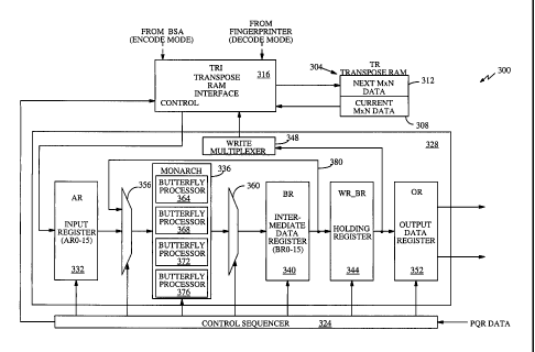
a 2-D DCT
is performed on the four DC coefficients. This 2x2 DCT is called the
differential quad-
tree transform, or DQT, of the four DC coefficients. Next, the DC coefficient
of the
DQT along with the three neighboring DC coefficients with an 8x8 block are
used to
compute the next level DQT. Finally, the DC coefficients of the four 8x8
blocks within a
16x16 block are used to compute the DQT. Thus, in a 16x16 block, there is one
true DC
coefficient and the rest are AC coefficients corresponding to the DCT and DQT.
[0070] Within a frame, each 16x16 block is computed independently.
Accordingly, the
processing algorithm used for a given block may be changed as necessary, as
determined
by the PQR.
[0071] FIG. 3 is a block diagram illustrating computation of the DCT/DQT
and the
1DQT/IDCT of a block of encoded data 300. In encode mode, as illustrated in
FIG. 3, the
encoded data is initially in the pixel domain. As the encoded data is
processed through
intermediate steps, the encoded data is transformed into the frequency domain.
In decode
mode, the encoded data is initially in the frequency domain. As the encoded
data is
CA 02446874 2003-11-07
WO 02/093359 PCT/US02/15916
14
processed through intermediate steps, the encoded data is transformed into the
pixel
domain.
[0072] Referring to FIG. 3, at least one MxN block of encoded data is
stored in a
transpose RAM 304. The transpose RAM 304 may contain one or more blocks of MxN
data. In an embodiment with two blocks of encoded data, one is configured to
contain a
current MxN block of data 308, and the other configure to contain a next block
of MxN
data 312. The blocks of data 308 and 312 are transferred to transpose RAM 304
from the
block size assignment 208 as illustrated in FIG. 2a (in encode mode) or the
fingerprinter
220 as illustrated in FIG. 2b (in decode mode). In an embodiment, the
transpose RAM
304 may be a dual port RAM, such that a transpose RAM interface 316 processes
the
current block of data 308 and receives the next block of data from the
fingerprinter 220.
The transpose RAM interface 316 controls timing and may have buffered memory
to
allow blocks of data to be read from and written to the transpose RAM 304. In
an
embodiment, the transpose RAM 304 and transpose RAM interface 316 may be
responsive to one or more control signals from a control sequencer 324.
[0073] Encoded data enters a data processor 328 from transpose RAM 304 (or
through
the transpose RAM interface 316) into one or more input registers 332. In an
embodiment, there are 16 input registers 332. In an embodiment, the data
processor 328
first processes column data, followed by row data, as illustrated in FIG. 1.
The data
processor 328 may alternatively process the rows followed by the columns,
however, the
following description assumes that column data is processed prior to row data.
The input
register 332 comprises of a single column encoded data of the 16x16 block. The
data
processor 328 computes the transform by performing mathematical operations on
the
encoded data, column by column, and writes the data back into the transpose
RAM 304.
After the columns of data are processed, the data processor 328 processes each
row of
encoded data. After each row of encoded data is processed, the data processor
328
outputs the data through an output register 352.
[0074] In an embodiment, the block of data is a 16x16 block of encoded
data, although it
is contemplated that any size block of data may be used, such as 32x32, 8x8,
4x4, or 2x2,
or combinations thereof. Accordingly, as the data processor 328 is processing
a block of
data from the transpose RAM 304 (for example, the current MxN block of data
308), the
transpose RAM interface 316 receives the next block of data 312 from the BSA
208
(encode mode) or the fingerprinter 220 (decode mode). When the data processor
328 has
CA 02446874 2003-11-07
WO 02/093359
PCT/US02/15916
completed processing of the current block of data 308, the transpose RAM
interface 316
reads the next block of data 312 from the transpose RAM 304 interface and
loads it into
data processor 328. As such, data from the transpose RAM 304 toggles between
the
current block of data 308 and the next block of data 312 as dictated by the
transpose
RAM interface 316 and the control sequencer 324.
[0075] The data processor 328 comprises input register 332, at least one
butterfly
processor within a monarch butterfly cluster 336 and at least one intermediate
data
register 340. Data processor 328 may also comprise a holding register 344, a
write
mutliplexer 348, and output data register 352. Monarch butterfly cluster 336
may further
comprise a first input multiplexer 356, and intermediate data register 340
further
comprises a second input multiplexer 360. The aforementioned components of
data
processor 328 are preferably controlled by the control sequencer 324.
[0076] In operation, for a given column or row of data, the input register
332 is
configured to receive the encoded data through the transpose RAM interface 316
from
the transpose RAM 304. The control sequencer 324 enables certain addresses of
the
input register to send the data through input multiplexer 356. The data input
is
resequenced as by selection through input multiplexer 356 such that the proper
pairs of
encoded data are selected for mathematical operations. Controlled by the
control
sequencer 324, the input multiplexer 356 passes the data to the monarch
butterfly cluster
336. The monarch butterfly cluster 336 comprises one or more butterfly
processors. In
an embodiment, the monarch butterfly cluster 336 comprises four individual
butterfly
processors 364, 368, 372, and 376, and control sequencer 324 routes encoded
data
through input multiplexer 356 to the appropriate butterfly processor.
[0077] Each individual butterfly processor 364, 368, 372 or 376 is capable
of performing
one-dimensional transforms, such as the DCT, IDCT, DQT and IDQT. A one-
dimensional transform typically involve arithmetic operations, such as simple
adders,
subtractors, or a multiplier. After a portion of a one-dimensional transform
is performed
on a pair of data elements, the resulting output is transferred to the
intermediate data
register 340. Intermediate data register 340 may be responsive to the control
sequencer
324. The control sequencer may be a device such as a state machine, a
microcontroller,
or a programmable processor. In an embodiment in which the intermediate data
register
340 is responsive to the control sequencer 324, selected data elements stored
in the
intermediate data register 340 are fed back to appropriate butterfly processor
using a
CA 02446874 2003-11-07
WO 02/093359 PCT/US02/15916
16
feedback path 380 and through first input multiplexer 356, to be processed
again (i.e.,
another portion of a one-dimensional transform). This feedback loop continues
until all
one-dimensional processing for the encoded data is completed. When the
processing of
the data is completed, the data from the intermediate data register 340 is
written to the
WRBR holding register 344. If the data being processed is column data, the
data is
written from the WRBR holding register 344 through the write multiplexer 348
and
stored back into the transpose RAM 304, so that row processing may begin. The
write
multiplexer 348 is controlled to resequence the processed column data back
into its
original sequence. If the holding register data is row data (and thus, all of
the column
processing is complete), the data is routed to the output register 352. The
control
sequencer 324 may then control output of data from the daisy chain multiplexer
and
output data register 352.
[0078] FIG. 4 illustrates a DCT trellis that may be implemented in encode
mode by the
data path processor 328 of FIG. 3. Similarly, FIG. 5 illustrates an [OCT
trellis that may
be implemented in decode mode by the data path processor 328 of FIG. 3. As
dictated by
the PQR data and/or depending on the type of computation being performed, the
control
sequencer 324 may select different pairs of elements of encoded data to
combine and
performs portions of a one-dimensional transform. For example, in the trellis
of FIG. 4,
eight operations occur in column 404. The operations illustrated are as
follows:
x(0)+x(7), x(1)+x(6), x(3)+x(4), x(2)+x(5), x(0)-x(7), x(1)-x(6), x(3)-x(4)
and x(2)-x(5).
Each of the butterfly processors 364, 368, 372 and 376 (as shown FIG. 3)
handles one of
the four operations in a given clock cycle. Thus, for example, butterfly
processor 364
computes the operation of x(0)+x(7) and x(0)-x(7), butterfly processor 368
computes the
operation of x(1)+x(6) and x(1)-x(6), butterfly processor 372 computes the
operation of
x(3)+x(4) and x(3)-x(4), and butterfly processor 376 computes the operation of
x(2)+x(5)
and x(2)-x(5), all in the same clock cycle. The results of each of these
operations may be
temporarily stored in a pipeline register or in the intermediate data register
340, and then
routed to the input multiplexer 360. Operation of the pipeline register is
described in the
specification with respect to FIG. 9c and 9d.
[0079] Optionally, in the next clock cycle, the remaining four
multiplication operations
are computed using the same four butterfly processors. Accordingly, butterfly
processor
364 computes [x(0)-x(7)] * (1/2C116), butterfly processor 368 computes [x(1)-
x(6)] *
(1/2C316), butterfly processor 372 computes [x(3)-x(4)] * (1/2C716) and
butterfly
CA 02446874 2003-11-07
WO 02/093359 PCT/US02/15916
17
processor 376 computes [x(2)-x(5)] * (1/2C516). The results of these
computations are
temporarily stored in the intermediate data register 340. As computations are
completed,
the encoded data is not in the same sequence that the encoded data was in when
originally input. Accordingly, control sequencer 324 and input multiplexer 356
resequences encoded data, or partially processed encoded data after each feed
back loop,
as necessary.
[0080] In the following clock cycle, computations are processed for
column 408, the
results of which are again stored in the intermediate data register 340 are
fed back
through input multiplexer 360. Again, the fed back encoded data, now partially
processed, is resequenced such that the right portions of encoded data are
routed to the
appropriate butterfly processor.
Accordingly, butterfly processor 364 processes
b(0)+b(2) and b(0)-b(2). Similarly, butterfly processor 368 computes b(1)+b(3)
and b(1)-
b(3), butterfly processor 372 computes b(4)+b(6) and b(4)-b(6)and butterfly
processor
376 computes b(5)+b(7) and b(5)-b(7). The resulting computations are again
stored with
the intermediate data register 340 or a pipeline register, and routed through
the input
multiplexer 360. In the next clock cycle, multiplications are performed by 1/2
C18,
1/2C38, 1/2C18, and 1/2C38, in the same manner as described with respect to
column 404.
Thus, butterfly processor 364 computes b(0)-b(2) * 1/2 C18, butterfly
processor 368
computes b(1)-b(3) * 1/2 C38, butterfly processor 372 computes b(4)-b(6) * 1/2
C18,
butterfly processor 376 computes b(5)-b(7) * 1/2 C38.
[0081] In the next clock cycle, computations are processed for column
412 for values in
the d(0) through d(7) positions are computed, the results of which are again
stored in the
intermediate data register 340 and are fed back into input multiplexer 360.
Accordingly,
each butterfly processor computes each stage of each input, such that
butterfly processor
364 computes the operation of d(0)+d(1) and d(0)-d(1), butterfly processor 368
computes
the operation of d(2)+d(3) and d(2)-d(3), butterfly processor 372 computes the
operation
of d(4)+d(5) and d(4)-d(5), and butterfly processor 376 computes the operation
of
d(6)+d(7) and d(6)-d(7), all in the same clock cycle. In the following clock
cycle,
multiplications by 1/2 C14 are computed in the same manner as described with
respect to
columns 404 and 408.
[0082] Column 416 illustrates the next set of mathematical operations
computed by the
butterfly processors in the next clock cycle. As shown in the example of FIG.
4 in
column 416, only two operations are needed during this clock cycle: namely,
the sum of
CA 02446874 2003-11-07
WO 02/093359
PCT/US02/15916
18
the f(2) and f(3) components, and the sum of the f(6) and f(7) components.
Accordingly,
butterfly processor 364 computes f(2)+f(3), and butterfly processor 368
computes f(6) +
f(7).
[0083] In the following clock cycle, the computations expressed in column
420 are
processed. As such, values for h(4), h(5) and h(6) are computed. Accordingly,
butterfly
processor 364 computes h(4)+h(6), butterfly processor 368 computes h(5)+h(8),
and
butterfly processor 372 computes h(5)+h(6).
[0084] As readily observable, FIG. 5 illustrates an EDCT trellis that
operates in a similar
manner, but an opposite sequence than the trellis described with respect to
FIG. 4. The
IDCT trellis is utilized in the decode process, as opposed to the DCT trellis
which
operates in the encode process. The butterfly processors 364, 368, 372 and 376
operate
in the same manner as described with respect to FIG. 4, taking advantage of
efficiencies
in parallel processing. Both in the encode and decode process, a significant
advantage of
an embodiment is the reuse of the same hardware for each stage of the trellis.
Accordingly, the hardware is used for the computations illustrated in column
504 is the
same as the hardware used for computations of columns =508, 512, 516 and 520.
Similarly, the hardware used for the computations illustrated in column 404 is
the same
as the hardware used for computations of columns 408, 412, 416 and 420.
[0085] Once the final results representing the end of the trellis in FIG.
4 are computed,
the data is transferred from the intermediate data register 340 to the holding
register 344.
The holding register 344 and output data register 352 are controlled by
control sequencer
324. If data is column data, the data is transferred to the write multiplexer
348 and stored
back into the transpose RAM 304. Again, the encoded data is resequenced to
reflect the
original sequence of the encoded data. If the data is row data, all
computations are
therefore completed, and the data is transferred from the holding register 344
to the
output data register 352.
[0086] FIG. 6 illustrates an example of a single butterfly processor with
one or more
input and output multiplexers 600. In an embodiment, data output from one or
more
intermediate data registers 340 (see FIG. 3) are coupled to an input portal of
input
multiplexer 604. In an embodiment, the data output from each of the
intermediate data
registers 340 is input into the butterfly processor to a first multiplexer 608
and a second
multiplexer 612. Data output from the input AR register 332 (see FIG. 3) is
also
transferred through the input multiplexer 604. Specifically, the output of AR
register
CA 02446874 2003-11-07
WO 02/093359 PCT/US02/15916
19
AR(0) and AR(8) are coupled to the input of multiplexer 616, and the outputs
of AR(1),
AR(8), AR(9) and AR(15) are coupled to the input of multiplexer 620.
Multiplexers 624
and 628 select either the signal coming from the AR or the BR register as
dictated by the
control sequencer 324 (illustrated in FIG. 3). Accordingly, multiplexer 624
selects either
the data from multiplexer 608 or 616, and multiplexer 628 selects either the
data from
multiplexer 620 or multiplexer 612. The outputs of the multiplexers 624 and
628 are
thus coupled to the input of the individual butterfly processor 632. Butterfly
processor
632 computes a stage of the DCT/IDCT/DQT/IDQT transform, as described with
respect
to FIGs. 3, 4 and 5. The two outputs of the butterfly processor 632, outputs
636 and 638,
are each coupled to the input of each intermediate data multiplexers 642 and
646. Data is
then selected from the multiplexers 642 and 646 to a bank of intermediate
registers 650.
In an embodiment, there are sixteen such intermediate multiplexers and data
registers.
[0087] FIG. 7 illustrates a block diagram of a write multiplexer. As
illustrated in FIG. 3,
the even outputs of the intermediate data register 340 are input into a
multiplexer 704,
and the odd outputs of the intermediate data register 340 are input into a
multiplexer 708.
The data in each of the intermediate registers are resequenced by multiplexers
704, 708,
712 and 716 as controlled by the control sequencer 324 illustrated in FIG. 3,
and stored
in 17-bit registers 720 and 724, respectively. The resequenced data is then
stored in the
transpose RAM 304.
[0088] FIG. 8 illustrates operation of each butterfly processor 800. In an
embodiment,
four butterfly processors are implemented. However, it is contemplated that
any number
of butterfly processors may be implemented, subject to timing and size
constraints. Data
enters the butterfly through inputs 804 and 808. In an embodiment, input 804
sometimes
represents the DC value, and passes through a truncator 812. The truncator 812
is
responsible for the 1/N function, as described with respect to the two-
dimensional DCT
equation infra. The DC value of input 804 is seventeen bits - a single sign
bit plus
sixteen integer bits. The truncator 812 truncates n bits from the DC value
input data to
create a truncated DC value 816, where n is four bits if the data being
processed is a
16x16 block, n is three bits if the data being processed is a 8x8 block, n is
two bits if the
data being processed is a 4x4 block, and n is one bit if the data being
processed is a 2x2
block. If the input is an AC value, truncator 812 is bypassed and routed to a
first selector
814. First selector 814 then selects either the truncated DC value 816 or the
AC value
CA 02446874 2003-11-07
WO 02/093359 PCT/US02/15916
from input A 804. In this embodiment, no fractional bits are used, although it
is
. contemplated that fractional bits may be used.
[0089] The output of first selector 816 is routed to a delay 820 and a
second selector 824.
When the output of selector value 816 is routed to delay 820, the truncated DC
value is
may be held for a clock cycle before being routed to second selector 824. In
an
embodiment, delay 820 is a register. Selection of data in second selector 824
is a
function of the type of mathematical operation that is to be performed on the
data. A
control word 826, preferably routed from the control sequencer, triggers
second selector
824. As illustrated throughout FIG. 8, control word 826 provides control for a
number of
components. Again depending upon the type of mathematical operation to be
performed,
the data then passes to an adder 832 or a subtractor 836. A third selector 828
also
receives the delayed output value from the delay 820, along with input 808.
Again,
selection of data in third selector 828 is a function of the type of
mathematical operation
that is to be performed on the data.
[0090] As the data is either added or subtracted, the data is then passed
to either a fourth
selector 840 or a fifth selector 844 for output from the butterfly processor
800. Input 804
is also passed to fourth selector 840, and input 808 is passed to fifth
selector 844. In
encode mode, the data may also be routed to sixth selector 848. In an
embodiment, in
encode mode, data is routed through an encode delay 852 before being routed to
the sixth
selector 848.
[0091] The second input, input 808, passes through the third selector 828
and the sixth
selector 848. If input 808 is selected by sixth selector 848, the data is
routed to a
multiplier 856, where input 808 is multiplied by a scalar 860. The
multiplication process
with scalar 860 scales the data to produce a scaled output 864. In an
embodiment, the
scalar 860 is selected based on B.G. Lee's algorithm. In an embodiment, the
scaled
output 864 is then routed to a formatter 868. The formatter 868 rounds and
saturates the
data from a twenty-four bit format, a sign bit, sixteen integer bits and seven
fractional bit,
to a seventeen bit format. Thus, the formatted scaled output 872 is seventeen
bits as
opposed to twenty bits in length. Treatment of the data in this manner allows
precision
to be maintained when making calculations, but using fewer bits to represent
the same
data, which in turn saves hardware space. The formatted scaled output 872 is
routed
through a delay 876 to third selector 828 and fifth selector 844, for further
processing.
CA 02446874 2003-11-07
WO 02/093359 PCT/US02/15916
21
[0092] FIGs. 9a-9f illustrate various mathematical operations capable of
being
performed by each butterfly processor. FIG. 9a illustrates a NO operation that
may be
performed by the butterfly processor 900. Given two inputs, input A (902) and
input B
(904), each input is simply passed through to output C (906) and output D
(908).
Accordingly, in a NO operation, C=A and D=B.
[0093] FIG. 9b illustrates an accumulate operation performed by the
butterfly processor
910. Given two inputs, input A (912) and input B (914), output C (916)
represents the
sum of A+B. Input A (912) and input B (914) are combined by an adder 913.
Output D
(918) represents a pass through of input B (914). Accordingly, in an
accumulate
operation, C=A+B and D=B. =
[0094] FIG. 9c illustrates a butterfly DCT operation performed by the
butterfly processor
920. Given two inputs, input A (922) and input B (924), output C (926)
represents the
sum of input A (922) and input B (924), such that C=A+B. Input 922 and input
924 are
combined by an adder 923. Output D (928) represents a subtracter of input A
(922) and
B (924) and multiplied by coefficient CF (930), such that the D=CF x (A-B).
Input 924
is subtracted from input 922 by a subtractor 925, and then multiplied by a
multiplier
927. Optionally, pipeline registers 932 and 934 may be used to temporarily
store the
intermediate product until the next clock cycle.
[0095] FIG. 9d illustrates a butterfly IDCT operation performed by the
butterfly
processor 936. Given two inputs, input A (938) and input B (940), the output C
(942)
represents the sum of input A (938) and input B (940) multiplied by a
coefficient CF
(943), such that the output C=A+(B x CF). Input B (940) is multiplied by
coefficient CF
(943) by multiplier 945, and then added to input A (938) by adder 947.
Similarly, output
D (944) represents the difference of input A (938) and input B (940)
multiplied by a
coefficient CF (943), such that D=A-(B x CF). Input B (940) is multiplied by
coefficient
CF (943) by multiplier 945, and then subtracted from input A (938) by
subtractor 949.
Optionally, pipeline registers 946 and 948 may store intermediate products to
be
computed in the next clock cycle.
[0096] FIG. 9e illustrates an accumulate register operation performed by
the butterfly
processor 950. Given two inputs, input A (952) and input AREG (954), output C
(956)
represents the sum of input A and AREG such that C=A+AREG. As opposed to an
input
value, AREG may also be a value stored from a previous clock cycle in a
register 951.
Input A (952) is added to AREG (954) by adder 953.
CA 02446874 2003-11-07
WO 02/093359
PCT/US02/15916
22
[0097] FIG. 9f represents a DQT/IDQT operation performed by the butterfly
processor
958. Given two inputs, input A (960) and input B (962), output C (964)
represents the
sum of inputs A and B, such that C=A+B. Similarly, output D (966) represents
the
difference of inputs A and B, such that D=A-B. Input A (960) and input B (962)
are
combined by an adder 963. Input B (962) is subtracted from input A (960) by a
subtractor 965.
[0098] The process of calculating a transform of image data 1000 is
illustrated in
FIG. 10, and may be implemented in a structure as described with respect to
FIG. 3. The
process is easily configured for frequency domain techniques such as the DCT,
IDCT,
DQT and 1DQT. A column or row of data initially resides in a transpose RAM
1004 and
is transferred into a holding register 1008 in the butterfly processor.
Individual data
elements of the block of data are selected to be combined 1012, and a
mathematical
operation to be performed on the individual data elements is selected 1016.
Mathematical operations that may be performed are described with respect to
FIG. 9a-9f,
and include no operation 1020, an accumulate 1024, a DCT butterfly 1028, an
DCT
butterfly 1032, an accumulate register 1036 and a DQT/IDQT butterfly 1040. The
results
of the mathematical operation are temporarily stored 1044. A feedback decision
1048 is
then made based on whether further mathematical operations are needed. In an
embodiment, the feedback decision is controlled by the control sequencer, as
described
with respect to FIG. 3. If the data is fed back 1052, the data is fed back to
the holding
register 1008, and the process is repeated. If the data is not fed back 1056,
the data is
transferred to an output holding register 1060. Another decision 1064 is made
as to
whether additional mathematical operations are needed for the column or row of
data. If
so (1068), the column or row of data is transferred to a holder 1072 and then
written back
into the transpose RAM 1004. If not (1076), the block of data is transferred
to output
data registers 1080.
[0099] As examples, the various illustrative logical blocks, flowcharts,
and steps
described in connection with the embodiments disclosed herein may be
implemented or
performed in hardware or software with an application-specific integrated
circuit (ASIC),
a programmable logic device, discrete gate or transistor logic, discrete
hardware
components, such as, e.g., registers and 1411-0, a processor executing a set
of firmware
instructions, any conventional programmable software and a processor, or any
combination thereof. The processor may advantageously be a microprocessor, but
in the
CA 02446874 2003-11-07
WO 02/093359 PCT/US02/15916
23
alternative, the processor may be any conventional processor, controller,
microcontroller,
or state machine. The software could reside in RAM memory, flash memory, ROM
memory, registers, hard disk, a removable disk, a CD-ROM, a DVD-ROM or any
other
form of storage medium known in the art.
[0100] The previous description of the preferred embodiments is provided
to enable any
person skilled in the art to make or use the present invention. The various
modifications
to these embodiments will be readily apparent to those skilled in the art, and
the generic
principles defined herein may be applied to other embodiments without the use
of the
inventive faculty. Thus, the present invention is not intended to be limited
to the
embodiments shown herein but is to be accorded the widest scope consistent
with the
principles and novel features disclosed herein.