Note: Descriptions are shown in the official language in which they were submitted.
CA 02447176 2003-10-28
German Zsatent Application No.10310134.9
tJFTrC~I,~ SIG A~ COUPLIrTG
gIELD OE 'f"H'E IiWEI~TTZON
The present invention concerns an optical signal coupling for two vehicles
coupled with one another, especially rail vehicles coupled with one another,
with a
first coupling part carried by one of the vehicles and a second coupling pert
carried
by the other of the vehicles, betweezt which parts optical signals axe
transmitted. ~'ha
iz~~rention further concerns a conductive coupling for rail vehicles, which
coupling
contains at least one of such signal couplings.
EACKGItOUND O~ THE ~.WE1~TTI(,~N
In vehicle technology four signal, and, data transmission, light conductors
sire
becoming used in increasing numbers which, in contrast to a customary
electrical
signal conductors, provide substantial advantages. Among these advantages are
their larger transmission bandwidths and their similarly small susceptibility
in
respect to electromagnetic disturbance fields. Optical signal couplings of the
above
mentioned kind are necessary if signals are to be transmitted not only within
a
vehicle but also between two vehicles coupled with. one another, such as for
example
the cars of a vehicle train.
An optical signal coupling of the above mentioned kind is for example known
from DE 28 54 962 C2, in which an intermediate buffer coupling for rail
ve~i,rles is
described. A conductive co~xpling belongs to the intermediate buffer coupling
which
among other things serves to transmit impulses for the control of the bralang
and
driv-ixrg currents in a train of vehicles from one vehicle to tile other. The
conductive
coupling consists of two contact carriers each of which is carried by a
respective oae
of the wagons and in which along with a plurality of electrical contacts a
light
conductor is as well arranged. Of the two light conductors at least one is
elastically
biased. so that the two light conductors axe pressed against one another
vi~i,th fiheir
end faces wrhen. the contact carriers upon the coupling of the vehicles axe
moved
1
CA 02447176 2003-10-28
against one another. Through these pressed Together light conducEEors optical
sig~tals
can be transmitted from one vehicle to the other.
Tn the case of such an optical signal, coupling there however appear
significant
transmission failures. A reason for this axes in that the optical signals are
heavily
attenuated in their transmission from. one light conductor to the other, both
because
of a dislocating movement as well as because of a tilting of the optical axes
of the two
Ii,ght conductors relative to one ax<other, ~vrhich leads to a falsification
of, the optical
signals. Cane such dislocating moment or such a upping of the optical axes can
however hardly be avoided in the case of vehicles which are coupled with one
another, since the two coupling parts are notrigidly connected wvi.th one
another and
are relatively heavily mechanically stressed. Further reasons for an
unreliable signal
txansinission lie in the sensitivity of such signal couplings to abrasion and
contatxtiination which, in view of the relatively rough conditions encountered
in the
use of vehicles, are likewise unavoidable.
To drc~unvent these problems an optical signal coupling is proposed in DE 29
22 93? C2 in which the light conductors are not pushed together at there end
surfaces, and instead the light is transmittedwith the help of lens pieces
through the
air from one light conductcar to the other. Such a signal eoupiing is however
relatively complicated and expensive and cannot offer the reliability which
was
expected of it.
In consideration of the above mentioned difficulties recently in DE100 52 020
AX it has been proposed; in the case of applications under rough conditions,
to do
away entirely with a customary optical coupling of light conductors and
instead of
this to first concert the optical signals conducted in a first light conductor
into
electrical signals, to transmit these signals over cv,stornary elecfir;.c
couplings, to again
cor<vert the electrical signals into optical signals and to feed those optical
signals into
a second light conductor, llVith this solution, one loses above all the
previously
zz~.entiorted advantages of an optical signal coupling, namely the increased
transmission bandwidth and a lower susceptibility to electromagnetic
disturbing
fieids. Since however in the coupling regions of vehicles typically
accompanying
signals of high current are transmitted and thereby directly produce strong
2
CA 02447176 2003-10-28
electromagnetic disturbing fields, it is not beneficial to replace the optical
signal
coupling by an electric coupling sensitive to the disturbing fields. Moreover,
the
coupling region of vehicles offeis only a limited space fox the signal
coupling, so that
optical signal couplings with their high transmission bandwidth are more
efficsently
used than electrical couplings. .
The present invention has as its object the provision of an optical signal
couplzng which assures a reliabXe transmission of signals between vehicles
coupled
with one another.
S'UMM~4~Y ~F THE TN'iIENTIC)N
This object i5 solved with an optical signal coupling of the previously
mentioned Idnd in that the first coupling Part includes a sendixig de~rice
which
creates the optical signals to be transmitted, and. the second coupling part
includes a
receiving device which detects the optical signals transmitted.
In contrast to customary signal couplings which essentially, with respect to
their nature, represent the passive coupling of two light conductors, the
signal
coupling of the invention has active elements with the help of which the
optical
signals to be trax~.smitted are produced only in the 5igxlal coupling and the
transmitted opfi'tcal signals are detected while still in, the signal
coupling.
Since the optical signals are intended to pass exclusively through the signal
coupling they can be suited to the speci.aI optical characteristics of the
signal
coupling, so that the reliability of the signal transmission. is substantially
increased.
If the signal coupling, for example as a result of contamination, abrasion,
moisture- or
mecharuical inaccuracies, produces a higher attenuation of the transmitted
signals
than expected, the signal Created in the first coupling can be correspondingly
strongly produced and the increased attenuation thereby compensated.
Achxally, because of this compensation possibility a certain optical
athenuation
by the signal coupling is acceptable, which lowers the quali~r requirements
for the
optics of the signal coupling. Thereby nnanufa~g costs can be saved to an
extent
CA 02447176 2003-10-28
which more than equals the expense of the provision of the sending and
receiving
devices.
Zt is even gossl'ble to create optical signals in the ~xst coupling part which
are
so strong that they can already be received by the second coupling part when
the
vehicles indeed stand ,close to one another, but are not yet coupled, so that
the end
faces of the light conducfing elements are not yet engaged with one another. A
signal transmission in the uncoupled condition can for example be useful
during a
coupling procedure in a curve. In this case information about the position of
the ,
wheels relative to the vehicle can be transzxvtted, which gi~res irifozrnation
about the
curvature of the curve and thereb~r helps the positioning of the parts of the
mechanical coupling for the coupling procedure.
!n the transmission of a signal from one vehicle to the other the signal path
iri
the usage of the signal coupling of the invention is constantly divided into
three
sections: a secfiion from a signal source to the first coupling part, a
section from the
second coupling part to the signal goal, and an intermediate section in which
the
signal in the form of the opty.cal signal. produced in the sending device of
the first
coupling-part passes thmugh the signal coupling. Tf the signal arrives at the
goal in
faulty condition, it can be relati~rely easily. detern~ined in which of the
three sections
the source of the. faults lies. For example, control signals can accompany the
optical
signals created ixt the sending devices, by means of which the receiving
device can
determine whether the correct signals have been ixansmit~ed. lbloreover the
signal
can be refined in the sending and receiving devices so as to likewise increase
the
reliability of the signal transmission.
In the case of customary optical signal couplings, the disturbances accumulate
in all three sections. Thereby not only slight transmission errors appear, but
it is also
difficult to determine in which sections of the signal path the origin for the
distczrbances lies, onto determine if perhaps a cornbW .ation of disturbing
sources is
present and not only a single disturbing source as the reason for the encors.
A fadvantage of the signal coupling of the inwent~on lies in that it is
more widely usable than customary ones. 'Whereas cusf~omary optical signal
4
CA 02447176 2003-10-28
couplings, as mentioned, essentially serve to connect two light conductors
provided
in the coupled v~ehictes, with tk~e signal coupling of the irwention sigx~als
of general
kind can be transmitted, that is independently of whether they are present in
dte
individual vehicles as optical, electric, hydraulic or pneumatic signals. For
in each
case the signal (electric, optic, hydrasdic ox pneumatic) present in a vehicle
is
converted in the sending device of the fist coupling part into an optti..cal
signal
ixrtended espedally for passing through the optical signal co~xpling, which
i.s
detected by the receiving device of the second coupling part and which is then
reconstructed as the original (electric, optic, hydraulic or pneumatic) signal
and
conducted on to the other ~rehide.
Preferably, the first coupling part includes a microprocessor which controls
the creatiox~ of the signals in the sending device. Additionally or
altenxatively, the
second couplir~g part preferably contains a microprocessor which processes the
signals detected in the receiving device. By the use of microprocessors for
the signal
production and the signal processing the reliability and flexibility of the
optical
signal. coupling can be further increased. JFor with the help of the
microprocessors
the signals can among other things be tested and refined. Moreover, by means
of the
optical coupling signal two vehicles of differing constructional types can be
connected wherein the signals axe processed and/or conducted in different
ways.
The signal can then with the help of the microprocessors be conducted. The
signals
can with the help of the microprocessors already in the signal coupling be
brought
info the forms which are required by the individual vehicle.
In an advantageous development the xnicropirocessor of the first coupling part
is so programmed that it combines several individual signals into multiplexed
signals, and the microprocessor of the second coupling part is so programmed
that
the rilultiplexed signals are divided into several individual signals. In this
case
several different signals can be transmitted by the signal coupling at the
same time
so that additional. signal couplings are spared.
In an advantageous further de~reXopment of the optical signal coupliarlg in
each
of the first and second coupXing parts a fight conducting element is contained
of
which one has a spherical concave end surface and the other a spherical convex
end
CA 02447176 2003-10-28
face with the same radius of curvature, with at least one of the elez~nents
being so,
elastically biased that the light conducting elements are pressed against one
another
with their end faces when the two vehicles are coupled with one another. In
the
coupled condition the convex end face of the one coupling part lies exactly
iz~.atchingly in the concave end face of the other coupling part, and indeed
without
leaving an air gap between the end faces, which air gap would have an
attenulating
effect on the optical signal.
dy way of the pressure force resulting from the biasing of the one or both
light
conducting elements, the convex end surface is pressed into the hollowing of
fhe
conca~re end face so that the two coupling parts are automatically centered
with one
another. Thereby with the signal coupling a xriechanical displacement of the
optical
axes of the light cond~x~g elements is avoided, which in the case of customary
signal couplings leads to an attenuation of the optical signal.
Moreover, the spherical end faees allow a tilting of the optical axes of the
light
conducti~:g elements relative to one another without the end faces being
lifted from
one another. rn the case of such a tilting the spherical convex surface slides
on the
spherical cancave surface, like a socket joint head in a sockef joint socked,
without ,
produang an air gap between the end faces. This is a great advantage in
comparison
to customary signal couplings wzth flat end faces between ~nrhich in the case
of a
tilting of the coupling parts relative to one another without fail an air gap
is foamed,
which leads to a non-permissible attenuation of the transaliitted signal.
The possibilit3r of a small attenuation as a result of a tilting of the
coupling
pazt5 relative,to one another is especially of great significance if the
signal coupling is
used to transmit optical signals between rail vehicles. Although in the case
of
customary signal couplings for rail vehicles it is attempted to guide the
coupling .
parts linearly, that is to prevent a tilting of the coupling relative to one
another, this.
is not achieved reliably in practice because of the high mechanical leads,
which leads
to an excessive attenuation of the transmifted optical sig~tals. With the
described
improved signal coupling t'he prindpal of a linear guiding can be eniirel~r
avoided,
because even a relatively large tilting of the coupling parts relative to one
another
6
CA 02447176 2003-10-28 ------
leads to a tolerable attenuation of the signals. The improved signa). coupling
is
therefore.fo a given degree "bendable."
Preferably, the Iight conducting elements of the improved signal coupling
each include a light opaque sleeve and a transparent core received in the
sleeve. Zf
the coupling parts are coupled, the light opaque sleeves form a Iight tunnel
sl~,elded
from daylight. Thereby even in the case of a tilting of the light conduet3ng
elements
relative to one another no daylight can. fall into the transparent core,
assuming that
the wall thicknesses of the sleeves ia~ the region of the eyed faces are not
too small.,
Preferably these wall thicknesses have values which are at least x / to and
preferably
at least 1 J 5 of the radius of curvature of the end surfaces.
In a preferred further development the light opaque sleeves are electrically
conducting and upon the pressing together of the end faces of the light
conducting
eleiments_ of the two coupling parts form an electd.cal contact between the
associated
sleeves through which elecfiric signals are transmittable from one coupling
part to
the other coupling part. Thereby a second, independent channel for the
transmission
of signals is made which further increases the reliability of the optical
signal
coupling.
When the light conducting elements each comprise a light opaque sleeve and
a transparent core, each associated spherical end face in the normal case has
one
sectiozi formed by the sleeve and another section formed by the transparent
core.
When. the core and the sleeve for example have a cylindrical form the portion
of the
end ~ace formed by the core has the shape of a ball segment, which in the
nornxal
case is smoathly continued by an annular secfiion formed by the sleeve.
In the above-mentioned further development) in which the electric signal is
transmitted through the sleeves, the section of the end face formed by the
sleeve is
preferably plated with hard gold to obtain a corrosion resisting contact.
To achieve a good electric contact between the sleeves, it is advantageous if
the sleeve is allowed to extend somewhat beyond the transparent care. In this
case
th.e end surfaces, as the surfaces by which the light conducting elements
engage one
CA 02447176 2003-10-28
another, differ from. the above described normal, case in that they are only
formed by .
the spherical3.y formed sleeve end which has the shape of an annular
spherical:
segment. Such a spherit:al section for this purpose of this description is
also referred
to as a "spherical surface." Accardingly the spherically shaped slee~re end is
to be
taken as a speaal case of the above nnenfiioned °'spheri.cal end
surface."
T'referably, at least a portion of the signal which is transmitted as an
optical
signal between the coupling parts is additionauy transmitted as an electrical
signal
thro~xgh the sleeves of the two coupling parts. In the event the transmission
of the
optical signal is disturbed or should entirely fail one has this otherv~ise
redundant
electrical signal in reserve. This doubled transmission in different ~nrays is
of a great
importance in the case of safety relevant signals (for example braking signals
in a
connected train of vehicles), for which ~ fault containing or inoarriplete
signal
fransrnissi.on must definitely be avoided.
Preferably, the first and/or second co~ipling part of the signal coupling has
a
housing on one axial end of which xs formed a sleeve like section in which the
light
conducting element is slidably supported and is elastically biased in a
direction
toward this one axial end, and at the other end of which a connecting pin is
formed,
which is designed for installation in a contact carrier.
When the sleeves of the light coiLducting elements are electrically
cox~ducfang,
there preferably exists between the sleeves of the light conducting elements
and the
sleeve Iike section of the housing o~ one of f~ose~aceompanyixvg parts an
electrie
sliding contact through which electric signals are transmittable. Then this
housing
can. be used for tlhe receiving and further conducting of the electric
signals.
The connecting pin preferably comprises two sections insutated from one
another o~ which one i,s connected with gmurtd potential and the other with an
electric signal conductor, when the eonxtecting pixy is installed in the
contact carrier.
apticai signal couplings for vehicles usually are integrated izzto special
conductor couplings, the halves of which have a small mechanical play. Since
the
described signal coupling however is much less sensitive to a displacement of
the
8
CA 02447176 2003-10-28
coupling parts rnrnlative to each other than is a normal coupling, a special
canductox
coupling for it is not absolutely' necessary. Instead, the coupling parts can
also be
arranged directly into the coupling heads of a mechanical couplixtg. The play
which
typically appears between the coupling heads can be accoaunodated by the
illustxated optical signal coupling wifhvut that play influenang its
functioning.
The invention further concerns a conductive coupling for the connecting of
conductoz~s of two rail vehicles couplable tnrith one another, with two
contact carriers
each a~ which is attached to a respective one of the rail vehicles, and wvi.th
at least one
signal coupling part with a sending device being arranged in one contact
carxxer and
with at least one signal. coupling part with. a r~eceivi,ng device being
arranged in. the
other contact carrier, which coupling parts together form an optical signal
coupling
of one of the above described kinds.
Preferably in this case in each contact carrier is arranged both a signal
coupling part with a sending device and a signal eoupling part with a
receiving
device which together form twc~ opfiical signal couplings of dne above
described kind.
Thereby from both the sides of the conductive coupling opfical signals cari be
sent to
the other side. In this case preferably the sending and receiving devices of
the
coupling parEs of each contact carrier are connected with a common
zni.croprocessor
which controls the creation of the signals in the sending device and processes
the
signals detected in the receiving device.
BRIEF DESCRIPTION' ~F THE DRAWINGS
Further features and advantages of the invention will be apparent fraxx~. the
follovrring descripfiion in which the signal coupling is explained in .more
detail. by
way of arc exemplary embodiment. The drawings are:
Fig. l A sectional view of a first coupling part of a signal coupling in
exploded
illustration (upper) and in assembled condition (lower),
Fig. 2 A sectional view of a second coupling part of a signal coupling in
exploded
9
CA 02447176 2003-10-28 -.,
illustration supper) and in assembled condition (lower),
'Fig. 3 A sectional view of the coupling parts of Figs.1 and 2 in coupled
coindition,,
Fig. 4 The coupled coupling laax~ts of Fig, 3; the spaax~g of which in fine
direction
of the optical axis has been shortened;
Fig. 5 The coupled coupling parts of Fig. 3, the optical axes of which have
been
tilted relative to one another,
Fig. 6 A functional sketch of a sending device of the first coupling part,
Fig, 7 A functional sketch of a receiving device of the secand coupling part,
and
Fig. 8 A sectional view of a portion of a cond~xctor coupling for rail
vehicles
with two contact carriers, in each of which a coupling part of the signal.
coupling is used.
DETAILED DESCItTPTION OF TkIE 1'REFEIZRED EM~ODrMENT
Shown in Fig.1 is a longitudinal sectional ~cri.ew of the first coupling part
10 of
a signal coupling according to a development of the present invention in
exploded
illustration (upper) and in assembled condition (lower). In Fig. 2 is showtL a
longitudinal sectional illustration of the second coupling part 12 of the same
signal
coupling in exploded illustration (uppex) and in assembled condition (lowex).
Since
the first and the second coupling parts 10 and 12 are identical in many
features, they
will be described in common m the following with similar parts being
i.ridi.cated by
the same reference characters.
The coupling parts 10 and 12 each. have a housing 14 ,wiith. a sleeve like
section
I6 in wrhich a light conducting elemeant 1g is a~ci.ally slidably supported.
The light
conducting element 18 can be pressed into the sleeve-likre section 16 of the
associated
housing 14 against the biasing force of a spring 20. In place of the spring
20, fhe light
1U
CA 02447176 2003-10-28 -_....
conducting element 18 can also be biased by a gas captured in the sleeve-like
section
16. Each light conducting element 18 includes a light opaque sleeve 22 and a
transparent core 24 received in the sleeve 22.
The light conducting element T,8 of the first coupling part has a spherically
concave arid surface 26 facing away from the sleeve like housing section 16
(Fig.1),
and the light conducting element 18 of the second coupling part 12 has a
spherically
convex end surface 26' (Fig. 2), the radius of curvature of which. corresponds
to that
of the spherically concave end surface 26. The spherically concave end surface
26
and the sp~.erically convex end surface 26' are formed not only in the
transparent
core 24 but are also contixtued in the axial ends of the associated sleeves 22
of the
light conducting elements 18.
The spherical end surfaces 26 and 26' of the first and second Coupling parts
10
and Z2 have therefore a portion 26a and 26'a formed by the transpare~c~.t core
24 and a
portion 26b and 26'b formed. by the sleeve 22. The secfiions 26b and 26'h are
thereby
annularly shaped spherical segments. biowe~rer, in the following description
such a
spherical section is referred to as a "spherical surface."
Guide grooves 27 axe formed in the sleeves 22, which guide grooves receive
guide pins 28. The shifting movement of the light conducting element 18 is
thereby
limited by one of the ends of the guide groove 27 engaging a guide pin 28.
The inner space of the sleeve-Like housing section 16 is nnade up of two
cylindz ical sections, one being an inwardly lying section 30 and the other
beixig a
more outwardly lying section 32, the diameter of which is larger than that of
fhe
inwardly lying section 30. Between the cylindrical inner space sections 30 and
32 is a
shoulder 34 fo~ned in the housing inner wall. In the outer inner space section
32 are
located the light conducting element 18 and the spring 20, which spring at one
end
engages the light conducting element 18 and with its other end engages a metal
ring
36 which in turn lies on the shoulder 34.
Ian the inner inner space section 30 in the case of the first coupling part 10
is a
sending device 38 (Fig.1~ and in the case of the second coupling part is a
receiving
11
CA 02447176 2003-10-28
device of 40 dig. 2). Each of fihe sending device 38 and the receiving device
40 has a
ground connection 42 which is soldered to the sleeve-Iike section 16 of the
housing
14, and each has a signal terminal 44.
The housing 14 has at its end facing away from. the light conducting element
1S a hollow connecting pin 46 with a ground connector section 48, a signal
connector
section 50, and lying between them an insulating piece 52 which elecixically
isolates
the sections 48 and 50 from one another. The signal connector ~ is guided
through
the hollow space of the connector pin 46 and is soidered with the signal
connector
piece 50. The ixiner inner space section 30 and the hollow space of the
connector pin
46 are filled with pottant material illustrated in Figs.1 and 2 by cross
hatching. An
exfiexna3. thread 54 is formed on the ground connector section 48 of the
connector pin
46 b~ means of which the coupling parts 10 and 12 are threadable into, a
ground
potential socket of a contact carrier.
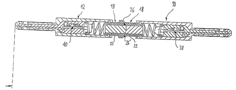
In Fig. 3 the first coupling part 10 and the second Coupling part 12 are shown
in coupled condition. In this condition, the end faces 26 and 26' of the
associated
Light conductor elements 18 are pressed onto one another so that the optical
signals
which are fed into the transparent core 24 of the light conducting element 18
of the
first coupling part 10 by the sending device 38 are transmitted through the
end faces
26 and 26' into the transparent core 22 of the light conducting element 18 of
the
second coupling part 1,2 and become detected by the receiving device 4U.
Further,
the light opaque sleeves 22 of the light conducting elements 28 form a light
tunnel,
shielded from daylight,, which connects the sendiing device 38 and the
receiving
device of 40.
Sinr~e the two light conducting elements '18 are each slidable in the housing
14
of the associated coupling part 10 or 1.2 the coupling parfis can be moved
somewhat
away from and toward one another without disturbing fine functioning of the
signal
coupling. In Pig. 4, ~ar example, the coupling parts 10 and 1.2 of Fig. 3 have
been
moved somewhat toward one another wifhout that haring changed the positiozts
of
the light conducting elements 18 to one another, so that the light
transmission
remains undisturbed. The nLJ.ustrated signal. coupling therefore assures a c
tolerance in the relative arrangement of the two coupling parts 10 and ~2 in
the
12
CA 02447176 2003-10-28
coupling direction, that is along the optical axes of the light conducting
elements 18,
which optical. axes are formed by the middle axes of the lig~tt conducting
elements.
I8. Further, the spring pressure biased end Faces 26 and 26' prevent
displacement of
the optical axes of the light conducting elements 18 against one her, that is
they
help to orient the coupling parts to one another and to maintain the ariented
positions.
In Fig. 5, the two coupling parts 2Q and 12 are likewise shown in ca~xpled
conditio~x. Differently than in Figs: 3 and 4, in this case the coupling parts
1,0 and x2
are not aligned with each other, 'but instead are tilted relative to ozte
another. That
means that the optical axes of the light conducting elements 18, each of which
coincides with the symmetry axis of the associated transparent core 2~, stand
at an
angle to one another. Because of their spherical shape, the end surfaces 26
and 26'
nevertheless lie without gap on one another, so that the attenuation of the
light upon
passage through the end surfaces 26 and 26' is held within limit. The signal
coupling
is therefore bendable to a certain degree, without such bending xnfluericix~.g
its
fi~.nction. 'this is a Large advantage in comparison to customarily used flat
end faces
which upon surh a bending become lifted from one another so that the light
transmission from one coupling part to the otheF becomes, heavily attenuated.
In Fig. 5, the signal coupling is shown in its maximally bent condition, in
which the coupling parts are bent about lh° relative to one another. In
the case of a
further bending daylight would enter the light tunnel and falsify the optical
signal.
The limiting angle at which daylight penetrates into the Light tunnel depends
on the
relationship of the wall fihicknesses of the light opaque sleeves in the
region of the
end faces 26 and 26' to the z~adius of curvature of the end faces 26 and 26'.
In the
illustrated exaruple, the wall thickness of the light opaque sleeve 22 of the
first
coupling part 10 in the area of the end face 26 is smaller than that of the
light opaque
sleEVe 22 of the second coupling 1.2y and is therefore dete~cnvnati~re of the
value of the
limiting angle. It measw~es about 1 / 5 of the radius of curvature of the
spherical end
surfaces 26 and 26'.
As is to be taken from Figs. 3 to 5, the twro coupling parts 10 and 12 engage
one another with their spherical end surface sections 26b and 26'b formed by
the
I3
CA 02447176 2003-10-28 ..._...___._.. _._____.._._______
sleeves ?.~. Therefore electrical signals can be fransmitted additionally
thxough the
two sleeves 22 betrween the two coupling parts Io and 12 insofar as these
sleeves are
made to be electrically conductix~.g. The end surface seeti.ons ebb and 26'b
are then
preferably plated with hard gold.
By way of the additional transmission possibility for electrical signals the
reliability of the signal transmission can be further increased. Especially as
a safety
reserEre, it is advisable to transmit the optical signalss or the mast
important portion
of them, additionally as "redundant" electrical signals thxough the sleeves
22. To
deliver the electrical signals to the sleeves 22 and to again conduct them
away from
the sleeves, in a modification of the coupling (not shown in the figures) the
signals .
can be conducted through the housing 14, which in this case differs from that
illustrated in Figs. Z to 5 by not being connected in ground. Between the
sleeve-like
housing section T6 and the sleeves 22 a sliding contact (not shown) can then
be used.
Fig. 6 shows a functional sketch of the sending device SS. As is to be taken
from. this, an input voltage Vin is applied between the ground connection ~2
and the
signal connection 44 through a scaling resistor 56 and is applied through a
high pass
filtex, consisting of a capacitor 58 and a xesistor of 60, to a light emitting
diode 62,
which emits light corresponding to the applied voltage. The relationship
between
the applied voltage Vin and the radiated power S of the light emitting diode
62 is
schematically represented in the diagram in the right portion of Fig. 6, whose
abscissa indicates tune. and where ordinate gives the input voltage V'm, and
the
radiation power S in undefined units.
Fig. 7 shows functional sketch of the receiving de~rice 40 . The r~ecei~ring
device 40 includes a photodiode 64 which in dependence on the intensity of the
incoming light produces a voltage. This voltage is suitably amplified in a
first circuit
section with the help of an operational amplifier 66, a resistor 68, and a
capacitor 70,
and is inverted with the help of a further operational amplifier 72 to an
output
voltage'Vout. The relation between the received emission poirver S' (which
multiplied by an attenuation factor corresponds to the radiation power emitted
from
the t.ED 62) and the output signal Vout of the receiving device 40 is
schematically
illustrated in the diagram in the right portion. of Fig. 7, the abscissa of
which again
't4
CA 02447176 2003-10-28
shows time and the ordinate of vrrhich shows the received env~sio~t power S'
and the
output voltage Vout in undefined units.
The sending device 38 and the receiving device 4fl are so designed that the
output signal Vaut of the receiving deulc~ 40 despite a possible attenuation
of the
Eransmitted optical signal corresponds to the input voltage Vin. Therefore,
even if
the optical signal transav,tted between the coupling parts 10 and 12 xs
subjected to a
certain attenuation, the effective txansrtutted electric signal Vout is not
attenuated in
respect to the original signal Vin.
The electric input sigma'! Vin can: for example be an eXectrical high
frequet~.cy
signal which iiulside of tyvo vehides is conducted through a co-axial cable
and. only to
suit the signal coupling is converted into an optical signal with the help of
the
sending device 38. The signal coupling with the active elements 38 and 40,
hovtrever,
finds for example other uses if in the ~rehicle optical signals are already
transmitted
through light conductors. These signals are then in the first coupling pant
1.0 fist
converted to an electric signal which is then applied to the sending device
38. The
output sig~i~.ai Vout of the receiving device 40 is then in the second
coupling part
again converted into an optical signal and supplied to a subsequent light
conductor.
Fig. 8 show's in secEional illustration a section of a light coupling for use
in
combination v~ith an automatic rail vehicle coupling. An automatic rail
vehicle
coupling is used if the towed members have to be often coupled and de-coupled.
Then the associated conductive coupling is so designed that its electrical and
optical
contacts are likewise automatically coupled along with the automatic coupling
of the
towed membexs.
The conduciav~e coupling includes two contact carriers ~4 and 76 in which,
along with a row of electrical contacts (nit shov~n) the above-described
coupling
pants 1fl and 1.2 of the signal coupling are also used. The coupling gams at
10 and 12
az~e forwardly threaded into the contact carriers 74 and 76 by means of the
threads 54
of the connector pins 46, whereby the thread 54 is subjected to ground
potential, ,At
the same timer the signal contact section 50 of the first coupling part 10
crnmes into
electrical contact with a schematically illustrated fiyrst signal processing
unit 78 and
~.5
CA 02447176 2003-10-28
the signal. co~ut~ector section 50 of the second coupling part 12 comes into
electric
contact with a schematically illustrated. second signal processing unit 80.
Tt will be understo~ that the coupling paxts 10 and 12 are very easily
installable and rernavable. This provides a big advantage ~,xr compari.san to
customary optical signal couplings whose coupling parts are connected with
light
conductors and ran only be installed or exchanged with great difficulty, and
especially not from the forward ends of the contact carriers 74 and 76.
In the illustrated exemplary ecnbodirnent the first signal, processing unit 78
is
supplied with electric signals over a co-axial cable 82 and optical signals
over a light
conductor $4. The optical signals of the light eonducbor 84 are converted into
electrical signals in a converter unit 86 and together with the electrical
signals o~ the
electrical conductor 82 are delivered to a control unit 88. Tn the control
unit 88 the
two inputted electrical signals are processed into a mu'~tiplexed signal which
is
transmitted to the signal connector 50 of the first coupling part For this the
coxttrol
unit 8$ has a microprocessor (not shown), which iztcludes an industrial T'C or
a so-
calIed field programmable gate array (FPGA). In comparison to customary
microprocessors an FPGA has the advantage that it can process several commands
simultaneously as is required for a genuine mufti-tasking in the involved
circumstances.
The control unit 88 is fmckher connected with a data-conductor 90 over which
further inforrnatian for the signal processing can be delivered. For example,
through
the data conductor 90, it can be signaled that already transmitted signals
have not
been completely received and should be sent again.
The conversion of the electric multiplexed signals into optical signals by the
sending device 38 and their transmission from the first coupling part 10 to
the
second coupling part 12 takes place in the way described above. From the
signal
connector 50 of the second coupling part 1.2, the elec°trieal sigx<aIs
created in the
receiving device 40 reach a confirol unit ~2 of the second sigx~al processing
unit S0. In
the control unit 92 the rn.ultiplexed signals are divided into individual
signals. The
original ingoing signals from the electric conductor 82 are further conducted
by an
16
CA 02447176 2003-10-28
electrical conductor 94. 'The original ix~going signals from. the light
conductor 84 are
converted again into optical signals in a converter unit 96 and are supplied
to a light
conductor 98.
8y means of a further data conductor 100 signals from the control unit 92 can
be further condv.cted, for example fault reports if signal errors have been
received.
The contcoI unit 92 contains likewise an indusfrial PC or an PPG, (not shown).
Tile signal processing units 78 and 80 can also be contained in the housings
14
of the coupling parts IO and 12. Further, the signal processing units 78 and
80 can
each be connected with a ixansmission capable coupling part (sr.mi:lar to the
first
coupling part 10) and a reeeiv~ing capable coupling part (similar to the
second
coupling part 12). They, signals can be transmitted from both sides of the
coupling
to the other side and the signal processing units of 7S and 80 can communicate
with
one another in both dired3ons.
The coupling parts 10 and I1 can above all be not only arranged in special
contact carriers as shown in Pig. 8, but can also be arranged in the coupling
heads of
a mechanical rail vehicle coupling, for example in an automatic inteimedia~e
buffer
coupling (not shown). The above described ia~sensitivi~ of the optical signal
coupling with xespect to mechanieal tolerances makes this arrangement
possible,,
~rhich would not function in the case of a customary vpfiieal signal coupling.
Thereby in many cases a separate conductor coupling can be spared.
17
CA 02447176 2003-10-28
REFERENCE CHARACTER LIST
ZO - first coupling part
12 - second coupling part
1.4 - housing
26 - sleeve-like houtsing section
18 d light conducEing element
20 - spring
22 - light opaque sleeve
24 - txansparent core
26, 26' - spherical end surfaces
2? - gui.de groove
28 - guide pix<
30 - inner inner space section
32 - outer inner space section
34 - shoulder
36 - m.etal Ping
38 - sending unit
40 - receiving unit
42 - ground, connector
44 - signal connector
46 - connector pin
48 - ground connector section
50 - signal connector secfiion.
52 - insulating piece
54 - exter:naX thread
S6 - resistor
58 - capacitor
60 - resistor
62 - 'QED
64 - photo diode
66 - operational amplifier
68 - resistor
70 - capaafor
18
CA 02447176 2003-10-28
~2 - operational amplifier
~4 - contact carix,er
76 - eontact carrier
78 - signal processing u~v,t
80 - signal processing unit
82 - electric signal conductor
84 - light conductor
86 - signal converter
88 - control unit
90 - data conductor
92 - confrol unit
94 - electric signal conductor
96 - signal converter
98 - light conductor
7.00 - data conductor
19