Note: Descriptions are shown in the official language in which they were submitted.
CA 02447177 2003-10-28
German Patent ,Application No. I0310Z48.9
LYGHT Ct7NDUCTOI~COUPLING
FIELD OF THE INVENTION
The present invention concerns a light conductor coupling, especially for the
transmission of optical signals between vehicles a coupled with one another,
with a
first and a second coupling part which are couplable with one another and in
each of
which is contained a light conducting element, of which light conducting
elements at
least one is elastically biased so that the light conductor elements are
pressed against
one another with their end surfaces, when the coupling pants are coupled with
one
another, to permit a transmission of light from one light conducting element
tv the
other.
BACKGROUND OF TIC INVENTION
One such light conductor coupling is for exanl.ple known from DE 28 54 962
C2, in which an intermediate buffer coupling for rail vehicles is described.
~. cable
coupling belongs to the intermediate buffer coupling which among other things
serves to transmit impulses for the control of the bxaking and driving
currents from
one vehicle to the other in a train of vehicles. The cable coupling consists
of t~nro
contact carriers each of which is carried by a respective one of the ~rehicles
and in
which along with a plurality of electrical contacts a light conductor is as
well
arranged. Of the two light conductors at least one is elastically biased so
that the 'two
light conductors are pressed against one another with their end faces when the
contact carriers upon the coupling of the vehicles are moved against on.e
another.
Trough these pressed together light conductors optical signals can be
transmifted
from one vehicle to the other.
From 'DE 198 07 596 C2 a light conducting plug connector of the previously
mentioned type is known in which not only one, but both light conductor
elements
are elastically biased.
1
CA 02447177 2003-10-28
When light conductor couplings of fihe above-mentioned type are used under
rough conditions, such as for example for the transmission of signals between
coupled vehicles, (here however appear many transmission failures. A reason
for
this Lies in that the optical signals are heavily attenuated in their
transmission from
one light conductor element to the other, both because of a dislocating
movement as
well as because of a tilting of the optical axes of the two light conductors
relative to
one another, which leads to a falsification of the optical signals. One such
dislocating
movement or such a Tipping of the optical axes of the light conducting
elesx~.ents can
however hardly be avoided in the case of vehicles which are coupled with one
another, since the two coupling parts are not rigidly connected with one
another and
are relatively heavily mechanically stressed. JFurther reasons for an
unreliable signar
transmission lie in the sensitivity of such light conductor couplings to
abrasion and
contamination which in relatively rough. conditions are likewise unavoidable.
To circumvent these problems an optical signal coupling is proposed in lDE 29
22 937 C2 in which the light conductors are not pushed together at their end
surfaces,
and instead the light is transmitted with the help of lairs pieces through the
air from
one light conductor to the other. Such a signal coupling is however relatively
complicated and expensive and cannot offer tine reliability which was expected
of it.
In consideration of the above mentioned difficulties in DE10D 52 020 A2 it has
been proposed, in the case of applications under rough conditions, to do away
entiz~ely with a customary optical coupling of light conductors and instead of
this to
first convert the optical signals conducted in a first light conductor into
electrical
signals, to transmit these signals over customary electric couplings, to
again. convert
the electrical signals into optical signals and to feed those optical signals
into a
second Iight conductor. With this solution, one loses above all the previously
mentioned advantages of a light conductor coupling, namely the increased
transmission bandwidth and a Iower susceptibility to electromagnetic
disturbing
fields, especially those which always appear if in the immediate
via.nity',high
currents are also transmitted, as for example in cable couplings for rail
vehicles is
often the case.
2
CA 02447177 2003-10-28
The invention has as its basic object the provision of a light conductor
coupling which is of simple construcEion and which permits a disturbance
insensitive signal transmission.
S'tJMMAItY OF THE IhTVEIVTIO1~T
This object is solved by way of a light conductor coupling of the above-
rn.entioned kind in that the end surface of one of the light conductor
elements is
spherically concave and the end surface of the other light conductor eleu~ent
is
formed spherically eonvex with the same radius of curvature.
In the coupled condition the convex end surface of the one coupling part ~,es
exactly fittingly into the convex end surface of the other coupling part, and
indeed
without an air gap between the end surfaces, which air gap would lead to an
attenuation of the optical signals.
By the biasing of the one ox both light conductor elea~.ents, the convex end
surface is pressed into the hollowing of the concave end surface so that the
two
coupling parts are automatically centered with one another. Thereby with ~e
light
conductor coupling of the invention a mechanical displacement of the optical
axes of
the light conducting elements is avoided, which in the case of customary light
conductor couplings likewise leads to an attenuation of the optical signals.
Moreover, the spherical end faces allow a tilting of the optical axes of the
light
conductor elements relative to one another without the end surfaces being
lifted
from one another. In the case of such a tilting the spherical convex surface
slides or_
the spherical rcmcave surface, like a socket joint head in a socket joint
socket, without
produang an air gap between the end faces. This is a great advantage i~.
comparison
to customary light conductor couplings with fiat end faces between which in
the case
of a tilting of the coupling parts relative to one another ~nrithout fail an
air gap is
formed, which leads to a non-permissible attenuation of the transmitted sig
naI.
The possibility of a small attenuation as a result of a tilting of the
couplimg
parts relative to one another is especially of great significance if the light
conductor
3
CA 02447177 2003-10-28
coupling is used to transmit optical signals between coupled. vehicles, such
as rail
vehicles. Although in the case of customary light conductor couplings for rail
~rehicles it is attempted to guide the coupling parts of signal couplings and
electric
couplings linearly, that is to prevent a Tilting of the coupling parts
relative to one
another, this is not achie~'ed reliably in practice because of the high
mechanical
loads, which Leads to an excessive attenuation of the transmitted optical
signals.
With fine described improved Light conductar coupling a linear guiding can be
entirely forgone as a mafter of principle, because even a relati~rely large
tilting of the
coupling parts relati~re to one another leads to a Tolerable attenuation of
the signals.
The improved light conductor coupling is therefore to a given degxee
"bendable."
Preferably, the light conducting elements each include a light opaque sleeve
and a fransparent core received in the sleeve. When the coupling parts are
coupled,
The light opaque sleeves form a light tunnel shielded from. daylight.
The spherical end surfaces of the Transparent cores are each smoothly
continued into the ends of the respectively assoaated slee~res. Thereby even
in the
case of a tilting of the light conducting elements relative to one another xio
daylight
can fall into the transparent core, assuming that the wall thickzi,esses of
the sleeves in
flue region of the end faces are not too small. Preferably these wall
thicknesses' have
values which are at least 1 / 7.0 and prnferably at least 1 / 5 of the radius
of curvature
of the end surfaces.
The previously described light conductor coupling can be used in custorn.ary
ways and with the described advantages as a passive.~coupling element between
two
light conductors. For example, an optical signal can be conducted through a
first
Light conductor over a given stretch of distance to the first coupling part
and can
there be supplied to the light conductor element of the first coupling part.
That
optical signal is then transnnitted through the end surfaces of the two light
conducting elements to the light conducting element of the second coupling
park
from which it is then fed into a second light conductor and by that conducted
over a
further stretch of distance.
4
CA 02447177 2003-10-28
Because of its simple construction and its reliable coupling properties the
described light conductor coupling is however also suitable for a broadex and
more
multifaceted use. A larger multifaceted capability is achieved if the light
conductor
coupling is equipped with active elements for signal processing or for the
cxeai~oz~. of
new signals.
In a preferred further development the first coupling part therefore includes
a
sending device which creates optical signals from electric signals and feeds
the
optical signals into the light conductor element of the first couplimg part.
Additionally or alternatively the second coupling part includes a receiving
device
which creates electric signals from the optical signals transmitted to the
light
conductor element of the second coupling part.
Moreover, the first coupling part can include a microprocessor which
prepares the electric signals for the sending device. Also the second coupXing
part
can include a micropz~ocessor which processes the electric signals created in
the
receiving device. With this processing in the mieroprocessor of the second
coupling
part a test fox' example can be made as to whether the signals have been
entirely
txansnr~.tted. rn the event this is not the case, the microprocessor of the
first coupling
part can be commanded to send the signals again. The microprocessor of the
first
coupling part can for example prescribe to the sending device the strength of
the
optical signals to be created by it so as to compensate for a possible
attenuation of the
optical signal transmission as a result of dirtying or moistening of the end
faces of
the light conductor elements.
In a preferred further development the microprocessor of the first coupling
part is programmed to merge several individual signals into electrically
multiplexed
signals and the microprocessor of the second coupling part is programmed to
divide
the electric multiplexed signals into individual signals. Then several
individual
signals can be txansnnitted through the light conductor coupling at the same
time, so
that further light conductor couplings can be spared.
Preferably, the first and / or the second coupling part has a housing on an
axial
end of which a sleeve-Ixke section is formed in which the light conductor
elemextt is
CA 02447177 2003-10-28
axially slidably suppozted and is elasfirally biased an the direction toward
that one
axial end, and in the other end of which a connecting gin is foamed which is
intended for insertion into a contact carrier. The connecting pin preferably
consists
of two sections insulated from one another, of which sections one is connected
to
ground potential and the other connected to an electric signal. conductor,
when the
contact pin is inserted into the contact carrier.
BRIEF DESCIiTPTIO1~T OF THE DRAWINGS
Further features and advantages of the invention wall be apparent from the
following description in which the light conductor coupling is explained in
more
detail by way of an exemplary embodiment. The drawings are:
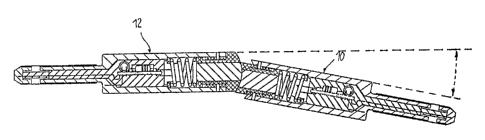
Fig. l A sectional view of a first coupling past of a light conductor coupling
in
exploded illustration (upper) and in assembled condition (Iower~,
Fig. 2 A sectional view of a second coupling part of a light conductor
coupling
in exploded illustration (upper) and in assembled condition (lower),
Fig. 3 A sectional view of the coupling parts of Pigs. T, and 2 in coupled
condition,
Fig. 4 The coupled coupling parts of Fig. 3, the sparing of which in the
direction
of the optical axis has been shortened,
Fig. 5 The coupled coupling parts of Fig. 3, the optical aces of which have
been
tilted relative to one another,
Fig. 6 A longitudinal section through the housing of the first coupling park
lFig. 7 A cross sectional view of the housing of the first coupling part,
Fig. S A cross sectional view of an alternative embodiment of the housing of
the
first COUpllng part,
6
CA 02447177 2003-10-28
Fig. 9 A functitonal sketch. of a sending device of the fizst coupling part,
Fig. 20 A functional sketch of a receiving device of the second coupling part,
and
Fig. Z1 A sectional view of a portion of a light conductor coupling for rail
~rehicles with two contact carriers, in each of which a coupling part of the
light conductor coupling is used.
DETAILED DESCRIPTION OF fif~iE pREFEItRED EMBODIMENT'S
Shown in Fig. l is a longitudinal sectional view of the first coupling part 10
of
a light conductor coupling according to a development of the present invention
in
exploded illustration (upper) and in assezmbled condition (lower). In Fig. 2
is shown
a longitudinal sectional illustration of the second coupling part 'IZ of the
same light
conductor coupling in exploded illustiration {upper) and xr~ assembled
condition
(lower}. Since the first and the second coupling parts 10 anal 12 are
identical in many
features, they will be described in comrrton in the following rwith similar
parts being
indicated by the same reference characters.
The coupling parts 10 and I2 each have a metal housing 14 with a sleeve-like
section 16 in which. a light conducting elexnenf 18 is axially slidably
supported. The
Iight conducting element 18 can be pressed into the sleeve-IilC.e section 16
of the
associated housing 14 against the biasing force of a spriztg 20. In place of
the spring
20, the Zight conducting element T8 can also be pneumatically biased by a gas
captured in the sleeve-like seciaon 1.6. Each light conducting element X8
includes a
light opaque sleeve 22 and a tx-ansparent core 24 received in the sleeve 22.
'~'he light conducting element 18 of the first coupling part has a spherically
concave end surface 2b facing atnray from the sleeve-like housing section 16
(Fig. l},
and the light conducting element 18 of fhe second coupling part 12 has a
spherically
conrrex end surface 26' (Fig. 2), the radius of curvature of which corresponds
to that
of the spherically concave end surface 2&. The spherically concave end surface
26
and the spherically convex end suxface 26' are formed not only in the
transparent
7
CA 02447177 2003-10-28
core 24 b~xt are also continued in the axial ends of the associated sleeves 22
of the
light conducting elements ~,8.
Guide grooves 27 are formed in the sleeves 22, which guide grooves receive
guide pins 28. The shifting movement of the light conducting element I8 is
thereby
limited by one of the ends of the guide groove 27 engaging a guide pin 28.
The inner space of the sleeve-like housing section I8 is made up of two
cylindrical sections, one being an inwardly lying section 30 and the other
being a
more outwardly lying section 32, the diameter of which is larger than that of
the
inwardly lying section 30. Between the cylindrical inner space sections 30 and
32 is a
shoulder 34 formed in the housing inner wall. In the outer inner space section
~2 are
located the Light conducting element 28 and the spring 20, which spring at one
exid
engages the Light conducting element T8 and with its other end engages a metal
xing
36 ~rhich in turn lies on the shoulder 34.
Tn the inner inner space section 30 in the case of the first coupling part 10
is a
sending device 38 (Fig. l) and in the case of the second coupling part is a
receiving
device 4D (Fig. 2). Each of the sending device 38 and the receiving device 40
has a
ground connecfiion 42 which is soldered to the sleeve-like section 1b of the
housing
14, and each has a signal terminal 44.
The housing ~4 has at its end facing a~nray from the light conducting element
18 a hollow connecting pin 46 with a ground connector section 48, a signal
connector
section 50, and Lying between them an insulating piece 52 which electrically
isolates
the sections 48 and 50 from one another. The signal Connector 44 is guided
through
the hollow space of the connector pin 46 and is soldered with the signal
connector
piece 50. The inner inner space section 30 and the hollow space of the
connector pin
46 are filled with pottant material illustrated in Figs.1 and 2 by cross
hatching.
Fig. 6 shows an enlarged cross sectional view of the housing 14 of the First
coupling part 10. As is to be seen in Fig. 6 the ground connector section 48
of the
connecting pin 46 has an external thread 54 formed on it, by means of which
the first
co~xpling pant ~0 is threadable into a socket at ground potential of a contact
carrier.
8
CA 02447177 2003-10-28
On the inner side of the ground connector section h8 is an internal thread 56
into
which the insulating piece 52 is threadable (see Fig.1). In the sectional
illustration of
Fig. b is further shown a bore 57 into which the ground connector 40 of the
sending
device 38 is soldered.
Fig. 8 shows a cross section through the housing ~.4 of the first coupling
part
taken along the line A-A of Fig. 6. As is to be seen, the sleeve like section
lb of the
housing 14 has a hexagonal external cross section to which a work tool is
applyable
to screw the coupling part 10 by way of its thxead 5~ into a socket. The
sleeve like
section 1& of the housing 14 has two recesses o~ 58 for the guide pins 28,
which have
already been described in connection with Figs.1 and 2. In place of two
recesses 58,
three recesses 60 can be provided which are displaced from one another by
120°, as is
shown in Fig. 7. rn this case the light opaque sleeve 22 has three
correspondingly
arranged guide grooves 27.
In Fig. 3 the first coupling part 10 and the second coupling pa~et 12 axe
shown
in coupled condition. In this condition, the end faces 26 and 26'' of the
associated
Iight conductor elements 7,8 are pressed onto one another so that the optical
signals
which are fed into the transparent core 2~ of the light conducting element 18
of the
first coupling part 10 are transmitted through the end faces 26 and 26' into
the
transparent core 24 of the light conducting element 18 of the second coupling
part 12.
Thereby the light opaque slee~res 22 of the light conducting elements 18 form
a light
ixnnel shielded from daylight.
Since the two light conducting elements 18 are each slidable in the housing of
14 of the associated coupling part x0 or 12 the coupling parts can be moved
somewhat away from and toward one another without disturbing the functioning
of
the signal coupling. In Fig. ~, for example, the coupling parts 10 and 12 of
Fig. 3
have been moved somewhat toward one another without that having changed the
positions of the light conducting elements 18 to one another, so that the
light
transmission remains undisturbed. The illustrated light conductor coupling
themfore allows a certain tolerance in the relative arrangement of the tw'o
coupling
parts 10 and ~.2 in the coupling direction, that is along the optical axes of
the light
conducting elements 18, which optical axes are formed by the middle axes of
the
9
CA 02447177 2003-10-28
Light conducting elements 18. Further, the spring pressure biased end faces 26
and
26' pz~event displacement of the optical axes of the Light cond~xcting
elements'18
against one another, that is they help to orient the coupling parts to ane
another and
to maintain the oriented positions.
In Pig. 5, the two coupling parts 10 and 12 are likewise shown in coupled
condition. Differently than in pigs. 3 and 4, in this case the coupling parts
10 and 12
are not aligned with each other, but instead are tilted relative to one
another. That
means that the optical axes of th.e Light conducting elements 3.~, each of
which
coincides with the symmetry axis of the associated transparent core 24, stand
at an
angle to one another. Because of their spherical shape, the end surfaces 26
and 26'
nevertheless lie without gap on one another, so that the attenuation of the
light upon
passage through the end surfaces 26 and 26' is held within limit. The light
conducti.~g coupling is therefore bendable to a certain degree, without such
bending
influencing its function, xhis is a large advantage in comparison to
customarily used
flat end faces which upon such a bending become lifted from one another so
fihat the
light transmission from one coupling part to the other becomes heavily
ateenuated.
In Pig. 5, the light conductor coupling is shown in its maximally bent
condition, in which the coupling parts are bent about 11° relative to
one another. In
the case of a further bending daylight would enter the light tcuu~el and
falsify the
optical signal. The limiting angle at which daylight penetrates into the light
tunnel
depends on the relationship of the wall thicknesses of the light opaque
sleeves in the
region of the end faces 26 and 26' to the radius of curvature of the end faces
26 and
26'. In the illustrated example, the wall thickness of the light opaque sleeve
22 of the
first coupling part 10 in the area of the end face 26 is smaller than, that of
the light
opadue sleeve 22 of the second coupling 12, and is therefore determinative of
the
value of the limiting angle. It measures about 1 / 5 of the radius of
curvature of the
spherical end surfaces 26 and 26'.
It is to be emphasized, that although the light conductor coupling shaven in
Pigs. l to 5 includes a sending device 38 and a receiving de~rrice 40, the
previously
described features, especially the spherical formation of the end surfaces 26
and 26'
are also assumed in the customary sense for light conductar couplings in which
no
TO
CA 02447177 2003-10-28
such active elements are provided. In this case light from one light conductor
is fed
into the light conducting element 18 of the first coupling part 10, is
transmitted
through its end surface 26 and through the end surface 2&' of the light
conducting
element I8 of the second coupling part 12 and is further conducted by a light
conductor connected with the light conducting element 1S of the second
coupling
part. The sending and receiving devices 3$ and 40 represent only an
advantageous
further development of the in~renfiion which is described in the following.
Fig. 9 shows a functional sketch of the sending device 38. As is to be taken
from this, an input voltage V;" is applied between the ground connection 42
and the
signal connection 44 through a scaling resistor 64 and is applied through a
high pass
filter, consisting of a capacitor &2 and a resistor 64, to a light emitting
diode 66, which
emits light corresponding to the applied voltage. The relationship between the
applied voltage V;n and the radiated power S of the light emitting diode 6& is
schematically represented in the diagram in the right por~,on of Fig. 9, whose
abscissa indicates time and whose ordinate gives the input voltage V~ and the
radiation power S in undefined units.
Fig.10 shows a functional sketch of the receiving device 40. The receiving
device 40 includes a photodiode 68 which in dependence an the intensity of the
incoming lightpxoduces a voltage, This voltage is suitably amplified in a
first circuit
section with the help of an operational amplifier 70, a resistor ?2, and a
capacitor 74,
and is inverted with the help of a further operational amplifier ~6 to an
output
voltage V~"=. The relation between the received emission power S' (which
multiplied
by an attenuation factor corresponds to the radiation power emitted from the
LED
66) and the Output Signal Vout Of the recei~ring device 40 is schematically
illustrated in
the diagram in the right portion of Fig.10, the abstissa of which again shows
fame
and the ordinate of which shows the received emission power S' and the output
voltage Vo~~ in undefined units.
The sending device 38 and the receiving device 40 are so designed that the
output signal Vp"~ of the receiving device 40 despite a possible attenuation
of the
transmitted optical signal corresponds to fine input volfage 'V~,. 'l~erefore,
even if the
optical signal transmitted between the coupling parts 10 and 12 is subjected
to a
11
CA 02447177 2003-10-28
certain attenuation, the effeci~:ve fransmitted electric signal V~,t is not
attenuated in
respect to the original signal V;~.
The electric input signal V;~" can for example be an electrical high frequency
signal which inside of two vehicles is conducted through a co-axial cable and
only to
suit the signal coupling is converted into an optical signal with the help of
the
sending device 38. The light conductor coupling with the active elements 38
and 40,
however, finds for example other uses if in the vehicle optical signals ate
already
transmitted through Iight conductors. These signals are then in the first
coupling
paxt 10 first converted to an electric signal which is then applied to the
sending
device 38. The output signal Vo"t of the receiving device 40 is then in the
second
coupling part again. converted into an optical signal and supplied to a
subsequent
light conductor.
Fig. 21 shows in sectional illustration a section of a conductor coupling for
use
xx~ combination with an automatic rail vehicle coupling. ~1n automatic
coupling is
used if the towed members have to be often coupled and de.-coupled. Then the
associated conductor coupling is so designed that ifs electrical and optical
contacts
are likewise automatically coupled along with the automatic coupling of the
towed
members.
The conductor coupling includes two contact carriers 78 and 80 in which,
along with a row of electrical contacts (not shown), the above-described
coupling
parts 10 and 12 of the light conductor coupling are also used. The eoupling
parfis at
20 and 12 are forwardly threaded into the contacf carriers 78 and 80 by means
of the
thread 54 of the connector pins 4~, whereby the thread 54 is subjected to
ground
potential. At the same time, the signal contact section 50 of the first
coupling part 7.0
corn.es into electrical contact with a schematically illustrated first signal
processing
unit 82 and the signal connector section 50 of the second coupling part 3,2
comes into
electric contact with a schematically illustrated second signal processing
unit $4.
In the illustrated exemplary embodiment the first signal-processing unit 82 is
supplied with electric signals over a co-axial cable 86 and optical signals
over a light
conductor 88. The optical signals of the light conductor 88 are converted into
12
CA 02447177 2003-10-28
electrical signals in a converter unit 90 and together with the electrical
signals of the
electrical conductor 86 are delivered to a control unit 92. Tn the control
unit 92 the
two inputted electrical signals are processed into a multiplexed signal which
is
transmitted to the signai connector 50 of the Bast coupling part. For this the
confrol
unit 92 has a microprocessor (not shown), which is constituted by an
industrial PC or
a so-called field programmable gate array (FPGA).
The control unit 92 further has a data input 94 through which further
information for the signal processing can be delivered. For example, through
the
data conductor 94, it can be signaled that already transmitted signals have
not been
completely received and sho~xld be sent again.
The conversion of the electric rnultipiexed signals into optical signals by
fhe
sending device 38 and their transmission from the first coupling part 10 to
the
second coupling part 12 fakes place in the way described above. From the
signal
connector 50 of the second coupling part 22, the electrical signals created in
the
receiving device 40 reach a control unit 9& of the second signal-processing
unit 84. In
the control unit 96 the multiplexed signals are divided into individual
signals. The
original ingoing signals from the electric conductor 86 are further conducted
by an
electrical conductor 98. The orxginai ingoing signals from the light conductor
88 axe
converted again into optical signals in a con~rerter unit 100 and are supplied
to a
Iight conductor 102.
By means of a further data conductor 104 signals from the control unifi 9b can
be further conducted, for example fault reports if signal errors have been
received.
The control unit 96 contains likewise an industrial PC or an FI7GA (not
shown).
The signal processing units 82 and 84 can also be contained in the housings 14
of the coupling parts. Further, the signal processing units 82 and 84 can each
be
connected with a transmission capable coupling part (similar to the first
coupling
part 10) and a receiving capable coupling part (similar to the second coupling
part
12). Then, signals can be transmitted from both sides of the coupling to the
other
side and the signal processing units of 82 and 84 can communicate with. one
another
in both directions.
13
CA 02447177 2003-10-28
The coupling parts 10 and 12 can above all be not only arranged in special,
contact carriers as shown in Fig.1I, but can also be arranged in the coupling
heads o~
a mechanical rail vehicle coupling, for example in an automatic intermediate
buffer
coupling (not shown). The above described insensitivity of the optical signal
coupling with respect to mechanical tolerazLCes makes this ~rrangen~.ent
possible,
which would not func~'ton in the case of a customary optical signal coupling.
Thereby in many cases a separate conductor coupling can be spared.
14
CA 02447177 2003-10-28 ,
REFERENCE CHARACTER LIST
IO - first coupling part
22 - second coupling part
14 - housing
16 - sIeeve-iilce housing section
18 - light conducting element
20 - spring
22 - Iight opaque sleeve
24 - transparent core
26, 26' - spherical end surfaces
27 -~ guide groove
28 - guide pin
30 .- inner inner space section
32 - outer inner space section
34 - shoulder
36 - metal ring
38 - sending unit
40 - receiving unit
42 - ground connector
44 - signal connector
46 - connector pin
48 - ground connector section
50 - signal connector section
52 - insulating piece
54 - external thread
56 - internal thread
57 - bore
58 - guide pin recess
6(l - guide pin recess
62 - capacitor
64 - resistor
66 - LED
68 - photodiode
CA 02447177 2003-10-28
70 - operational amplifier
72 - resistor
74 - capadtor
76 - operaf~onal amplifier
78 - contact carrier
80 - contact carries
82 - signal processing unit
84 - signal processing u~.it
86 - electric signal conductor
88 - light conductor
90 - signal converter
92 - control unit
94 - data conductor
96 - control unit
9S - electric signal conductor
200 - signal converter
102 - light conductor
104 - data conductor
26