Note: Descriptions are shown in the official language in which they were submitted.
CA 02447282 2003-11-17
WO 03/009317 PCT/IT02/00465
-1-
"SUPPORT WITH INTEGRATED DEPOSIT OF GAS ABSORBING
MATERIAL FOR MANUFACTUR.IING MICROELECTRONIC,
MICROOPTOELECTRONIC OR MICROMECHANICAL DEVICES"
The present invention relates to a support for manufacturing
microelectronic, microoptoelectronic or micromechanical devices with
integrated
deposit of gas absorbing material.
Microelectronic devices (also called integrated electronic circuits, indicated
in the field with the abbreviation ICs) are the base of the whole integrated
electronic industry. Microoptoelectronic devices comprise, for exalnple, new
generation infrared radiation (IR) sensors which, unlike traditional ones, do
not
require cryogenic temperatures for their operation. These Il2 sensors are
formed of
an array of semiconductor material deposits, for example silicon, arranged in
an
evacuated chamber. Micromechanical devices (better known in the field under
the
definition "micromachines" or its abbreviation MMs) are in developing step for
applications such as miniaturized sensors or actuators: typical examples of
micromachines are microaccelerometers, used as sensors to activate automobile
airbags, micromotors, having gears and sprocket wheels of the size of a few
microns (gin), or optic switches, wherein a mirror surface with a size of the
order
of a few tens microns can be moved between two different positions, directing
a
light beam along two different directions, one corresponding to the "on"
condition
and the other to the "off' condition of an optical circuit. In the following,
these
devices will also all be referred to with the general definition of solid
state
devices.
ICs are manufactured by a technology comprising operations of deposit on a
planar support of layers of material with different electric (or magnetic)
functionality, alternated to selective removals thereof. The same techniques
of
depositions and selective removals are applied to microoptoelectronic or
micromechanical devices construction as well. These are generally contained in
housings formed, in their turn, with the same techniques. The support most
commonly used in these productions is a silicon "slice" (said "wafer" in the
field),
CA 02447282 2003-11-17
WO 03/009317 _ PCT/IT02/00465
-2-
about 1 mm thick and with a diameter up to 30 cm. On each of these wafers a
very
high number of devices is constructed; then, at the end of the manufacturing
process, from these slices are separated, by mechanical or laser cut, the
single
devices in the case of micromachines, or parts including an array of some tens
of
devices in the IR sensors case.
The deposition steps are carried out with such techniques as chemical
deposition from vapor state, generally defined "CVD" from "Chemical Vapor
Deposition"; physical deposition from vapor state or "PVD", from "Physical
Vapor Deposition", the latter conunonly indicated also as "sputtering".
Generally,
selective reniovals are carried out through chemical or physical attacks with
proper masking, as it is well known in the field.
The integrated circuits and the micromachines are then encapsulated in
polymeric, metallic or ceramic materials, essentially for mechanical
protection
reasons, before being inserted in the final destination apparatus (a computer,
an
automobile, etc.). On the contrary, IR radiation sensors are generally
comprised in
a chamber, facing one wall thereof defined as "window", transparent to the IR
radiation.
In some kinds of integrated circuits it is important to be able to control the
gas diffusion in solid state devices: it is for example the case of
ferroelectric
memories, wherein hydrogen, diffusing through device layers, can reach the
ferroelectric material (generally a ceramic oxide, such as lead titanate-
zirconate,
strontium-bisinuth tantalate or titanate, or bisinuth-lantllanum titanate),
altering its
correct behavior.
Still more important is gas control and elimination in IR sensors and in
microinachines. In the case of IR sensors, the gases possibly present in the
chamber can either sorb part of the radiation or transport heat by convection
from
the window to the array of silicon deposits, modifying the measure. In
micromachines, the mechazical friction between gas molecules and the moving
part, due to the very small size of the latter, can lead to sensible
deviations from
the device's ideal operation; moreover, polar molecules such as water can
cause
phenomena of adhesion between the moving part and other parts, for example the
CA 02447282 2003-11-17
WO 03/009317 PCT/IT02/00465
-3-
support thereof, thus causing the device's failure. In the IR sensors with
arrays of
silicon deposits or in the micromachines, it is therefore fundamental to be
capable
of ensuring the housing to remain in vacuum for the whole device life.
lii order to minimize the gas amount in these devices, their production is
usually conducted in vacuum chambers and resorting to pumping steps before the
packaguZg thereof. Anyway the problem is not coinpletely solved in this way,
because the same materials which form the devices can release gases, or these
can
permeate from outside during the device life.
To remove also the gases entering in solid state devices during their life, it
has been proposed the use of materials that can sorb these. These materials
comprise those commonly referred to as "getters", generally metals such as
zirconium, titanium, vanadiuin, niobium or tantalum, or alloys thereof with
other
transition elements, rare earths or aluminum, having a strong chemical affmity
towards gases such as hydrogen, oxygen, water, carbon oxides and in some cases
nitrogen; and the drier materials, specific for moisture absorption, among
which
mainly the oxides of alkali or alkaline-earth metals. The use of materials
absorbing gases, particularly hydrogen, in ICs, is described for instance in
patent
US-A-5,760,433 and in published Japanese patent applications JP-11-040761 and
JP-2000-40799; their use in IR sensors is described for example in patent US
5,921,461; finally, the use of gas absorbing materials in micromachines is
described for example in the article "Vacuum packaging for microsensors by
glass-silicon anodic bonding" by H. Henmi et al., published on technical
journal
Sensors and Actuators A, vol. 43 (1994), at pages 243-248.
Localized deposits of gas absorbing materials can be obtained by CVD or
sputtering during solid state devices productive steps. However, this
procedure is
not very appreciated by manufacturers of these devices, since gas absorbing
material deposition during devices production implies the need that the total
process is added with a step of localized deposition of this material,
generally
carried out through the operations of resin deposition, resin local
sensitization
through radiations (generally UV), selective removal of the photosensitized
resin,
gas absorbing material deposition and subsequent reinoval of the resin and of
the
CA 02447282 2003-11-17
WO 03/009317 PCT/IT02/00465
=4-
absorbing material thereon deposed, leaving the gas absorbing material deposit
in
the area from which the photosensitized resin had been removed. Moreover, the
gas absorbing material deposit in the production line has the disadvantage
that
increasing the nuinber of different steps of the process and of the materials
therein
used, also the risk of "cross-pollution" among the different chambers in which
said different steps are carried out increases, with following possible
increase of
waste products because of contamination.
The object of the present invention is to overcome the above-described
problems of the prior art and, particularly, to simplify the manufacturing of
solid
state devices.
This object is achieved according to the present invention with a support for
manufacturing microelectronic, microoptoelectronic or rnicrornechanical
devices
with integrated deposit of gas absorbing material, formed of a base having the
fu.nction of a mechanical backing, a continuous or discontinuous deposit of a
gas
absorbing material on a surface of said base, and a layer totally covering
said gas
absorbing material deposit, made witli a material compatible with the
production
of microelectronic, inicrooptoelectronic or microinecllanical devices or parts
thereof.
The support of the invention is practically similar to silicon wafers
cominonly used in industry, having, however, gas absorbing material (in the
form
of continuous layer or discrete deposits) "buried" under the surface on which
the
microelectronic or micromechanical devices are formed through above-mentioned
teclmiques of solid inaterials deposition and removal.
The invention will be described below with reference to the drawings in
which:
- Fig. 1 shows a perspective, partially cut-out view of a first possible
support
according to the invention;
- Fig. 2 shows a perspective, partially cut-out view of a second possible
support according to the invention;
- Figs 3 to 11 represent some ways to use the supports of the invention.
For the sake of description clarity, in the drawings the supports according to
CA 02447282 2003-11-17
WO 03/009317 PCT/IT02/00465
-5-
the invention are represented with an extremely exaggerated height-diameter
ratio,
with respect to real dimensions. Moreover, in the drawings, supports are
always
represented with a wafer geometry, that is a low disk of material, because
this is
the geometry commonly adopted by the producers of solid state devices, but
this
geometry could be also different, for example square or rectangular.
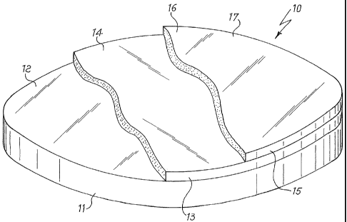
Figure 1 shows, in a partially cut-out view, a support of the invention in its
siinplest embodiment. The support, 10, comprises a base, 11; this has the only
function of mechanical backing the support and the devices deriving therefrom,
and the thickness of support 10 (of the order of one inillimeter) is given
nearly
completely from this base's thiclcness. On surface 12 of base 11 there is a
continuous layer 13 of a gas absorbing material, 14, whose upper surface is
covered witli another layer 15 of a material 16 compatible with the ICs or MMs
production process, which are produced on the upper surface 17 of layer 15.
The material of base 11 can be a metal, a ceramic, a glass or a
semiconductor, preferably silicon.
Material 14 can be any la-iown material chosen among the materials
commonly referred to as getters, capable of sorbing various gas molecules, and
the drier materials, specific for moisture absorption.
In the case of a getter material, this can be for example a metal as Zr, Ti,
Nb, Ta, V; an alloy among these metals or among these and one or more
elements,
chosen ainong Cr, Mn, Fe, Co, Ni, Al, Y, La and rare-eartlls, such as binary
alloys
Ti-V, Zr-V, Zr-Fe and Zr-Ni, tem.ary alloys Zr-Mn-Fe or Zr-V-Fe or alloys with
more components. Preferred getter materials for this application are titanium,
zirconium, the alloy having weight percentage composition Zr 84%-Al 16%,
produced and sold from applicant under the name St 101 , the alloy having
weight percentage coinposition Zr 70%-V 24.6%-Fe 5.4%, produced and sold
from applicant under the name St 707 and the alloy having weight percentage
composition Zr 80.8%-Co 14.2%-TR 5% (wherein TR is a rare-earth, yttritun,
lanthanum or mixtures thereof), produced and sold from applicant under the
name
St 787. Getter material layer 13 can be obtained by different techniques, such
as
evaporation, deposition from metallorganic precursors, or by techniques known
in
CA 02447282 2003-11-17
WO 03/009317 PCT/IT02/00465
-6-
the field as "laser ablation" and "e-beam deposition"; preferably this layer
is
obtained by sputtering.
hz the case of drier materials, these are preferably chosen among the oxides
of alkali or alkaline-earth metals; particularly preferred is the use of
calcium
oxide, CaO, that does not pose safety or environmental problems during the
phases of production, use or disposal of devices containing it. A layer 13 of
oxide
may be obtained for instance through the so-called "reactive sputtering"
technique, depositing the alkali or alkaline-earth metal of interest under an
atmosphere of a rare gas (generally argon) in which a' low percentage of
oxygen is
present, so that the metal is converted to its oxide during deposition.
Layer 13 can have a thickness within the range of about 0,1 and 5 m: with
thickness values lower than the indicated ones, the gas sorption capacity of
layer
13 is excessively reduced, while with higher thickness values deposition times
are
extended without real advantages on sorption properties.
Material 16 is one of the materials which are usually used as substrate in
solid state devices production; it can be a so-called III-V material (for
example,
GaAs o InP), or preferably silicon. Layer 16 can be obtained by sputtering, by
epitaxy, by CVD or by others techniques known in the field. The thickness of
layer 16 is generally lower than 50 m and preferably within the range of
about 1
to 20 m. This layer performs two functions: it protects the gas absorbing
material
from the contact with gases until this latter is exposed (by partial and
localized
removal of layer 16), and acts as an anchorage for the layers which are
subsequen.tly deposed thereon to construct ICs, microoptoelectronic devices or
MMs, or it can be even itself the layer in which these devices are formed (for
example the micromachine moving parts can be obtained in this layer by removal
of parts thereof). The upper surface of layer 16 can also be treated so as to
modify
its chemical composition, for example fonning an oxide or a nitride, in view
of
the following operations of devices production.
Figure 2 shows a second possible embodiment of the support according to
the invention; also in this case the support is represented partially in cut-
out view,
and besides in this case also the lateral dimensions of the various deposits
on the
CA 02447282 2007-02-28
-7-
base of gas absorption material are exaggerated for the sake of clarity.
Support 20
comprises a base 11. In areas 22, 22', ... of surface 12 of this base discrete
deposits,
24, 24', ..., of gas absorbing material 14 are obtained; these are then
covered with a
layer 26 of material 16.
Deposits 24, 24', ..., are as thick as layer 13 of support 10. These deposits
are, however, discrete, and have lateral dimensions generally lower than 500
m
and variable within wide ranges depending on the final destination device: for
example, if use is expected in ICs, the lateral dimensions will be within the
range
of some micron or less, while in the case of MMs, these dimensions can be
comprised between a few tens and a few hundreds of microns.
Layer 26 has a variable thickness, lower in the areas over deposits 24, 24',
and higher in the areas cleared from these deposits, adhering to surface 12 in
these areas. The thickness of this layer in the areas over the deposits has
the same
values of layer 15 of support 10, while in areas clear from deposits 24, 24',
..., its
thickness will be increased of the thickness of these deposits. To help
adherence,
layer 26 is preferably made with the same material of base 11; the preferred
combination is silicon (mono-or polycrystalline) for base 11, and silicon
grown
through epitaxy for layer 26.
Figures 3 and 4 show a possible use of support 10 in ICs production. On
upper surface 17 of support 10, formed of a layer 15 for example of silicon,
solid
state microelectronic circuits, schematized as elements 30, 30', ..., are
obtained
with known techniques. Support 10 is then cut along dotted lines in figure 3,
thus
obtaining single ICs devices: one of these is schematized in figure 4, showing
a
integrated circuit 40 obtained on a part of support 10 that has integrated,
"buried"
under surface 17, a layer 13 of gas absorbing material 14. This layer 13 is
capable
of sorbing gases, especially hydrogen, which may diffuse through the different
layers of the device, thus preventing or reducing the contamination of
integrated
circuit 40.
In the case of MMs production, on surface 17 of the support are produced
CA 02447282 2003-11-17
WO 03/009317 PCT/IT02/00465
-8-
structures, schematized in figure 5 as elements 50, 50', ..., which comprise
the
mobile parts of the micromachine. When the production of structures 50, 50',
...
(including leads for the electric connection of every single micromachine with
the
outside, not showed in the drawing) is finished, the support is subjected to a
localized removal operation of layer 15, in areas of surface 17 which are
cleared
from said structures, thus forming passages 51, 51', ..., which expose the gas
absorbing material 14; then a covering element 60 is placed over the so
treated
support 10, (the assembly of this and support 10 is showed in cross-section in
figure 6), this element will be realized, generally, with the same materials
of base
11 and it should be easily fixable to surface 17 (the use of silicon is
preferred):
this element 60 can have hollows, 61, 61', ..., (case shown in f'igure) in
correspondence with areas wherein, on support 10, structures 50, 50', ...,
have
been obtained and portions of layer 13 have been exposed; in particular, each
of
said hollows will be such that, when support 10 and elenlent 60 are fixed
together,
a space 62 is obtained wherein a structure like 50, 50', ..., and a passage 51
giving
access to material 14 are contained, so that this latter is in direct contact
with
space 62 and is able to sorb gases possibly present or released during time in
said
space. Finally, single micromacliines are obtained by cutting the assembly
made
up of support 10 and element 60 along their adllesion areas.
In a variation of the lnicroinachines production process sumtnarized above,
the localized removal of layer 15 is carried out before the l.nanufacturing
steps of
structures 50, 50', .
In another variation of the process outlined above, whose final result is
micromachine 70 shown in figure 7, the support of the invention is used as
element 60. In this case, the substrate on which the micromachine is formed is
a
traditional one, without integrated gas absorbing layer. Support 10 of the
invention is subjected to a localized reinoval treatment of layer 15, thus
forming at
the same time a hollow 71 constituting space 72 for housing mobile structure
73,
and the passage giving access to material 14.
The use of a support of type 20 will be illustrated only in relation to the
use
as a support on whose surface a micromachine is formed (use similar to that
CA 02447282 2003-11-17
WO 03/009317 PCT/IT02/00465
-9-
represented in figures 5 and 6), but, obviously, this can also be used as
support for
ICs production (as described with reference to figures 3 and 4) or as a
covering
element in micromachines (as described with reference to figure 7). Support 20
is
subjected to a localized removal treatment of layer 26 in oorrespondence to
deposits 24, 24, ..., thus obtaining on the support passages 80, 80', ..., as
shown in
section in figure 8, ready for the sequence of steps for micromachines
pToduction.
Moving structures (schematized as elements 90, 90') of figure 9 are then
formed
on this support; afterwards, a covering element 100 is fixed to support 20, in
areas
cleared from moving structures 90, 90', ... and from passages 80, 80', ...,
thus
obtaining assembly 101 shown in section in figure 10; finally, by cutting
assembly
101 along lines (dotted in figure) comprised in adhesion areas between support
20
and element 100, the micromachine 110 shown in section in figure 11 is
obtained.
,Due to its way of use, support of type 20 must be produced when final
application is known. In particular, especially in case of the inicromachines,
it is
important to kn.ow the lateral size of the inoving structures (50, 50', ...,
73 or 90,
90'...) as well as the lateral size of the hollows (61, 61', ... or 71) to be
produced
next, so to be able to define correctly the lateral size and reciprocal
distance of
deposits 24, 24', ...; in this way it is assured that the hollows giving
access to the
gas absorbing material do not'interfere with moving structure, but also that
they
are contained in the perimeter of space 62 or 72 wherein the micromaclline is
housed. This correct sizing can be carried out by obtaining, from final
circuits
producers, drawings, even preliminary, of devices to be produced on support
20.