Note: Descriptions are shown in the official language in which they were submitted.
CA 02447373 2003-11-10
WO 03/003619 PCT/US02/20112
TITLE
REDUNDANT OPTICAL DEVICE ARRAY
FIELD OF THE INVENTION
This invention relates to arrays of optical devices such as lasers and
photodetectors
and, more particularly, to arrays of optical devices having increased yield
and longer lifetime.
BACKGROUND OF THE INVENTION
Over the past few years the dramatic increase in the use of fiber optics in
communications systems has created a tremendous need for both cheaper and more
reliable
optical components. Unfortunately, the limited materials usable to create
acceptable laser
diodes and photo detectors for use in such devices effectively limits the mean
time between
failures (MTBF) that can be achieved for such devices.
Typically diode lasers or photodetectors are fabricated by growing the devices
on a
semiconductor substrate. Depending upon the particular devices and there
design, this may
entail the use of known techniques such as liquid-phase epitaxy, metal-organic
vapor-phase
epitaxy, molecular beam epitaxy. Each of these techniques has its advantages
and
disadvantages in terms of the quality, reliability, and frequency of defect
occurrence.
Once the active portion of the device is produce by the epitaxial growth
process, the
devices are then further processed into device chips. During these processes
dielectric films
and various metals are deposited on the semiconductor , for example, to
isolate parts or create
contacts. Finally, photolithography and/or chemical or physical etching are
used to finish the
devices. Once the device structures are fully formed in the semiconductor
wafer, each device
is separated from the wafer, for example, by cleaving.
FIGS. 1A and 1B show two variants of an example optical device of the prior
art, a
semiconductor laser diode. The specific devices 110, 120 shown in FIGS. 1A and
1B are
vertical cavity surface emitting lasers (VCSEL). As shown, each device 110,
120 is
contained in an approximately 200 micrometer (micron) square area of semi-
conductor
material. Each device 110, 120 has an optical window 112, 122 of approximately
17-19
micron diameter. The device 110 ,120 is connected via a trace 114, 124 to a
bonding pad
116, 126 approximately 100 microns square. In Fig. 1A, the bonding pad serves
as the
positive ("+") contact and in FIG. 1 B, the bonding pad serves as the negative
("-") contact.
FIG. 2 shows multiple individual VCSELs that have been combined to form at
least a
2 X 3 array of lasers. The devices 200 are arranged so that the spacing
between each laser
1
CA 02447373 2003-11-10
WO 03/003619 PCT/US02/20112
(i.e. the "pitch") is approximately 250 microns. Such arrays can be relatively
reliable,
because each individual laser device 200 can be operationally tested before it
is integrated
into the array. However, once the array is created, if an individual element
fails, either the
entire array must be replaced or the array becomes degraded because there is
no easy way to
repair it.
Moreover, even if the array is created from macrostructures, for example, so
that there
are 1 X 4 discrete devices on a common carrier. If any one of the devices is
defective, the
entire carrier becomes useless or the individual good devices must be removed
from it and
used individually.
All of the above results in arrays that are both costly to produce and, in
their overall
configuration, have an overall MTBF of the least reliable device in the array.
Thus there remains a need in the art for a way to produce a chip incorporating
an
array of optical devices that is less costly to produce.
There remains a further need in the art for an array that is easy to repair at
low cost.
BRIEF DESCRIPTION OF THE DRAWINGS
FIGS. 1A and 1B show two variants of an example semiconductor laser diode
optical
device of the prior art;
FIG. 2 shows multiple VCSEL's of FIG. 1 arranged in an array according to the
prior
art;
FIG. 3 shows a redundant laser pair from an array in accordance with the
invention;
FIG. 4A shows a group of four redundant lasers from an array according to the
mvenhon;
FIG. 4B functionally shows contacts for the group of FIG. 4A;
FIG. 5 shows the functional components of an opto-electronic chip suitable for
use in
accordance with the invention;
FIG. 6 shows the chip of FIG. 5 employing pairs of redundant lasers according
to the
invention;
FIG. 7 shows an alternative variant to the chip of FIG. 6;
FIG. 8 shows the chip of FIG. 5 employing groups of four redundant lasers
according
to the invention;
FIG. 9 shows the chip of FIG. 5 employing pairs of redundant photodetectors
according to the invention;
FIG. 10 shows a device of FIG. S employing groups of four redundant photo
detectors
according to the invention;
2
CA 02447373 2003-11-10
WO 03/003619 PCT/US02/20112
FIG. 11A shows one functional example of circuitry for selecting from among
two or
more redundant devices according to the invention;
FIG. 11B shows another functional example of circuitry from among two or more
redundant devices according to the invention;
FIG. 12 functionally shows an opto-electronic transceiver incorporating the
invention;
and
FIG. 13 is a functional block diagram of example automatic failover circuitry
for a
group of two devices.
SUMMARY OF THE INVENTION
We have devised a way to create electro-optical chips that avoid the problems
of the
prior art.
In particular, we have created a way to deploy large numbers of optical
devices in a
manner which provides a higher overall yield and greater reliability.
Depending upon the
particular implementation, further advantages such as reparability after
deployment, and
performance optimization can be achieved.
One aspect of the invention involves an optical module having multiple optical
devices. At least two of the multiple optical devices are a group. Each of the
optical devices
in the group are individually selectable relative to the others. The optical
module also has a
controller, coupled to the devices such that the controller can select which
of the devices in
the group will be active at a given time.
Another aspect of the invention involves a method of creating an optical chip,
having
redundant devices, for use in an opto-electronic unit involves growing active
portions of
multiple optical devices on a wafer, processing the wafer to create complete
optical devices,
creating individual optical devices, grouping the devices; and connecting the
devices in
agroup to a control circuit such that, common data can be received by any of
the devices in
the group but the common data will only be handled by the device in the group
that is active.
Yet another aspect of the invention involves a communications network that has
a
first transmitter having a number of usable channels, a first receiver, and
optical fibers
connecting the first transmitter to the first receiver. The first transmitter
has multiple lasers,
at least some being selectable as either active or backup lasers. The multiple
lasers are
controllable such that, if a specific channel is in use by an active laser and
a laser failure
occurs for that channel, a redundant laser can be substituted for the active
laser and, after the
substitution, the specific channel can be used using the redundant laser.
3
CA 02447373 2003-11-10
WO 03/003619 PCT/US02/20112
These and other aspects described herein, or resulting from the using
teachings
contained herein, provide advantages and benefits over the prior art.
The advantages and features described herein are a few of the many advantages
and
features available from representative embodiments and are presented only to
assist in
understanding the invention. It should be understood that they are not to be
considered
limitations on the invention as defined by the claims, or limitations on
equivalents to the
claims. For instance, some of these advantages are mutually contradictory, in
that they cannot
be simultaneously present in a single embodiment. Similarly, some advantages
are applicable
to one aspect of the invention, and inapplicable to others. Thus, this summary
of features
and advantages should not be considered dispositive in determining
equivalence. Additional
features and advantages of the invention will become apparent in the following
description,
from the drawings, and from the claims.
DETAILED DESCRIPTION
FIG. 3 shows a portion 300 of a two dimensional array of lasers 302 created
according
to the principles of the invention. The portion shows two individual laser
devices 302 bonded
via contact pads 304 to an electronic chip 306. As shown, the devices 302 are
bottom
emitting laser devices that have been flip chipped bonded to the electronic
chip, although as
will be apparent from the description herein, bottom receiving, top emitting
or top receiving
devices can be used as well, particularly if the approaches of the commonly
assigned U.S.
patent applications entitled Opto-Electronic Device Integration filed
concurrently herewith
(which are incorporated herein by reference) is employed as part of the
process.
Because the substrates 308 have not been removed or excessively thinned,
emissions
of the lasers occur via access ways 310 created in the substrate 308 on which
the laser
devices were supported to allow for close optical access to the devices. The
spacing between
the access ways, i.e. the pitch, is such that each of the lasers 302 can be
either directly
coupled to a single optical fiber, or directed into a common optical fiber,
for example, by
focusing the light output using a micro lens or guiding the light using an
optical waveguide.
Thus, depending upon the particular lasers and fibers used, the pitch between
the two lasers
can be as small as 5-10 microns for direct lasing into a single mode fiber or
50-100 microns
for direct lasing into a multimode fiber. Alternatively, if an optical wave
guide or focussing
lens is used, the inter-device pitch becomes less important and may be as much
as a 100
microns or more as needed.
4
CA 02447373 2003-11-10
WO 03/003619 PCT/US02/20112
During device creation the lasers are separated into individual devices by
patterning
the laser wafer prior to bonding with the electronic chip, for example as
shown in the
incorporated commonly assigned application entitled, Opto-Electronic Device
Integration.
Additionally, the devices are patterned with grouping trenches 312 which
physically and
S electrically define groups by creating boundaries separating individual
groups 314 of
redundant devices. The grouping trenches 312 ensure isolation among the
individual groups
while allowing for carrier movement among the devices within the group via the
electrically
conductive substrate 308. In this manner a group is physically created as
either multiple
discrete devices or a single "device" having multiple active regions.
All the devices in a group 314 share a common connection (either the positive
or
negative contact) so that any signal to be sent or received by any of the
devices can be sent or
received by any other of the devices in the group irrespective of which one is
selected as
being active using the contacts. In other words, if three lasers constitute a
group in an optical
module, such as an optical transmitter, they will be coupled to a single
optical fiber, all have
one contact in common and all have individual opposite polarity contacts. If
the transmitter
were to send data through the optical fiber, the same signal would be sent
irrespective of
which laser was active at the time. Moreover, from the perspective of the
functions of any
prior art optical transmitter, the transmitter incorporating the invention can
be oblivious to
which laser in the group is active. Advantageously, the purchaser or user of
the transmitter,
or any other device employing the invention, need not know it contains device
redundancy.
The features and elements that allow selection of the particular active laser
can be wholly
transparent to anyone other than the manufacturer or can be made accessible to
third parties
to varying degrees.
FIG. 4A shows a portion of a laser array employing groups 400 of four lasers
402 as a
redundant group. As shown, the individual devices have been separated through
patterning
of separation trenches 404 which isolate the individual device contacts 406,
and groups 400
have been created by patterning of grouping trenches 408 which isolate the
common contact
410 from the common contacts) of other neighboring groups. As with FIG. 3,
access ways
310 are provided through the substrate to provide for close optical access to
the lasers. FIG.
4B is a functional representation of the group of FIG. 4A but showing the
discrete contacts
406 for each laser and the substrate 308, which is used as the common contact.
Advantageously, by grouping the lasers in fours, significant flexibility can
be
obtained. For example, the best two of the four lasers can be used as a
redundant pair with or
without the remaining two lasers serving as back up devices for either laser
in the pair, the
CA 02447373 2003-11-10
WO 03/003619 PCT/US02/20112
best of the four lasers can be employed as a primary laser with each of the
remaining three
being available should the primary laser fail, or should any individual laser
in the group be
bad, it can be disregarded entirely.
FIG. 5 shows the functional components of an opto-electronic device 500
suitable for
employing the principles of the invention. Functionally, the device includes a
laser portion
502 which contains an array of individual lasers. The device also includes a
detector portion
504 which includes an array of individual photodetectors. A control portion
506 is provided
which contains the control electronics for accessing the individual lasers
and/or detectors.
Additionally, a storage portion 508 can optionally be provided, as will be
described in greater
detail below. Finally, the device includes an interface portion 510 through
which the opto-
electronic chip may be electrically or programmatically connected to other
devices or control
electronics. Depending upon the particular implementation, the interface
portion 510 may be
functionally located between the control portion 506 (and/or the storage 508
if this option is
used) and the devices 502, 504, for example where the control 506 and/or the
storage 508 can
be provided by a third party. In other variants, the interface 510 may provide
a way to bypass
or override either or both of the control portion 506 and/or storage 508 if
either or both are
present.
Functionally, the control portion 506 is, in whole or part, the "brains" of
the opto
electronic chip 500. At least, it is the brains with respect to the redundancy
feature. The
control portion 506 is physically made up of the hardware used to activate the
individual
devices based upon, for example, information stored in the storage, and/or to
specify, update
and/or change the stored information to initialize the chip or reprogram it
following a failure.
Depending upon the particular implementation, the control portion will be a
processor, for
example, a microprocessor operating under program control, a state machine,
hard wired
circuitry or some combination thereof.
Depending upon the particular implementation, the storage will be in the form
of
static random access memory (SRAM), dynamic random access memory (DRAM or
RAM),
or some form of read only memory (ROM) which may be, for example, a device
such as a
programmable read only memory (PROM), an electronically programmable read only
memory (EPROM), an electronically erasable programmable read only memory
(EEPROM),
a programmable logic device (PLD), etc. to name a few.
The storage 508 is accessible by the control portion 506 and is configured to
allow the
active device in each group to be specified. Optionally, the storage 508 can
be further
configured to keep track of redundant (i.e. back-up) devices and, as a further
option, can be
6
CA 02447373 2003-11-10
WO 03/003619 PCT/US02/20112
configured to specify the hierarchy or ordering for bringing on-line the
remaining devices in
the group if needed.
For example, Table 1 shows a simple table that can be employed for groups of
device
pairs. Each pair has a group address or identifier that uniquely identifies,
directly or
S indirectly, each discrete group. A single bit is used to designate the
active device, for
example, with a binary 0 representing the first device in the group and a
binary 1 representing
the second device in the group.
Group AddressActive Device
Xo
'1'A13LE 1
Table 2 shows an alternative arrangement for identifying the active device in
the
storage. As with Table 1, an address or identifier uniquely identifies the
particular group.
Associated with that address is a rivo-bit binary number, where each bit
corresponds to one
device in the group and is used to signify whether that device is to be
active.
Group AddressActive Device
XiXo
TAB LE 2
For example, a bit pattern of 00 would specify that neither device is active.
Bit
patterns of O1 or 10 would indicate that one or the other device in the pair
is active.
Depending upon the particular implementation, a bit pattern of 11 could, for
example, be
used to activate both devices for some special case or could simply be an
invalid state.
Table 3 shows a similar arrangement for a chip having groups made up of four
devices. In this case, a similar two bit binary number is used except, the
actual number in
binary is used to indicate the active device.
Group AddressActive Device
X~Xo
TAB LE 3
7
CA 02447373 2003-11-10
WO 03/003619 PCT/US02/20112
For example, a 00 would indicate that the first device in the group is active,
a O1
would indicate the second device in the group is active. A 10 would indicate
that the third
device is active and a 11 would indicate that the fourth device is active.
Table 4 shows a more complex arrangement for keeping track of the active
devices in
a particular array having individual four device groups. As shown Table 4
includes an
address as noted above. In addition, an eight-bit binary number
(X,XoA~AoB~BoC~Co) is
used to identify the particular laser device in the group that is the primary
(i.e. active) device
as well as a hierarchy for the remaining devices in the group.
Group Primary SecondaryTertiaryQuartic
AddressDevice Device Device Device
XIXo A~Ao BIBo C,Co
l
TABLE 4
For example, for a particular address, an entry of 01110010 would indicate
that the
second device (O1) is active. In the event that device was unusable or failed,
the next device
to be brought on-line is the fourth device. If that device were to fail, the
next devices brought
on-line thereafter would be, in order, the first followed by the third.
As can be appreciated, there are numerous ways other ways to identify active
devices
and/or specify alternative devices, either by employing some variant or
combination of the
above examples, or creating some other methodology, for example, by
designating each laser
with a unique address (irrespective of its group) and maintaining a list of
the addresses for the
lasers in each group in the order they are to be brought on line or providing
space for settings
for each laser, such as bias and modulation, and filling the setting
information in for active
lasers and/or setting the bias and/or modulation settings to zero and/or an
invalid value to
deactivate a laser.
In an alternative implementation, involving no storage for device selection,
the
devices incorporate fusible links that can be used to bring a device on- or
off line. For
example, each device may incorporate two fusible links. Initially, neither
link is blown so the
device is inactive but available. To bring a device on line, circuitry is
activated that causes a
particular link to blow and renders the device active. In the event that
device dies some time
in the future, other circuitry can be enabled to blow the remaining link,
rendering the device
inactive. A redundant device in the group can then be brought on-line by
blowing the first
link for that redundant device in a similar manner.
8
CA 02447373 2003-11-10
WO 03/003619 PCT/US02/20112
Still other alternative implementations use a combination of storage and hard
wiring
or fusible links to accomplish the functions of the control and/or storage.
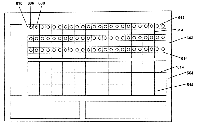
FIG. 6 shows an opto-electronic device of the type shown in FIG. 5 in greater
detail
and constructed according to the principles of the invention. As shown, the
detector portion
604 is made up of 36 individual detectors and the laser portion 602 is made up
of 36 pairs of
redundant lasers. As shown, the individual lasers 606, 608 in a group 610 are
separated by
device trenches 612 and the groups are separated from each other by grouping
trenches 614.
In addition, there are available areas 616 between adjacent rows of the paired
redundant lasers. Depending upon the particular implementation, those areas
may be wholly
unused, may be occupied by lasers of other wavelengths than those of the
redundant pair, or
may represent additional lasers of the same type as the redundant pairs which
have been
disabled for one reason or another.
FIG. 7 shows an opto-electronic chip 700 similar to that of FIG. 6 except that
the
array has been patterned as if four discrete devices were present to make up a
group 702.
However, each group contains only two lasers 704, 706.
FIG. 8 shows a chip 800 similar to the chip of FIG. 6 except that each
individual
group 802 is now made up of four individual lasers 804, 806, 808, 810.
FIG. 9 shows a chip 900 like the device of FIG. 5 but having pairs 902 of
redundant
photodetectors. As shown, the photodetectors are grouped, like the lasers of
FIG. 6, by
grouping trenches 904 and individual photo detectors 906, 908 within a group
are separated
by device trenches 910.
It is important to note in connection with redundant detectors, that the use
of
redundant detectors will require that either some additional device be used to
redirect the
incident light from one detector to the other detector in order to switch
between them.
Alternatively, the light can be defocused or defracted so as to be incident on
all pertinent
devices on both (in this case) as required. As should be apparent however, if
redundant
detectors are used and no light redirection is provided the system must be
capable of
accepting the losses due to such defocusing or defracting because the amount
of incident light
will be reduced exponentially as it is defocused to a larger and larger area
to accommodate a
larger number of redundant devices or a large pitch among them.
FIG. 10 shows a chip 1000 having an array 1002 similar to the array of FIG. 9
except
that the array of FIG. 10 incorporates four redundant detectors 1004, 1006,
1008, 1010 per
group.
9
CA 02447373 2003-11-10
WO 03/003619 PCT/US02/20112
Having shown a number of functional variants according to the invention, some
examples of aspects usable for specific implementations will now be provided.
FIG. 11A shows one functional example of a circuitry arrangement for selecting
from
among two or more redundant devices according to the invention. In variants
according to
this example, a common data signal source 1102 is connected to all of the
lasers 1104 in a
group. As shown two or more lasers are in the group. A multiplexor 1106 (for 1
-to- 1
connections) or a selector (for 1 -to- 1 or more connections) is inserted
between the power
source 1108 for the lasers and the lasers themselves. The control information
(whether bit
based or bias/modulation based) is used by the control portion 1110 to select
which laser
receives power. Alternatively, in some variants, the multiplexor can be
replaced with a
selector that can select any one or more of the lasers.
FIG. 11B shows another functional example of a circuitry arrangement from
among
two or more redundant devices according to the invention. In variants
according to this
example, a signal source 1 I 12 is amplified by an amplifier 1114 and
connected to the lasers
1106 via a multiplexor (for 1-to-1 connections) or a selector (for 1-to-1 or
more connections).
The multiplexor 1106 or selector is controlled in a similar manner to FIG. 1
1A.
FIG. 12 functionally shows a communication system including an opto-electronic
transceiver 1200 incorporating the invention. As shown, the transceiver 1200
includes a chip
1202 incorporating redundant lasers 1204 in accordance with the invention. The
transceiver
1200 is arranged so that each pair of lasers 1204 is coupled to a common fiber
1206. As
shown, optical waveguides 1208 shaped like a "Y", are used to guide laser
light from either
laser 1210 in the pair to a common fiber 1206. In other variants, other forms
of waveguides,
or microlenses, gratings, fused fibers, etc., are used to couple the two or
more lasers to a
common fiber, the particular coupling method used being irrelevant to
understanding the
invention.
The transceiver 1200 also includes an electronic interface 1212 through which
electrical signals, for example digital data can be received and sent.
Depending upon the
particular set up, the transceiver 1200 may be constructed to convert received
digital signals
into optical signals to be transmitted over one or more fibers using the
lasers, to a receiver
1214, which may be a standalone unit or be part of another transceiver, having
photodetectors
1216. Additionally or alternatively, the transceiver 1200 may use those
digital signals as
control signals and/or receive the signals for use as in any conventional
electro-optical
transceiver. Similarly, the transceiver 1200 is constructed to detect incident
light received on
CA 02447373 2003-11-10
WO 03/003619 PCT/US02/20112
its detectors 1218 and convert that light to digital signals that are then
output via the
electronic interface in a conventional manner.
Advantageously, further variants can be constructed for automatic failover.
FIG. 13 is
a functional block diagram of one example way to integrate automatic failover.
As shown, a
group 1300 is made up of two lasers 1302, 1304 coupled to a common fiber, for
example, a
"cone" or "funnel" shaped waveguide 1305, that is common to both lasers 1302,
1304. The
controller 1306 selects which laser is active by outputting a logical one or
zero. A sensor
1308 monitors the output of the active laser, for example via sampling the
output power of
the laser when in use, and feeds the result back to a failover controller
1310, which may or
may not be part of the controller 1306 but is functionally shown separately
for purposes of
understanding. The failover controller 1310 is used to determine if the active
laser should be
switched out in favor of another laser in the group based upon some value
related to the
performance of the laser - in this case output power. Depending upon the
particular
implementation, any of the many different known techniques for determining if
a value is at a
limit or within a range can be used. For example, a comparator may be used to
directly or
logically compare the sample to a threshold value, a trigger can be set to
fire when the sample
falls below a threshold, etc. . .
If, at some point, the laser power falls below the specified limit or goes
outside the
desired range, that laser will be deactivated in favor of another laser in the
group using one of
the techniques noted above. For example, as shown, the failover controller
1310 is connected
to the storage 1312 so that if a failover for a laser is required, the
failover controller 1310
changes the value in the storage 1312. That causes the controller 1306 to de-
activate the one
laser 1302 in favor of the backup laser 1304.
Depending upon the particular implementation, it may be desirable include
circuitry
or stored information such that, if a substitution of one device for another
has occurred
(whether automatically or manually) the "bad" device can be designated as such
to prevent a
switch back to the bad device if the backup device fails.
It should be understood that, although described largely in connection with an
optical
transceiver, the invention may be straightforwardly employed in an optical
transmitter
module or an optical receiver module, there being no need for any particular
implementation
to have two different types of devices (i.e. transmitters and receivers) to be
present in the
same unit to use the invention.
11
CA 02447373 2003-11-10
WO 03/003619 PCT/US02/20112
Moreover, it should be understood that the invention may be straightforwardly
employed with any type of laser device, i.e. surface emitting lasers,
distributed feedback
(DFB) lasers, Distributed Bragg Reflector (DBR) lasers and/or any type of
photodetectors.
Thus, while we have shown and described various examples employing the
invention,
S it should be understood that the above description is only representative of
illustrative
embodiments. For the convenience of the reader, the above description has
focused on a
representative sample of all possible embodiments, a sample that teaches the
principles of the
invention. The description has not attempted to exhaustively enumerate all
possible
variations. That alternate embodiments may not have been presented for a
specific portion of
the invention, or that further undescribed alternate embodiments or other
combinations of
described portions may be available, is not to be considered a disclaimer of
those alternate
embodiments. It can be appreciated that many of those undescribed embodiments
are within
the literal scope of the following claims, and others are equivalent.
12