Note: Descriptions are shown in the official language in which they were submitted.
\.~ ,'i~ii)v''
CA 02447404 2003-10-31
1
METHODS AND APPARATUS FOR FILTERING ELECTROMAGNETIC
INTERFERENCE FROM A SIGNAL IN AN INPUT/OUTPUT PORT
FIELD OF THE INVENTION
[0001] The present invention generally relates to electrical signal filters,
and more
particularly relates to filtering electromagnetic interference from an
input/output port such as
a universal serial bus port.
SUMMARY OF THE INVENTION
[0002) The present invention includes an electromagnetic interference filter
for an
input/output port transmitting both differential signals and single-ended
signals between first
and second input terminals and first and second output terminals, the filter
including a
differential mode filter electrically coupled to the input terminals and to
the output terminals,
where the differential mode filter is operable to reduce electromagnetic
interference while
passing the differential signals. Also included is a single-ended filter
electrically coupled to
the input terminals and to the output terminals in parallel with the
differential mode filter,
wherein the single-ended filter is operable to reduce electromagnetic
interference while
passing single-ended signals.
BACKGROUND OF THE INVENTION
[0003] Input/output (I/O) interfaces allow various computing devices such as
computers,
peripherals, digital cameras, handheld devices and the like to communicate
with each other.
I/O interfaces typically include one or more data ports that receive cables or
other connecting
elements, along with associated electrical and signaling codes for data
signals passing
through the data port. Common interface standards used by the computing
industry include
Universal Serial Bus (USB), IEEE 1394 ("Firewire"), Ethernet, small computer
system
interface (SCSI), serial, parallel and others. One version of the USB
standard, for example,
is described in the Universal Serial Bus Revision 2.0 Specification dated
April 27, 2000 and
available from the Universal Serial Bus Implementers' Forum of Fremont,
California.
[0004) As computing speed continues to increase, I/O interface designs
continue to evolve
to support new technologies and ever-increasing data throughput rates. Faster
data transfer
rates, however, frequently result in additional design concerns. In
particular, the faster
~,I4.! it>!?.i
CA 02447404 2003-10-31
2
signaling rates used in high-speed data ports often produce undesirable
electromagnetic
interference (EMI) and other noise in transmitted signals. Various schemes
have been
devised to reduce or remove noise, typically using one or more inductive
filters to remove
EMI. As data transfer speeds continue to increase, however, a need arises for
increasingly
sophisticated filters to remove higher frequency noise from transmitted
signals.
[0005] Filter designs are often further complicated by the need for backward
compatibility
with older equipment. The USB version 2.0 standard, for example, requires
support for
devices based upon the older USB version 1.1. This backward compatibility
requires that
USB version 2.0 devices (which primarily transmit data using differential
signals) also
utilize the single-ended signals used by USB version 1.1 implementations,
particularly the
"end-of-packet" (EOP) waveform that is used to indicate the end of a data
transmission. If
the receiver does not properly receive the EOP signal, transmitted data can
run together
and/or become corrupted. In practice, however, the high-attenuation filters
typically used for
high-frequency data transmissions have been observed to distort the EOP signal
such that it
is not properly recognizable by the receiving device. Accordingly, the amount
of attenuation
that can be used in a high-speed data filter is limited by the amount of
distortion produced in
low-frequency or single-ended signals transmitted through the filter. This
presents a
significant design challenge, since the reduced attenuation generally results
in increased
noise and/or EMI present in the transmitted signal.
[0006] Accordingly, it is desirable to create a filter for an input/output
(I/O) port that
provides improved noise attenuation while effectively transmitting both
differential and
single-ended signals. In addition, it is desirable to create a filter that is
easily implemented
and that does not unduly increase the size of the 1/O port. Furthermore, other
desirable
features and characteristics of the present invention will become apparent
from the
subsequent detailed description of the invention and the appended claims,
taken in
conjunction with the accompanying drawings and this background of the
invention.
BRIEF DESCRIPTION OF THE DRAWINGS
[0007] The present invention will hereinafter be described in conjunction with
the
following drawing figures, wherein like numerals denote like elements, and
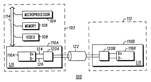
[0008] FIG. 1 is a block diagram of an exemplary computing system; and
[0009] FIG. 2 is a block diagram of an exemplary filter.
~~f'~;tlt '.
CA 02447404 2003-10-31
3
DETAILED DESCRIPTION OF THE DRAWINGS
[0010] The following detailed description of the invention is merely exemplary
in nature
and is not intended to limit the invention or the application and uses of the
invention.
Furthermore, there is no intention to be bound by any theory presented in the
preceding
background of the invention or the following detailed description of the
drawings.
[0011] According to various embodiments of the invention, a filter for an
input/output port
achieves improved electromagnetic filtering response by providing separate
current paths for
differential and single-ended signals. In one embodiment, a common mode choke
is
provided as a filter for relatively high-frequency differential signals.
Additionally, one or
more ferrites, inductors or other filter elements are provided in parallel to
the choke to filter
lower-frequency single-ended signals. By providing separate current paths for
the two types
of signals, the filter effectively passes both high and low-frequency signals
to the filter
output. Moreover, because the high-frequency filter is no longer required to
pass single-
ended signals, a choke with a higher attenuation than was previously possible
may be used,
thereby improving the overall effecti veness of the filter.
(0012] With reference now to FIG. 1, an exemplary computing system 100
suitably
includes a digital computer 102 that communicates with an external device 112
across
communications medium 122. In one embodiment, computer 102 is a personal
computer
and external device 112 is a peripheral device such as a digital camera,
printer, scanner,
input device, audiovisual device or the like. Computer 102 and external device
112 suitably
exchange data via medium 122 using any protocol or convention, such as USB
1.1, USB 2.0,
IEEE 1394, Ethernet, serial, parallel, or any other communications technique
presently
known or hereafter developed. Accordingly, various embodiments of
communications
medium 122 may encompass any type of cable, direct connection, wireless
connection,
cradle connection or the like.
[0013] Computer 102 is any processing device such as a personal computer,
workstation,
personal digital assistant, wireless phone, portable computer, video game
system or the like.
Computer 102 includes appropriate data processing components for the
particular
implementation, including a microprocessor 104, digital memory 106, optional
video card
108 and/or other components that communicate via a data bus 114 or other
interconnect as
appropriate. Computer 102 also includes an input/output (I/O) port 110A that
provides an
interface to communications medium 122 and to external device 112. Device 112
also
1-~C ~'t~'lt.~!
CA 02447404 2003-10-31
4
includes an appropriate input/output port 110B to support communications over
medium
122.
[0014] Each UO port 110A-B suitably includes a port controller 116 and a
filter 120. As
shown in Figure 1, elements 116A and 120A are associated with I/O port 110A,
and
elements 116B and 120B are associated with I/O port 110B. Although
implementations of
I/O ports 110A and 110B are described herein as being identical, the invention
is not so
limited. Indeed, in practice different devices 1021112 may include
implementations of I/O
ports 110 with widely varying components and architectures.
[0015] Port controller 116 is any circuit or component capable of transmitting
and
receiving data via communications medium 122. Port controller I16 also
communicates
with processor 104 or any other components in computer 102 via bus 114.
Accordingly, port
controller 116 may be implemented with any processor, digital signal processor
or controller
capable of converting data from bus 114 into a format that can be transported
by medium
122. Port controller 116 may be implemented as an application specific
integrated circuit
(ASIC), for example, that communicates with a transceiver (not shown) suited
for the
particular protocols transported on medium 122. In one embodiment, port
controller 116
includes a USB controller available from, for example, Motorola Inc.
[0016] In operation, port controller 116 converts data between protocols used
on bus 114
(e.g. the peripheral component interconnect (PCI) protocol) and those used on
media 122.
Many data protocols transmit data using "differential signals", which
generally encode data
based upon voltage differences between two transmitted electrical signals.
Differential
signals are generally less susceptible to noise than "single-ended signals"
that encode data
based upon voltage differences between a transmitted electrical signal and a
reference
voltage. Accordingly, port controller 116 typically supports two data signals
"D+" and "D-"
that are transmitted and received on two data lines 124 and 126, respectively,
across medium
122. To decode transmitted data, then, controller 116 suitably computes a
voltage difference
between signal "D+" received on signal line 124 and signal "D-" received on
signal line 126.
Many data protocols incorporate "combination signaling", which includes both
single-ended
and differential signals on signal lines 124 and 126. As an example, a
controller 116 for a
USB port 110 typically converts bus data to a differential signal represented
by differences
in voltages passed on signals D+ and D-. End of packet (EOP) indicators in the
USB
protocol are appropriately appended to the end of each data transmission as a
single-ended
iii, l ,~;g t
CA 02447404 2003-10-31
signal provided on either or both of signal lines D+ and D-, and other single-
ended signals
may also be present.
[0017] Filter 120 is any circuit or device capable of reducing or removing
noise,
electromagnetic interference (EMI) or other unwanted components of signals
transmitted or
received by I/O port 110. Filter 120 is suitably designed to attenuate
unwanted portions of
signals D+ and D- while having only minimal effects upon the signals
themselves. Because
the transmitted signals may contain both differential and single-ended
components, filter 120
suitably provides multiple current paths for the different types of signals,
as described more
fully below. In such embodiments, each of the paths contains a filtering
element appropriate
for removing EMI and/or noise from either a high or low frequency signal
corresponding to
a differential or single-ended signal, respectively. Accordingly, relatively
high-attenuation
filters can be provided for the differential signals, resulting in improved
EMI and/or noise
filtering.
[0018] With reference now to FIG. 2, an exemplary filter 120 suitably includes
a
differential mode signal path 202 and one or more single-ended signal paths
210, 212.
Single-ended paths 210, 212 are shown wired in parallel with differential path
202 so that
signals of varying frequencies and waveforms are appropriately filtered and
processed. Each
signal path 202, 210, 212 includes an appropriate filtering element 208, 204,
206
(respectively) such as an inductor, choke, fernte or the like that is selected
to remove EMI
andlor noise from signals D+ andlor D- without degrading the quality of the
signals
themselves. In an exemplary embodiment, differential mode current path 202
suitably
includes a relatively broad-spectrum filtering element 208, whereas single-
ended current
paths 210, 212 contain filtering elements 204, 206 that are tuned to pass
relatively low
frequency signals. Accordingly, EMI and other noise from signal lines 124, 126
can be
effectively reduced while both differential and single-ended signals are
effectively passed
through I/O port 110 (Figure 1 ).
[0019] FIG. 2 shows current paths 202, 210 and 212 as variously connecting
input
terminals 214 and 216, respectively, to output terminals 218 and 220,
respectively.
"Terminal" as used herein refers to any electrical node whatsoever, and may or
may not
include an interface for external connection or monitoring. Accordingly, while
the
discussion of input terminals 214, 216 and output terminals 218, 220 is
presented herein for
conceptualization and ease of explanation, each of these nodes are intended as
logical
concepts. In a practical embodiment, input terminals 214 and 216 may represent
any point
SS: f ~, ~~...i~~i~ 1..1 '. ..'
CA 02447404 2003-10-31
6
or node on signal lines 124 and 126 on the input side of filter 120, and
output terminals 218
and 220 may represent any point or node on signal lines 124 and 126 on the
output side of
filter 120. Each of these "terminals" may be physically indistinguishable from
other points
on signal lines 124 and 126, as appropriate. Moreover, many embodiments of
filter 120 are
intended as bi-directional filters. Accordingly, terminals 214 and 216 may
function as input
terminals while data is being transmitted and as output terminals when data is
being
received. Similarly, terminals 218 and 220 may function as both input and
output terminals,
depending on whether the particular I/O port 110 is transmitting or receiving
data.
[0020] Differential signal path 202 is any current path or set of paths that
is capable of
transmitting differential electrical signals. Differential signal path 202 is
typically
implemented using multiple signal paths (e.g. wires or other carriers) such
that each
component of the differential signal may be simultaneously passed to the
receiver. For USB
2.0 links, for example, a differential "1" logic state is denoted by the D+
signal line voltage
remaining at least 200 millivolts above the D- signal voltage. Similarly, a
differential "0"
logic state is denoted by the D+ signal voltage remaining at least 200
millivolts below the D-
signal voltage. Differential signals may be provided at a relatively high data
rate, and may
therefore require a relatively large amount of bandwidth. In a USB version 2.0
embodiment,
for example, the differential signals may be transmitted at a data rate on the
order of 480
million bits per second. Differential signal path 202 therefore includes a
differential mode
filter 208 that is capable of passing a relatively broad spectrum of
differential signals such as
a common mode choke. In one embodiment suitable for use with USB version 2.0
protocols, differential mode filter 208 is implemented with a model
DLW31SN222SQ2
common mode choke available from the Murata Manufacturing Co. of Kyoto, Japan.
While
this particular choke is a relatively high attenuation component with
impedance on the order
of about 2.2 kOhms at 100MHz, other models of chokes or other filtering
components
having a wide range of specifications could be used to implement other
embodiments of
filtering element 208.
[0021) Single-ended signal paths 210 and 212 are any current paths or sets of
paths that are
capable of transmitting single-ended electrical signals. Each single-ended
signal path 210,
212 is typically implemented using a single carrier, since the transmitted
signal is intended to
be compared to a reference signal available at the receiver. As shown in
Figure 2, single-
ended paths 210 and 212 are configured in parallel connection to differential
path 202 for
n.
~ .1 '-C ~ (! ~-'v ; "'
CA 02447404 2003-10-31
7
each signal line 124 and 126, respectively. In alternate embodiments, only one
single-ended
signal line 124 or 126 may be required.
[0022] According to most protocols with combination signaling, single-ended
signals are
commonly provided at much lower data rates than differential signals, and
therefore require
a relatively low amount of bandwidth. In a conventional USB implementation,
for example,
an end-of-packet (EOP) condition may be represented with a single-ended zero
(SEO) signal
that is out-of-band and asynchronous to the in-band differential signaling
discussed above.
The bandwidth requirements of single-ended filtering elements 204, 206, then,
are
correspondingly lower than those for differential filtering element 208. In
one embodiment
suitable for use with USB version 2.0 protocols, filtering elements 204, 206
are implemented
with ferntes or other filters commonly used with USB version 1.1
implementations, such as
the model BLM15BD601 ferrite available from Murata Manufacturing Co. Of course
other
models of ferrites, inductors or other filters having a wide range of
specifications could be
used to implement other embodiments of filtering elements 204 and 206.
[0023] In operation, then, filter 120 processes differential and single-ended
signals
received at input terminals 214 and 216 along separate paths to output
terminals 218, 220.
In-band differential signals are appropriately provided to a common-mode choke
or other
differential filter 208, which suitably reduces or removes EMI and/or noise
produced by
signal lines 124, 126 and/or other sources. Single-ended signals are
simultaneously provided
to one or more ferrites or other single-ended filters provided in parallel to
the differential
filter. Accordingly, both differential and single-ended signals are
effectively passed through
filter 120 without significant degradation or distortion.
[0024] By providing separate signal paths for the different types of signals,
greater noise
and EMI suppression can be applied to the differential signal. Generally
speaking, the terms
"high-attenuation" and "broad spectrum" filter as used herein refer to filters
with impedance
in excess of about 150-200 ohms, and possibly as high as about 3 kOhms or even
higher.
"Low attenuation" filters, as described herein, typically exhibit impedances
of about 90
ohms as commonly used in many prior art implementations of USB version 2Ø As
briefly
mentioned above, broad spectrum filtering was not previously available for
filtering
combination signals because the high attenuation tended to distort the single-
ended
waveforms passing through the filter. By providing separate paths 210 and 212
for single-
ended signals, then, the attenuation of the in-band path 202 can be greatly
increased, thus
~~~ ~1°;1~'..'
CA 02447404 2003-10-31
resulting in greatly improved EMI and/or noise reduction in filter 120 and
improved
performance in Il0 port 110.
[0025] While an exemplary embodiments) has been presented in the foregoing
detailed
description of the invention, it should be appreciated that a vast number of
variations and
equivalents exist. For example, while certain aspects of the invention have
been described
herein with reference to the universal serial bus standard, the concepts
disclosed herein may
be readily adapted to other port or interface specifications such as SCSI,
wireless, or any
other protocol that incorporates combination signaling. It should be
appreciated that these
exemplary embodiments are only examples, and are not intended to limit the
scope,
applicability, or configuration of the invention in any way. Rather, the
foregoing detailed
description will provide a convenient road map for implementing exemplary
embodiments of
the invention. Various changes may be made in the function and arrangement of
elements
described in any of the exemplary embodiments without departing from the scope
of the
invention as set forth in the appended claims and their legal equivalents.