Note: Descriptions are shown in the official language in which they were submitted.
CA 02447882 2003-11-17
WO 02/096655 PCT/US02/16507
ROBUST BIT SCHEME FOR A MEMORY
OF A REPLACEABLE PRINTER COMPONENT
The Field of the Invention
The present invention relates to printers and to memories for printers.
More particularly, the invention relates to a robust bit scheme for a memory
of a
replaceable printer component.
Background of the Invention
The art of inkjet technology is relatively well developed. Commercial
products such as computer printers, graphics plotters, and facsimile machines
have been implemented with inkjet technology for producing printed media.
Generally, an inkjet image is formed pursuant to precise placement on a print
medium of ink drops emitted by an ink drop generating device known as an
inkjet printhead assembly. An inkjet printhead assembly includes at least one
printhead. Typically, an inkjet printhead assembly is supported on a movable
carriage that traverses over the surface of the print medium and is controlled
to
eject drops of ink at appropriate times pursuant to command of a microcomputer
or other controller, wherein the timing of the application of the ink drops is
intended to correspond to a pattern of pixels of the image being printed.
Inkjet printers have at least one ink supply. An ink supply includes an
ink container having an ink reservoir. The ink supply can be housed together
with the inkjet printhead assembly in an inkjet cartridge or pen, or can be
housed
separately. When the ink supply is housed separately from the inkjet printhead
assembly, users can replace the ink supply without replacing the inkjet
printhead
assembly. The inkjet printhead assembly is then replaced at or near the end of
the printhead life, and not when the ink supply is replaced.
1
CA 02447882 2003-11-17
WO 02/096655 PCT/US02/16507
Current printer systems typically include one or more replaceable printer
components, including inkjet cartridges, inkjet printhead assemblies, and ink
supplies. Some existing systems provide these replaceable printer components
with on-board memory to communicate information to a printer about the
replaceable component. The on-board memory, for an inkjet cartridge for
example, may store information such as pen type, unique pen code, ink fill
level,
marketing information, as well as other information. Such a memory may also
store other information about the ink container, such as current ink level
information. The ink level information can be transmitted to the printer to
indicate the amount of ink remaining. A user can observe the ink level
information and anticipate the need for replacing a depleted ink container.
If the data received by a printer from a printer component memory
contains an error, the printer may perform an incorrect action, or may be
unable
to use the printer component. Such an error may be the result of a short
circuit
or open circuit in an address line coupling the memory to other printer
components, such as a printer controller, or from some other problem.
It is desirable to have a memory scheme that is more robust than current
memory schemes used in replaceable printer components to detect and correct
errors and provide uninterrupted operation.
Summary of the Invention
The present invention provides a method for detecting an error in data
received from a memory of a replaceable printer component. The memory
includes a plurality of bits. The method includes providing a first parity bit
associated with a first data item. The first data item and the first parity
bit are
stored in the printer memory. The printer includes a plurality of electrically
conductive lines. At least one of the electrically conductive lines is
associated
with each bit. The first data item and the first parity bit are read from the
memory. An electrical test of at least one of the electrically conductive
lines is
performed. An error in the first data item is identified based on the first
parity
bit read from the memory and the electrical test.
One aspect of the invention is directed to a printing system including an
inkjet printhead for selectively depositing ink drops on print media. An ink
2
CA 02447882 2008-01-30
supply stores ink to be provided to the inkjet printhead. A memory device
stores
a first parity bit and a first data item. The first parity bit is associated
with the
first data item. A processor is coupled to the memory device by a plurality of
electrically conductive lines. The processor is responsive to output of the
memory device. The processor performs an electrical test of at least one of
the
electrically conductive lines. The processor identifies an error in the first
data
item based on the first parity bit and the electrical test.
Another aspect of the invention is directed to a replaceable printer
component for a printing system having a controller. The printer component
comprises an information storage device that stores a first parity bit and a
first
data item. The first parity bit is associated with the first data item. The
first
parity bit is used by the controller in conjunction with an electrical test of
electrically conductive lines coupled to the information storage device to
identify
an error in the first data item.
Another aspect of the invention is directed to a memory for a replaceable
inkjet printer component of a printing system. The memory includes a
semiconductor die. A plurality of circuits are formed on the semiconductor
die.
Each circuit is associated with and determines the state of a bit in the
memory.
The memory stores a first data item, which provides identifying information
regarding the replaceable inkjet printer component. The first data item is
useable
by the printing system to determine whether the replaceable inkjet printer
component is appropriate for use in the printing system. The circuits
associated
with the first data item are positioned substantially near a center of the
semiconductor die.
Brief Description of the Drawings
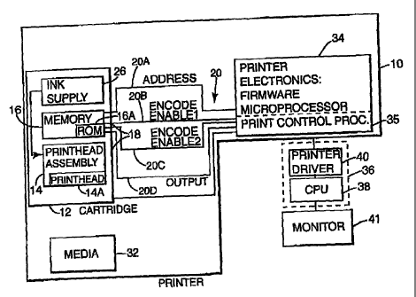
Figure 1 is an electrical block diagram of major components of an inkjet
printer according to the present invention.
Figure 2 is a diagram illustrating the ROM of the printer shown in
Figure 1.
3
CA 02447882 2003-11-17
WO 02/096655 PCT/US02/16507
Figure 3 is a table illustrating information stored in an inkjet cartridge
memory according to the present invention.
Figure 4A is a schematic diagram of a circuit for defining the state of a
fusible bit of an inkjet cartridge memory of the present invention.
Figure 4B is a schematic diagram of a circuit for defining the state of a
masked bit of an inkjet cartridge memory of the present invention.
Figure 5A is a table illustrating two examples of bit assignments in an
inkjet cartridge memory according to the present invention.
Figure 5B is a table illustrating the bit assignments of Figure 5A after an
error has occurred.
Description of the Preferred Embodiments
In the following detailed description of the preferred embodiments,
reference is made to the accompanying drawings that form a part hereof, and in
which is shown by way of illustration specific embodiments in which the
invention may be practiced. It is to be understood that other embodiments may
be utilized and structural or logical changes may be made without departing
from the scope of the present invention. The following detailed description,
therefore, is not to be taken in a limiting sense, and the scope of the
present
invention is defined by the appended claims.
Figure 1 is an electrical block diagram of major components of an inkjet
printer according to the present invention. Inkjet printer 10 includes
removable
inkjet cartridge 12, which includes an inkjet printhead assembly 14, an
integrally
mounted memory 16, and an ink supply 26. Inkjet cartridge 12 is pluggably
removable from printer 10 via interconnects 18. Inkjet printhead assembly 14
includes at least one printhead 14A. Memory 16 may include multiple forms of
memory, including RAM, ROM and EEPROM, and stores data associated with
inkjet printhead assembly 14 and ink supply 26. In one embodiment, memory
16 includes factory-written data and printer-recorded data. In one embodiment,
memory 16 includes a 26-bit ROM 16A, having 13 fusible bits, and 13 masked
bits. In an alternative embodiment, all 26 bits are fusible bits. In another
form
of the present invention, all 26 bits are masked bits. ROM 16A can also
include
a different number of total bits, other than 26 bits. An advantage of using
both
4
CA 02447882 2003-11-17
WO 02/096655 PCT/US02/16507
fusible and masked bits is that a size reduction in ROM 16A may be obtained.
Each fusible bit may be set by blowing a resistor in a circuit 400A (shown in
Figure 4A) representing the fusible bit. Each masked bit may be set by adding
a
resistor in a circuit 400B (shown in Figure 4B) representing the masked bit.
In
one embodiment, ROM 16A is integrated with inkjet printhead assembly 14. In
an alternative embodiment, ROM 16A may be integrated with ink supply 26. It
will be understood by one of ordinary skill in the art that, rather than
incorporating inkjet printhead assembly 14 and ink supply 26 into an inkjet
cartridge 12, inkjet printhead assembly 14 and ink supply 26 may be separately
housed and may include separate memories.
Printer 10 includes communication lines 20 for communications between
inkjet cartridge 12 and controller 34. Communication lines 20 specifically
include address lines 20A, first encode enable line 20B, second encode enable
line 20C, and output line 20D, which are all connected to ROM 16A. In one
embodiment, address lines 20A include 13 address lines. First encode enable
line 20B is used to select fusible bits in ROM 16A, and second encode enable
line 20C is used to select masked bits in ROM 16A. Address lines 20A are used
to select a particular fusible bit or masked bit. The value of a selected
fusible or
masked bit is read by sensing the output on output line 20D.
Inkjet printhead assembly 14, memory 16, and ink supply 26 are
connected to controller 34, which includes both electronics and firmware for
the
control of the various printer components or sub-assemblies. A print control
procedure 35, which may be incorporated in the printer driver, causes the
reading of data from memory 16 and adjusts printer operation in accordance
with
the data accessed from memory 16. Controller 34 controls inkjet printhead
assembly 14 and ink supply 26 to cause ink droplets to be ejected in a
controlled
fashion on print media 32.
A host processor 36 is connected to controller 34, and includes a central
processing unit (CPU) 38 and a software printer driver 40. A monitor 41 is
connected to host processor 36, and is used to display various messages that
are
indicative of the state of inkjet printer 10. Alternatively, printer 10 can be
configured for stand-alone or networked operation wherein messages are
displayed on a front panel of the printer.
5
CA 02447882 2003-11-17
WO 02/096655 PCT/US02/16507
Figure 2 is a diagram illustrating ROM 16A of Figure 1 in additional
detail. ROM 16A includes semiconductor die 60 having a plurality of pads 62.
Address lines 20A, first encode enable line (El) 20B, second encode enable
line
(E2) 20C, and output line 20D are coupled to semiconductor die 60 via pads 62.
Address lines 20A include 13 address lines (A1-A13). In one embodiment,
ROM 16A includes other electrical connections (not shown), including ground
connections.
Figure 3 is a table illustrating information stored in ROM 16A according
to the present invention. Table 300 includes address line identifiers 302,
encode
enable line identifiers 304, bit type identifiers 306A and 306B (collectively
referred to as bit type identifiers 306), bit values 308, and fields 310.
Table 300
is divided into portion 312 and portion 314. Portion 312 of table 300
represents
information associated with fusible bits, as indicated by fusible type
identifier
306A. Portion 314 of table 300 represents information associated with masked
bits, as indicated by masked type identifier 306B. As mentioned above, rather
than using both fusible and masked bits, all bits in ROM 16A may be fusible
bits, or all bits in ROM 16A may be masked bits. Each one of the address line
identifiers 302 represents one of address lines 20A, and corresponds to either
a
fusible bit or a masked bit. Both the fusible and the masked bits are numbered
1-
13, indicating the particular address line 20A associated with the bit. Encode
enable line identifiers 304 indicate the encode enable line 20B or 20C that
must
be set in order to select the corresponding bit. A"1" in encode enable line
identifiers 304 corresponds to first encode enable line 20B, which is used to
select fusible bits. A"2" in encode enable line identifiers 304 corresponds to
second encode enable line 20C, which is used to select masked bits.
Fusible bits 1-13 and masked bits 1-13 are divided into a plurality of
fields 310. Each bit in a particular field 310 includes a bit value 308. When
a
bit is set, it has the value indicated in its corresponding bit value 308.
When a
bit is not set, it has a value of 0. In one embodiment, fusible bits 1-13 and
masked bits 1-13 are set during manufacture of ROM 16A.
Field 310A includes fusible bit 13. In one embodiment, fusible bit 13 is
not used to store data, so field 310A includes the letters "NA" (i.e., not
assigned).
6
CA 02447882 2003-11-17
WO 02/096655 PCT/US02/16507
Ink fill field 310B includes fusible bits 10-12. In one embodiment,
fusible bits 10-12 provide a reference level or trigger level to determine
when a
low ink warning should be displayed.
Parity field 310C includes fusible bit 9. In one embodiment, fusible bit 9
is a parity bit used in association with the bits corresponding to marketing
field
310D. In an alternative embodiment, fusible bit 9 is a parity bit used in
association with multiple ones of the fields 310. Fusible bit 9 may also be
used
in association with memory bits associated with another printer component,
such
as ink supply 26.
Marketing field 310D includes fusible bits 6-8. In one embodiment,
fusible bits 6-8 are used to identify whether an inkjet cartridge can be used
in a
particular printer.
Field 310E includes fusible bit 5. In one embodiment, fusible bit 5 is not
used to store data, so field 310E includes the letters "NA" (i.e., not
assigned).
Pen uniqueness field 310F includes fusible bits 2-4. In one embodiment,
fusible bits 2-4 represent a random number that uniquely identifies an inkjet
cartridge, which allows printer controller 34 to determine when a new inkjet
cartridge has been installed.
Field 310G includes fusible bit 1. In one embodiment, fusible bit 1 is not
used to store data, so field 310G includes the letters "NA" (i.e., not
assigned).
Field 310H includes masked bits 10-13. In one embodiment, masked bits
10-13 are not used to store data, so field 310H includes the letters "NA"
(i.e., not
assigned).
Field 3101 includes masked bit 9. In one embodiment, masked bit 9 is a
parity bit used in association with the bits corresponding to pen type field
310J.
In an alternative embodiment, masked bit 9 is a parity bit used in association
with multiple ones of the fields 310. Masked bit 9 may also be used in
association with memory bits associated with another printer component, such
as
ink supply 26.
Pen type field 310J includes masked bits 5-8. In one embodiment,
masked bits 5-8 provide an identification of the type of inkjet cartridge that
is
associated with the memory.
Pen uniqueness field 310K includes masked bits 1-4. In one
embodiment, masked bits 1-4 represent a random number that uniquely identifies
7
CA 02447882 2003-11-17
WO 02/096655 PCT/US02/16507
a particular inkjet cartridge, which allows printer controller 34 to determine
when a new inkjet cartridge has been installed.
Figure 4A is a schematic diagram of a circuit for defining the state of a
fusible bit in ROM 16A. Circuit 400A includes first encode enable input (E_on)
402, output (id_out) 404, address input 406, transistor 408, resistor 410,
transistor 412, second encode enable input (E_off) 414, transistor 416, and
ground (p_gnd) 418. Address input 406 is coupled to one of address lines 20A
(shown in Figure 1). First encode enable input 402 is coupled to first encode
enable line 20B (shown in Figure 1). Second encode enable input 414 is coupled
to second encode enable line 20C (shown in Figure 1). Output 404 is coupled to
output line 20D (shown in Figure 1).
In one embodiment, each of transistors 408, 412 and 416 is a field effect
transistor (FET). Address input 406 is coupled to the drain of transistor 408.
First encode enable input 402 is coupled to the gate of transistor 408. The
source of transistor 408 is coupled to the gate of transistor 412 and the
drain of
transistor 416. The gate of transistor 416 is coupled to second encode enable
input 414. The drain of transistor 416 is coupled to the source of transistor
408
and the gate of transistor 412. The source of transistor 416 is coupled to
ground
418. Resistor 410 is positioned between output 404 and the drain of transistor
412. The source of transistor 412 is coupled to ground 418.
A fusible bit in ROM 16A, such as the bit represented by circuit 400A, is
read by setting first encode enable input 402 high, setting address input 406
high, and sensing the signal at output 404. First encode enable input 402 is
set
high by controller 34 by setting first encode enable line 20B high. Address
input
406 is set high by controller 34 by setting the address line 20A coupled to
address input 406 high. The output voltage at output 404 is sensed by
controller
34 by sensing the voltage on output line 20D.
Transistor 408 acts as an AND gate, with inputs 402 and 406. If inputs
402 and 406 are both high, a current flows through transistor 408, turning on
transistor 412. Transistor 412 acts as a drive transistor, driving output 404.
If
resistor 410 is blown, the voltage at output 404 will be high, indicating a
logical
1. If resistor 410 is not blown, the voltage at output 404 will be low,
indicating a
logical 0. Transistor 416 is used as an active pull down to prevent leakage
current from transistor 408 from turning on transistor 412 when transistor 412
8
CA 02447882 2003-11-17
WO 02/096655 PCT/US02/16507
should be off. Transistor 416 is turned on by setting second encode enable
input
414 high. When turned on, transistor 416 diverts current from transistor 408
to
ground.
In one embodiment, transistors 408 and 416 each have a length of about
4 micrometers and a width of about 15.5 micrometers, and transistor 412 has a
length of about 4 micrometers and a width of about 600 micrometers. In one
embodiment, resistor 410 has a resistance of over about 1000 ohms when blown,
and a resistance of under about 400 ohms when not blown. In addition to
blowing resistor 410, other methods may be used to create an open circuit to
define the state of a bit in ROM 16A, including mechanical cutting, laser
cutting,
as well as other methods.
Figure 4B is a schematic diagram of a circuit for defining the state of a
masked bit in ROM 16A. Circuit 400B is substantially the same as circuit 400A
shown in Figure 4A, with the exceptions that resistor 410 is replaced by
switch
420, and transistor 422 includes different properties than transistor 412. In
one
embodiment, switch 420 is not an actual physical switch, but represents either
the presence or absence of a resistor. If a resistor is present in place of
switch
420, the resistor has sufficient resistance to act as an open circuit between
output
404 and transistor 422. If a resistor is not present in place of switch 420,
there is
no additional resistance between output 404 and transistor 422. In one
embodiment, transistor 422 is a field effect transistor (FET), with a length
of
about 4 micrometers and a width of about 100 micrometers.
Address input 406 is coupled to one of address lines 20A (shown in
Figure 1). First encode enable input 402 is coupled to second encode enable
line
20C (shown in Figure 1). Second encode enable input 414 is coupled to first
encode enable line 20B (shown in Figure 1). Output 404 is coupled to output
line 20D (shown in Figure 1).
Address input 406 is coupled to the drain of transistor 408. First encode
enable input 402 is coupled to the gate of transistor 408. The source of
transistor
408 is coupled to the gate of transistor 422 and the drain of transistor 416.
The
gate of transistor 416 is coupled to second encode enable input 414. The drain
of transistor 416 is coupled to the source of transistor 408 and the gate of
transistor 422. The source of transistor 416 is coupled to ground 418. Switch
9
CA 02447882 2003-11-17
WO 02/096655 PCT/US02/16507
420 is positioned between output 404 and the drain of transistor 422. The
source
of transistor 422 is coupled to ground 418.
A masked bit in ROM 16A, such as the bit represented by circuit 400B,
is read by setting first encode enable input 402 high, setting address input
406
high, and sensing the signal at output 404. First encode enable input 402 is
set
high by controller 34 by setting second encode enable line 20C high. Address
input 406 is set high by controller 34 by setting the address line 20A coupled
to
address input 406 high. The output voltage at output 404 is sensed by
controller
34 by sensing the voltage on output line 20D.
Transistor 408 acts as an AND gate, with inputs 402 and 406. If inputs
402 and 406 are both high, a current flows through transistor 408, turning on
transistor 422. Transistor 422 acts as a drive transistor, driving output 404.
If
switch 420 is open (i.e., resistor present), the voltage at output 404 will be
high,
indicating a logical 1. If switch 420 is closed (i.e., resistor not present),
the
voltage at output 404 will be low, indicating a logical 0. Transistor 416 is
used
as an active pull down to prevent leakage current from transistor 408 from
turning on transistor 422 when transistor 422 should be off. Transistor 416 is
turned on by setting second encode enable input 414 high. When turned on,
transistor 416 diverts current from transistor 408 to ground.
In ROM 16A of the present invention, fusible and masked bits may be
further classified as either functional or informational. Functional bit
fields must
match values expected by the printer for proper operation. An example of a
functional bit field is pen type field 310J. If the bits corresponding to pen
type
field 310J indicate a type of inkjet cartridge that is not compatible with the
printer, the printer may disable the inkjet cartridge. Thus, an error in pen
type
field 310J could cause the printer to improperly disable an inkjet cartridge.
Informational bit fields are not critical to proper operation and may be
ignored,
or action may be taken based on incorrect information in an informational bit
field without causing a stoppage in operation. Examples of informational bit
fields include pen uniqueness fields 310F and 310K.
Short circuits caused by stray ink ("ink shorts") in an inkjet cartridge
ROM 16A typically occur more frequently toward the edges of the
semiconductor die 60 (shown in Figure 2). Pads 62 that are positioned near the
edges of semiconductor die 60 tend to suffer from corrosion, potentially
causing
CA 02447882 2003-11-17
WO 02/096655 PCT/US02/16507
electrical failures. In one embodiment, functional bits and other important
bits,
such as parity bits, are positioned toward the center of semiconductor die 60
to
reduce the likelihood of ink shorts with respect to these bits, and thereby
provide
a more robust ROM 16A. In one embodiment, marketing bits 310D, pen type
bits 310J, and parity bits 310C and 3101 are positioned substantially near the
center of semiconductor die 60.
In one embodiment, to further improve the robustness of an inkjet
cartridge ROM 16A according to the present invention, parity bits are assigned
to important bit fields, including functional bit fields. As shown in Figure
3, a
parity bit 310C is assigned to marketing bit field 310D, and a parity bit 3
101 is
assigned to pen type bit field 310J. The use of parity bits, such as parity
bits
310C and 3 101, to improve the robustness of an inkjet cartridge ROM, is
discussed in further detail below with reference to figures 5A and 5B.
Figure 5A is a table illustrating two examples of bit assignments in an
inkjet cartridge ROM according to the present invention. The table includes
lines 502 and 504, and columns 506 and 508A-D. Column 506 includes the
value of a parity bit for each example, such as parity bit 310C or 3101.
Columns
508A-D include the value of bits in a data bit field for each example, such as
marketing field 310D or pen type field 310J. In Example 1, shown on line 502,
the parity bit is set to 0, bit 1 is set to 0, bit 2 is set to 0, bit 3 is set
to 1, and bit 4
is set to 1. In Example 2, shown on line 504, the parity bit is set to 1, bit
1 is set
to 1, bit 2 is set to 0, bit 3 is set to 0, and bit 4 is set to 0.
In one embodiment, even parity is used in determining what value to
assign to the parity bits. Since bits 1-4 in Example 1 add up to an even
number,
the parity bit for Example 1 is set to 0 to maintain an even number for the
sum of
bits 1-4 and the parity bit. Since bits 1-4 in Example 2 add up to an odd
number,
the parity bit for Example 2 is set to 1 to produce an even number for the sum
of
bits 1-4 and the parity bit. In an alternative embodiment, odd parity is used
rather than even parity.
Figure 5B is a table illustrating the bit assignments of Figure 5A after an
error in the data bit fields has occurred. It is assumed in Figure 5B that an
ink
short has occurred in the address line 20A corresponding to data bit 3.
Controller 34 determines whether any of address lines 20A has a short circuit
or
open circuit by electrically testing each of address lines 20A. In one
11
CA 02447882 2003-11-17
WO 02/096655 PCT/US02/16507
embodiment, the electrical test includes a check for continuity. Techniques
for
testing electrically conductive lines and electric circuits are known to those
of
ordinary skill in the art. After electrically testing address lines 20A,
controller
34 determines that the address line 20A corresponding to bit 3 has a short.
When an ink short occurs in an address line, the output read by controller 34
will
be a 1, regardless of whether the bit was a 1 prior to the ink short. Thus,
bit 3 is
a 1 for both Example 1 and Example 2 in Figure 5B, even though bit 3 in
Example 2 should be a 0 as shown in Figure 5A.
In Example 1, controller 34 examines the parity bit to determine if the
data bit field contains an error. Since the sum of bits 1-4 and the parity bit
is an
even number, controller 34 determines that the data bit field does not contain
an
error.
In Example 2, after examining the parity bit to determine if the data bit
field contains an error, controller 34 determines that an error occurred,
since the
sum of bits 1-4 and the parity bit is an odd number, and even parity is being
used. Based on the electrical test of the address line corresponding to bit 3,
which indicated an ink short, and the determination from the parity test that
an
error occurred, controller 34 determines that bit 3 should be a 0, and
corrects the
bit accordingly. Thus, the error does not cause an interruption in the
operation
of printer 10.
Although specific embodiments have been illustrated and described
herein for purposes of description of the preferred embodiment, it will be
appreciated by those of ordinary skill in the art that a wide variety of
alternate
and/or equivalent implementations may be substituted for the specific
embodiments shown and described without departing from the scope of the
present invention. Those with skill in the chemical, mechanical, electro-
mechanical, electrical, and computer arts will readily appreciate that the
present
invention may be implemented in a very wide variety of embodiments. This
application is intended to cover any adaptations or variations of the
preferred
embodiments discussed herein. Therefore, it is manifestly intended that this
invention be limited only by the claims and the equivalents thereof.
12