Note: Descriptions are shown in the official language in which they were submitted.
CA 02448012 2003-11-21
WO 02/101854 PCT/US02/08217
COATING EDGE CONTROL
Field of the Invention
The invention relates to coating methods that include techniques of
controlling
edge thickness and profile, and products prepared from those methods.
Background
Coated webs are used in a multitude of commercial and consumer products. A
single example is batteries, some of which are constructed from a web coated
with a
conductive material and wound into a roll or stacked into a number of
laminated layers.
See, e.g., United States Patent Number 5,360,684, among others.
Films coated onto webs often suffer from different thickness across the width
of
the film, especially at the coated film edge. If no effort is made to control
the thickness or
cross-sectional profile of the edge, an edge of a coated material will
generally taper off in
a gradual slope from the thickness of the bulk coating, to zero thickness.
Undesirable results of a tapered edge will result with the particular effect
being
dependent on the application that the coated material is designed for. In
batteries
constructed of multiple wound or stacked layers, undesirable possibilities of
an uneven or
tapered edge result upon placing the coated substrates into a layered
configuration. An
"edge effect" can result because the capacity of the tapered edge of a coated
cathode is
used up faster than the capacity of the bulk coating. This edge effect results
in a non-
uniform charge density, may cause hot-spots or shorts in the battery, and can
ultimately
result in a reduced cycle life.
Methods of"attempting to control edge thicknesses and profiles are various,
some
including the use of dams or air or water systems designed to remove a coated
film layer
from a coated substrate.
Summary of the Invention
The invention involves methods of applying a coating material onto a
substrate,
especially where the edge of the coating material has a desirable shape or
thickness
profile.
1
CA 02448012 2003-11-21
WO 02/101854 PCT/US02/08217
The term "thickness profile" refers to the thickness, as viewed from the side
(i.e., a
cross-section directed along the machine direction) of materials coated on a
surface of a
substrate, and is used herein to reference coating thickness at a coating
material edge. The
thickness profile of coatings of a coating material edge partially or
completely coated over
with edge material is based on the total thickness of the coating material and
the edge
material. Where only the coating material is coated on an area of a substrate,
the thickness
profile is taken as the thickness of the coating material alone.
An "improved thickness profile" is a thickness profile that provides some
improvement or advantage relative to a thickness profile that is produced
without using an
edge material in a manner described herein. Preferably, the invention allows a
thickness
that is relatively uniform at the edge of a coated coating material. Examples
of improved
thickness profiles include the thicluiess profiles of coating material edges
shown in figures
la, 5 and 10.
Improved thickness profiles at an edge of a coated coating material can be
produced using an edge material coated adjacent to and in contact with the
coating
material. The edge material may augment or coat over the edge of the coating
material to
provide a uniform total thickness of materials along the coating material
edge.
Alternatively, with some of the coating techniques described herein, the edge
material may
affect the actual shape of the coating material edge, causing the edge of the
coating
material itself to form an improved shape with a desirable thickness profile
(with or
without augmentation of the thickness using the edge material). Such an
"improved edge"
can be an edge that has an improved shape relative to a typical, relatively
wide taper
produced without the use of an edge material, especially an edge having a more
narrow
width or a steeper slope relative to an edge of a coating material coated
without the use of
an edge material.
The edge material may be coated prior to the coating material, the coating
material
may be coated prior to the edge material, or the two materials may be coated
substantially
simultaneously or simultaneously.
In one embodiment of the invention, a coating material coated on a substrate
exhibits a tapered edge. According to the invention, edge material is coated
to contact the
edge of the coating material to augment the thickness at the coating material
edge and
produce a desired thickness profile at the edge based on the combined
thicluiess of the
2
CA 02448012 2003-11-21
WO 02/101854 PCT/US02/08217
coating material and the edge material. Advantages result from the uniform
thickness
profile, e.g., a thickness profile that is uniform to within 10%, or 5%
variation. For
instance, when the coated substrate is wound, it winds evenly in the region of
the coating
material edge as opposed to uneven winding if the edge has an uneven thickness
profile.
In another embodiment, an edge material can be used as a physical boundary
against which coating material is coated, to form a desired coating material
edge and a
desired thickness profile at the coating material edge. The edge material and
the barrier
material are preferably immiscible. The result can be an improved thickness
profile at the
edge of the coating material, including an improved shape of the coating
material edge.
This embodiment can also improve winding of the coated material in the region
of the
coating material edge, due to an improved thicluiess profile. This embodiment
not only
covers up a tapered coating material edge, but can in fact work to improve the
shape of the
edge and the thickness profile at the edge of the coating material itself.
Covering up coating material edge causes the covered coating material to
become
non-functional and essentially wasted. Ideal coating techniques would allow a
coated
edge of a coating material to contact a coated edge of an edge material, with
the two edges
taking the form of square edges at their interface which do not taper or
overlap. (See, e.g.,
figure 4.) Or, it can also be useful to simply reduce the amount of coating
material that
ends up constituting an edge, e.g., by increasing the slope and decreasing the
width of the
tapered edge and thereby reducing the amount of coating material wasted as the
edge.
(See, e.g., figure 5.) According to certain embodiments of the inventive
method, coating
conditions and edge materials and coating materials can be chosen to result in
a coating
material edge that is less tapered as measured by the slope of the tapered
edge. The more
steep the coating material edge, the less coating material is wasted, so steep
coating
material edges can be preferred.
When used to prepare products having a wound or stacked construction, the
method of the invention can allow for coating processes that give a uniform
thickness
profile at the edge of the coating material. This can give manufacturing
efficiencies
relative to winding the substrate with an uneven edge or relative to other
methods of
dealing with the uneven edge. Compare, for example, United States Patent
Number
5,360,684, which describes methods of preparing stacked battery constructions.
3
CA 02448012 2003-11-21
WO 02/101854 PCT/US02/08217
In a specific application of the invention, the coating material can be a
cathode
material. The edge material can be used to improve the shape of the cathode
material edge
or to cover a tapered cathode material edge, leveling the overall thickness of
the coated
materials at the cathode material edge and facilitating winding or stacking to
form a
product with desired edge properties. The edge material can optionally and
preferably be
chosen to perform a desired function in the wound or stacked product
construction, such as
a barrier to moisture, water, or light, and can also optionally and preferably
be an
insulating material.
A specific embodiment of a battery component produced using the method of the
invention can have a cathode material edge in contact with an insulating edge
material.
The insulating edge can act as a barrier to light, water, or other debris,
etc. Alternatively
or in combination, the insulating edge material can prevent the free edge of a
current
collector or anode from contacting a different component of a stack,
potentially causing a
short circuit. The insulating edge material serves the purpose of insulating
components of
the battery product, and is very adaptable to high-speed manufacturing.
Insulating
components of the stack from electrical contact can prevent undesired effects
such as
current density variations and shorts that might otherwise occur, e.g.,
following winding.
An aspect of the invention relates to a method of coating a substrate with a
cathode
material for an electrochemical cell. The method generally includes steps of
providing a
substrate, coating edge material onto the substrate, and coating cathode
material onto
the substrate. The coating material and the edge material contact each other,
and the
thickness profile at the edge of the coated cathode material is improved
relative to a
thickness profile of an edge of a cathode material coated without the edge
material.
Another aspect of the invention relates to a method of coating a substrate
with a
coating material. The method generally includes steps of providing a
substrate, coating
non-viscoelastic, polymer-containing, electrically insulating, edge material
onto the
substrate, and coating a coating material onto the substrate. The coating
material and edge
material contact each other, and the thickness profile of the coating material
edge can be
improved relative to a thickness profile of a coating material edge produced
without the
edge material.
Another aspect of the invention relates to a method of coating a substrate
with a
coating material. The method generally includes providing a substrate, coating
edge
4
CA 02448012 2003-11-21
WO 02/101854 PCT/US02/08217
material onto the substrate using a coater that is a slotted die coater and
that is not a
curtain coater, and using the same slotted die coater to coat a coating
material onto the
substrate. The edge material and the coating material contact each other, and
the thickness
profile of the coating material edge is improved relative to a thickness
profile of a coating
material edge produced without the edge material.
Yet another aspect of the invention relates to a method of preparing a battery
cathode. The method includes providing a substrate, using a slotted die coater
to coat a
cathode material onto the substrate, and from a second slot of the same die
coater, coating
edge material onto the substrate, wherein the coating material and the edge
material are in
contact at their respective edges.
Yet a further aspect of the invention relates to a method of coating a
substrate with
a cathode material for an electrochemical cell. The method includes providing
a substrate,
coating a cathode material onto the substrate, and coating an insulating edge
material onto
the substrate. The edge material acts as a barrier, and the coating material
and the edge
material contact each other. The insulating edge material can also act to
insulate layers of
a stacked battery component from each other, e.g., to insulate an anode from a
current
collector by preventing electrical contact between them.
Still a further aspect of the invention relates to a battery component that
includes
an anode, a separator having a surface adjacent to a surface of the anode, a
cathode having
a surface adjacent to another surface of the separator, an edge material
contacting an edge
of the cathode, and a current collector contacting the cathode. The edge
material acts as a
barrier material to protect the edge of the cathode.
Brief Description of the Drawings
Figure 1 is a side view illustration, in a machine direction, of a typical
coating of a
coating material, having a tapered edge.
Figure 1 a illustrates the coating material of figure 1 further coated with an
edge
material to at least partially cover the tapered edge.
Figures 2a and 2b are side-view illustrations of exemplary die coating
apparatuses
useful to die coat a coating material and an edge material according to the
invention.
Figure 3 is an end view of an exemplary die coating apparatus for use
according to
the methods of the invention.
5
CA 02448012 2003-11-21
WO 02/101854 PCT/US02/08217
Figure 4 is a side view illustration of a coating of coating material and edge
material coated to an improved, approximately or exactly square edge for each
material.
Figure 5 is a side view illustration of a coating of coating material and edge
material coated to an improved edge having a relatively steep slope and a
relatively
narrow width.
Figure 6 is a set of illustrations of an exemplary battery component.
Figure 7 illustrates a stripe-coated substrate.
Figure 8 illustrates another stripe-coated substrate.
Figure 9 illustrates a stacked battery component.
Figure 10 is a scanning electron micrograph of a cross section of one of the
coatings of example 1 illustrating the improved edge.
All of the figures are not shown to proper scale.
Detailed Description
In general, the invention involves applying, e.g., coating, materials onto a
substrate, including a coating material and an edge material, with the two
materials being
adjacent to and contacting each other. In some preferred embodiments of the
invention,
the coating methods can result in a desired thickness profile at the edge of
the coating
material, optionally including a desired shape of the coating material edge
effected by the
coating technique.
In comparison to a tapered thickness profile at the edge of a coated film
produced
by conventional coating methods, the invention can be used to augment the
thickness of
the tapered edge with an edge material, giving a thickness profile of the
combined
materials that facilitates subsequent processing and that can improve product
construction
or performance.
In certain embodiments, the invention allows a coating material and an edge
material to be coated in such a way that the edge material affects the shape
of the coating
material edge and improves the shape, especially to form a narrower (i.e.,
less wide) edge
with a steeper taper, and ideally to approximate or actually produce a square
coating
material edge. Accordingly, a desired thickness profile of the coating
material edge can be
formed by using the edge material as a physical boundary that contacts the
coating
material to form a coating material edge having a desirable shape and
thickness profile,
6
CA 02448012 2009-08-25
60557-7033
most preferably to form a coating material edge that has a relatively steep
taper with a
narrow width, or ideally, no width or taper at all.
The coatings may be performed using any of a number of coating and extrusion
methods known to those skilled in the coating and extrusion arts, including
rod, knife,
blade, air knife, gravure, roll, slot, and extrusion coating (See for example
"Modern
Coating and Drying Technology", E. Cohen and E. Guhoff, 1992 VCH Publishers,
pp. 5-
9). (As used herein, the words "coat," "coating," "coated," and the like, will
generally
refer to all of these types of coating processes, including extrusion
processes.) The
materials that are coated may include solvent or not, solventless coatings
being specific
examples of extrusion coating processes.
Preferred coating methods of these or other types may be practiced according
to
the invention using a slotted die coater, optionally in the form of a
solventless extrusion
process. Such extrusion coating methods can include slot coating a
solventless, relatively
high viscosity coating or edge material onto a substrate with the slot or
slots of a slot
coating extrusion die being located a distance from the substrate such that
the material
being coated normally does not fill the gap between the lips of the coating
head and the
moving substrate. Extruded materials can be, e.g., plastic layers and hot
melts, which are
extruded and then pulled from the slot as a film by a moving web. Extrusion
slot coating
could be accomplished, for purposes of the invention, for example, via
extrusion coating a
cathode material onto a web, calendering, followed by slot coating, e.g.,
extrusion slot
coating, hot melt edge material in contact with the edges of the coated
cathode material,
the placement of the edge material being controlled using shims placed in the
slot coater.
A solventless cathode material and methods of extrusion coating are described,
for
example, in United States Patent Serial Number 6,589,299.
The different materials coated on the substrate may be coated separately using
different pieces of coating equipment at different locations. Or, the coating
methods can
be performed using a single piece of coating equipment that applies different
materials
onto different surface areas of a substrate, adjacent to one another,
preferably in a
continuous fashion, and preferably using equipment and techniques that allow
stripe
coating. In either case, useful equipment includes die coaters that have a die
for material
7
CA 02448012 2009-08-25
60557-7033
to flow through, where the material contacts a moving substrate upon exiting
the die.
Different types of die coaters are known, including slot die coaters that have
one
continuous slot for each material being fed through the die coater. Slot die
coaters for use
according to the invention can have one slot for coating a coating material
situated near
and parallel to a second slot for coating an edge material, and die-coater
lips that can be
located very near the moving substrate for application of the materials
directly onto the
substrate. The flow of each material through the respective slots onto
different areas of
the moving substrate can be controlled using shims, as will be appreciated.
An example of another type of die coater includes die coaters that approximate
one or more continuous slots by a series of discontinuous but closely spaced
orifices or
holes that are of a size and spacing such that material can be fed through the
series of
holes onto a moving web to result in a uniform coating. (This type of coater
is not
considered to be a "slot" die or a "slotted" die coater, because it does not
include a "slot"
per se, or a continuous slot.) Each hole in the series of holes that
approximates a slot is in
communication with a single cavity to supply a material for coating through
all of the
holes at once. With these types of dies, flow through different portions of
each of the
series of discontinuous holes, i.e., to coat different areas of a web in a
striped manner, can
be controlled using a faceplate.
Preferred but not required are die coaters that have multiple manifolds and
cavities
that feed multiple slots or orifices to allow continuous coating of different
materials from
the different slots or orifices, but with the two materials being coated onto
a substrate at
nearly the same time. Examples of such multiple manifold and multi-orifice die
coating
apparatuses are described in PCT International Publication Number W095/29763.
According to an embodiment of the invention, a coating material can be coated
onto a substrate by conventional methods to produce a bulk coating of the
coating material
(having a desired thickness) and a coating material edge. The coating material
edge will
normally be uneven or tapered (see, e.g., figures 1 and I a). Edge material
can then be
coated to contact and at least partially cover the tapered coating material
edge, resulting in
a desired thickness profile for the combined materials.
Specifically, coating material can be coated to form a bulk area of coating
material
and a coating material edge. Edge material is then coated to contact and
preferably at least
8
CA 02448012 2003-11-21
WO 02/101854 PCT/US02/08217
partially cover the coating material edge, and typically to provide a small
amount of a
coating that is bulk edge material. When viewed as a cross section in a
machine direction,
there will be a first region of bulk coating material, a second region of
tapered coating
material edge covered at least in part by edge material, and a third region
that is bulk edge
material that also includes a tapered edge of coated edge material.
The thicknesses of the coating material and edge material can be any
thicknesses
that are desired. Of course, the thickness for any particular process will
depend on the
intended use of the coating material or the function of the edge material.
Typical dry
thicknesses of coated films can sometimes be in the range from about 1 to
about 250
microns, but it will be understood that thicknesses outside of this range can
also be
achieved and may also be useful for various product embodiments.
The wet thickness is the thickness of the layer as coated but before any
drying.
This is directly related to flow rate, coating width, and web speed. The dry
thickness is
the caliper of the coated layer after drying to remove volatile solvents, if
any. Most
preferably according to the invention, the thickness of the first region of
bulk coating
material, the thickness of the region of bulk edge material, and the thickness
of the region
of tapered coating material edge covered with edge material, will all be
approximately the
same (especially when dry), to result in a continuous thickness profile across
all three
regions that is substantially uniform.
For battery materials prepared according to the invention, the coating
material can
be an active battery material such as a cathode material. The thickness of the
coating
material (cathode material) can be any thickness that allows functioning,
e.g., as a cathode.
Exemplary dry thicknesses of coated cathode materials can be in the range from
about 3
microns to about 100 microns, with the range from about 10 microns to about 70
microns
being preferred.
Necessarily, in those embodiments of the invention where coating material is
coated to a tapered edge and edge material is coated to at least partially
cover the tapered
coating material edge, the coating material is coated at a time at least
slightly prior to
coating of the edge material. The difference in timing can be any time period,
and can
depend on the coating techniques used to apply the coating material and the
edge material.
For instance, the invention contemplates that a coating material may be coated
by a
conventional coating method onto a substrate (e.g., extrusion, solventless
extrusion, or a
9
CA 02448012 2003-11-21
WO 02/101854 PCT/US02/08217
solvent-based coating method), and then at a later time or even during a
subsequent
processing step, possibly using different equipment or a different coating
station, and
possibly with intervening process steps such as drying or calendering, edge
material can
be coated to augment the thickness of the edge. For example, a polypropylene
edge
material may be hot-melt coated at both edges of a previously-coated coating
material.
Also, depending on the timing and time differential between coating a coating
material
and an edge material, the first coated of the two, e.g., the coating material,
may be
partially or completely dried (if it contains solvent) before coating the
second (e.g., edge)
material.
In other embodiments of the invention, using certain coating techniques, the
time
differential between coating the coating material and the edge material can be
relatively
short, e.g., a matter of seconds, or fractions of a second.
Figures 1 and I a illustrate a coating material and edge material prepared
according
to the invention. The figures illustrate a coating material coated onto a
substrate by any
conventional method. The coated coating material includes a bulk coating of a
desired
thickness and having a tapered edge. In figure 1 a, an edge material has been
coated onto
the tapered coating material edge to augment the thickness of the edge,
resulting in a
thickness profile of relatively uniform thickness across the edge of the-
coating material.
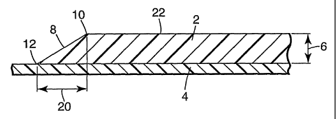
Referring now to the specific details of figure 1, it is a cross sectional
view of a
coated substrate, looking in the machine direction. The figure shows coating
material 2 of
a desired thickness 6 coated onto a substrate 4. Edge 8, with projected width
20, is the
tapered coating material edge, extending generally from point 10 to point 12.
Point 10
indicates the point where edge 8 meets the surface 22 of the bulk of coating
material 2,
having a desired thickness 6. Point 12 indicates the endpoint of coating
material edge 8,
where the thickness of coating material 2 goes to zero.
The slope of tapered edge 8 may be comparatively shallow. Figure 1 shows that
edge 8 has a width 20 (a dimension in the cross direction of the web), which
may vary
depending on the coating material, its thickness, and the techniques used to
apply the
coating material. For a coating material that is applied by conventional
methods, such as
by conventional die coating methods, to have a desired thickness 6 in the
range from about
10 microns to about 70 microns, width 20 may typically be in the range of a
few
millimeters, e.g., about 1, 2, or 3 millimeters. (As described below, it is an
advantage of
CA 02448012 2003-11-21
WO 02/101854 PCT/US02/08217
certain embodiments of the invention that the degree of taper of edge 8 can be
caused to be
relatively steeper by using preferred coating techniques described herein. In
those
instances, the width 20 of a coating material edge can be reduced.) The width
20 of the
edge of the coating material in figure 1 is not to scale relative to, e.g.,
the thickness 6 of
the coating material.
Referring now to figure 1 a, edge material 16 is coated to contact and at
least
partially cover tapered coating material edge 8. In the illustration, edge
material 16 is
ideally shown to substantially cover tapered edge 8. The combined thickness of
the
coating material edge 8 and edge material 16, across width 20, produces a
desired,
relatively uniform thickness profile 24 that uniformly approximates and
preferably equals
desired coating thickness 6. Also shown is the bulk of edge material 16 having
a desired
thickness 14, and including its own tapered edge.
This embodiment of the invention can be useful to improve the thickness
profile of
coating materials coated by conventional methods, by augmenting the thickness
of the
coating material edge. In some product constructions such as batteries it can
be desirable
that the thickness of the exposed amount of coated material be uniform.
Referring again
to figure l a as an example, the exposed surface of coating material 2 has a
uniform
thickness 6 provided by the bulk of the coating material across the substrate,
ending at
point 10. In battery product constructions, the coated substrate will be wound
or stacked
into layers wherein the area of the coating material edge, beginning at point
10 and
extending to the termination of edge material 16, will have the properties of
the edge
material 16. Edge material 16, when wound or stacked into a battery product
component,
can perform useful functions such as protecting the enclosed coating material
2, or acting
as an insulator between components of the battery. As such, edge material 16
can be made
up of material that accomplishes one or more of these functions, e.g., a
barrier material, a
non-active battery material, an insulating material, etc.
Still referring to figures 1 and 1a, the coating material and the edge
material can be
applied to a substrate using any techniques and equipment that can produce the
depicted
arrangement of materials on a substrate. Many types of such equipment will be
understood to be useful by a skilled artisan to continuously coat different
materials onto a
substrate with adjacent, contacting edges.
11
CA 02448012 2003-11-21
WO 02/101854 PCT/US02/08217
Preferred coating methods and equipment involve die coating methods (including
extrusion methods by die-coating) and equipment that allow edge material and
coating
material to be continuously coated onto different areas of a substrate with
their edges
being in contact. Examples of equipment include dies that allow for the
separate flow of
coating material and edge material from different coating apparatuses. Also
preferred can
be equipment that allows for the separate flow of coating material and edge
material from
different orifices of a single coating apparatus, e.g., through separate but
closely spaced
slots of a single coating die that has the capacity to coat multiple flows of
materials onto a
single substrate.
A variety of multi-orifice coating apparatuses are known, including those
described
in W095/29763, as well as multi-cavity coating apparatuses that include
multiple closely
spaced holes designed to approximate a continuous slot, and extrusion-coating
dies.
Specific examples include multi-slot dies having two or more continuous,
substantially
parallel slots, including those types referred to in the coating arts as dual
slot extrusion
dies, slot fed knife dies, and fluid bearing dies.
Examples of multi-orifice, multi-slot coating equipment are shown in figures
2a
and 2b. Referring specifically to figure 2a, it is a side view of a two-
cavity, two slot dual
extrusion die. Coating head 40 includes two channels, 42 and 44, defined by
three
separate members 46 which together define the channels 42 and 44, terminating
at the end
of the coating die or coating head, the end being sometimes referred to as the
lip, and
being placed in close proximity to the substrate during coating. Coating
material 2 and
edge material 16 flow through the channels for coating onto a substrate 4
while substrate 4
travels past coating head 40. Because figure 2a is a side view of the coating
process, the
figure illustrates coating material 2 first being coated onto substrate 4, and
edge material
16 being coated second (but nearly simultaneously) and adjacent to and in
contact with
coating material 2.
As will be appreciated by those skilled in the arts of coating methods and
coated
materials, the exemplary coater head 40 of figure 2a and its structure and
components can
take alternative forms, as desired, and according to known principles. For
instance,
members 46 are illustrated in figure 2a to terminate in cornered tips. One or
more of these
tips may instead be pointed or rounded. Different embodiments of these coater
heads are
known by a variety of names in the coating arts, such as, very generally,
"dual extrusion
12
CA 02448012 2003-11-21
WO 02/101854 PCT/US02/08217
dies," or more specifically as "slotted knife," or otherwise. Figure 2b, for
example, shows
a coater head 54 that includes pointed members 48 and rounded members 50, the
combination of which defines channels 42 and 44, for coating material and edge
material.
Rounded members 50 further define channel 52, which in this coater can be used
to pull
vacuum from substrate 4 prior to coating coating material 2 and edge material
16.
Figure 3 is a front view of a coater head 41. Looking at figure 3, it
illustrates how
coating material 2 and edge material 16 can be applied to different areas of a
substrate
moving past the coater head 41. In general, this is accomplished by using
coating
equipment having multiple manifolds for coating different materials, with the
different
manifolds coating different areas or "stripes" onto a moving substrate.
According to the
invention, the edges of the different stripes contact each other when applied
to a substrate.
As illustrated in figure 3, selectively coating different areas of a moving
substrate
can be accomplished by selectively preventing coating material from flowing
out of
selected portions of one orifice (here a slot) of a coater head, while
allowing flow of edge
material from the corresponding portion of the other slot, and vice versa.
Referencing
figure 3, shims are placed at portions 64 of slot 70, and at portion 66 of
slot 72. This will
prevent coating material 2 from being coated onto a substrate surface moving
past portions
64, but allow coating of the coating material at portion 60. Conversely, a
shim at portion
66 of slot 72 prevents coating of edge material where coating material has
been coated
from portion 60 of slot 70, and edge material flows from portions 62 of slot
72, to place
edge material on substrate surfaces where no coating material is coated
because of shims
64 in slot 70. The overall effect provides a complementary system of coating
edge
material 16 and coating material 2 onto different areas of a substrate 4
traveling past
coating head 40. As described above, the interface between an edge of the
coated coating
material 2 and the coated edge material 16 can have a desired, preferably
uniform,
thickness profile, preferably where the thickness of the material in bulk
coating 2, the
thickness of material at the coating material edge, and the thickness of the
bulk coating of
edge material, will be approximately the same when wet and/or dry, e.g.,
within 5 or 10
percent of each other.
As further description of embodiments of the invention, certain coating
techniques
can be used whereby edge material can be coated with coating material in a
fashion such
that the edge material acts as a boundary against which coating material is
coated,
13
CA 02448012 2003-11-21
WO 02/101854 PCT/US02/08217
optionally and preferably allowing the formation of an improved thickness
profile of the
edge of the coating material, e.g., with an improved edge shape having more
squareness,
less taper, and a narrower width.
The coating material can preferably be immiscible with the edge material at
coating conditions such that the coating material forms an edge of a desired
shape at the
interface between the edge material and the coating material. "Immiscible" can
refer to
materials that form two identifiable phases when they come into contact with
each other.
As specifically used herein, two materials, i.e., coating material and edge
material, coated
onto a substrate as films contacting each other at their respective edges are
considered to
be immiscible if there is an identifiable separation between the two.
Immiscibility of the
materials can be affected by a number of factors that relate not only to the
composition of
the different materials, but that also relate to the overall coating
environment and the
coating techniques used. Thus, "immiscibility" is not an absolute function of
the specific
materials that are being considered. Instead, immiscibility can be environment-
specific,
also relating to environmental factors such as temperature and other
conditions used in
causing the different materials to interact. For example, the compositions of
the materials
can be selected to inhibit their miscibility. Composition can include both the
chemical
makeup of ingredients of materials and the amounts of different ingredients
included in
different materials (e.g., as measured by solids percentages). Other features
of the
materials that can also affect miscibility include temperature or viscosity of
the different
materials and the methods used to coat the different materials onto a
substrate. Based on
these factors, different or like materials can be immiscible materials, and
environmental
factors can allow different or like materials to maintain a separation when
coated to
contact each other. Some coating techniques can be particularly useful in
coating
materials onto a substrate while maintaining a separation between the
materials. Such
techniques include those that promote laminar flow of the materials and
minimize
turbulent interaction at the edges of the materials that come into contact.
Differences in
chemical composition, viscosity, temperature, flow rates, shim thicknesses, or
slot overlap
of separate stripes of materials being coated can also be used to encourage
separation
between the materials when coated to contact each other. Also, the respective
coating
thicknesses of each of the coated materials can affect the miscibility or
otherwise influence
the shape of the, coating material edge. It can be preferred that the wet
coating thicknesses
14
CA 02448012 2003-11-21
WO 02/101854 PCT/US02/08217
of materials being coated are similar or approximately the same. For example,
it can be
preferred that the wet thicknesses of the edge material and the coating
material, where the
edge of the edge material contacts the edge of the coating material, are
essentially the
same, for example are within ten or five percent of each other.
Referring now to figure 4, coating material 2 is coated adjacent to and in
contact
with edge material 16. The materials are immiscible as coated, so they do not
substantially mix or combine, but preferably maintain substantial separation
at interface
28.
Figure 4 represents an idealized embodiment of square edges prepared according
to
the invention, where both materials exhibit approximately or perfectly square-
cornered
edges at interface 28, and the thickness profile across the bulk coating
material, at the
interface 28, and across bulk edge material 16, is uniformly equal to desired
thickness 6.
This is in contrast to figure 1, which shows a coating material 2 having an
edge 8 that
includes a relatively shallow taper.
The invention also contemplates coatings of all intermediate degrees of slope
or
taper, e.g., degrees of "squareness" of a coating material edge (possibly even
an edge
where the coating material edge slopes over the edge material edge, wherever
this
configuration might be useful). Different degrees of slope or different
degrees of
"squareness" or taper can be achieved by selecting coating techniques that
increase the
slope of a coating material edge, i.e., increase the steepness or squareness
of the edge.
These techniques are generally those techniques that work by causing edge
material to act
as a physical boundary against which the edge of the coating material forms. A
first
element of this embodiment can be the selection of materials or coating
conditions that
maintain a separation between the materials during and after coating, i.e., by
selecting
materials and coating conditions and coating techniques that cause the
materials to be
immiscible while coated. A second element can be the timing of the different
coatings.
Preferred results according to this embodiment can be achieved when the timing
of coating
the edge material relative to the timing of coating the coating material is
not sufficient for
an edge of either material to flow into the form of a taper. Preferred timing
can cause
edges of the different materials to contact each another either prior to,
during, or soon after
the moment or moments of their application to the substrate, so that the
interface of the
CA 02448012 2003-11-21
WO 02/101854 PCT/US02/08217
two materials at their edges cannot take the form of a taper, but instead, the
materials abut
each another at a fairly steep angle relative to the substrate.
Figure 5 illustrates an example of an intermediate degree of slope of a
coating
material edge. In figure 5, a coating material 2 is coated with and in contact
with an edge
material 16, e.g., from different orifices of a single coater head. The width
20 of the edge
of coating material 2 can be less than a width of a coating material coated
without an edge
material, e.g., the width 20 of coating material 2 in figure 5 may be in the
range of
millimeters to fractions of millimeters, for example less than 1 mm, or 0.5
mm, e.g., 0.2 or
0.1 mm. An example of this is figure 10 where a 1-2 mm width in absence of
edge
material is reduced to 0.1-0.2 mm width with the edge material. In figure 10
the edge
material is not visible in the SEM but the effect can be seen by the reduced
taper of the
coating material. As stated, particular methods can most closely approximate
an idealized
square edge, as shown in figure 4.
As discussed herein, timing of coating of an edge material and a coating
material
may with some techniques, ideally be simultaneous, which could technically
mean that the
two materials are coated from the same orifice, e.g., coater slot, or from
different slots
located exactly next to each other. The materials can be coated in a nearly
simultaneous
fashion if coated from two different orifices that are located very near each
other and they
are coated onto a substrate that is moving very quickly past the coater head.
In this case, it
is possible for the edge of the coating material to contact the edge of the
edge material
even before both materials contact the substrate. When preferred multi-slot
die coating
equipment is used, the slots can be as near as possible to each other, causing
the timing
difference to be minimal, and even causing the edge material to come into
contact with the
edge of the coating material at a point before either of the two materials
comes into
contact with the substrate. For example, some coater heads can place separate
but
substantially parallel slots at distances in the range from about less than 1
him (thickness
of center wedge) to about 5 mm. The same equipment can be used to coat a
substrate
traveling past the coater head at a speed in the range from about 3 to about
1000 feet per
minute. The result is the nearly simultaneous application of the different
materials from
the coater head, with exemplary timing differences being significantly less
than a second,
e.g., in the range from about 0.001 to about 1.0 seconds.
16
CA 02448012 2009-08-25
60557-7033
The invention will be appreciated by the skilled artisan to be useful with a
variety
of different coating materials, edge materials, substrates, and possibly other
components of
individual product constructions that include a coated substrate.
The substrate can be any material that may be useful for a desired product
construction, and upon which edge material and coating material can be coated.
Examples
of useful substrate materials include film or film-type materials that may
include paper,
polymeric materials such as polyethylene, polyester, polypropylene, silicone
release liners,
metallic foils and screens and other metals coated on paper or polymeric
materials, any of
which may be first coated with other useful materials, e.g., to affect a
surface
characteristic of the substrate such as surface tension, or such as with a
primer to promote
adhesive properties.
For some preferred battery constructions, useful substrates can include
aluminum
foil, copper foil and polymeric films such as polyester and others that will
be appreciated
by the skilled artisan. As known to those skilled in the art, the substrates
should not react
with the coated material.
The coating material and edge material can he any ina erials that can be
coated into
a preferably continuous and relatively uniform film on the surface of a
substrate.
Application areas include photographic, photothermographic, magnetic data
storage,
solvent adhesives, PSA adhesives, optical elements, fuel cells, as well as
batteries.
A particular example of a product construction that can benefit from (lie
coating
methods described herein are methods of producing certain electrochemical
cells, such as
batteries, for example batteries that include a stacked or rolled multilayer
construction, for
example, as is illustrated in United States Patent Number 5,360,654.
When a method of the invention is used to construct an electrochemical cell,
e.g., a
battery, the coating material can be an electrode material such as a cathode
material.
Cathode materials are known in the art of batteries, and can be prepared from
materials
that are generally known and useful for electrodes or other components of an
electrochemical cell. These can include an electrode active material, an
electrically
conductive material, an ionically conducting polymer, an electrolyte salt, and
optionally a
solvent.
17
CA 02448012 2003-11-21
WO 02/101854 PCT/US02/08217
The active material can be any of a variety of active materials known to be
useful
in electrodes, including oxide materials. The exact material used can be
chosen based on
various factors. As one example, the active material for use in lithium
polymer batteries
should be capable of storing lithium ion.
Examples of suitable active materials include LiCo02, LiNi02, Co-doped
Li,tNi02, Li,tMn204, LiXMn02, V205, V6013, Li,V308, Ba2SmNiO5, SmMnO3,
Sm3Fe5O12,
EuFeO3, EuFe5O12, EuMnO3, LaNiO3, La2CoO4 and LaMnO3 (including the charged
and
discharged forms of these materials. In primary batteries, the cathode can be
fluorinated
carbon, S02C12, Ag2V4011, Ag2CrO4, V205, AgCl, MoO3, FeS, CuS, sulfur,
polysulfide,
and an 02 or SO2 electrode. Particularly preferred electrode active materials
include
vanadium oxide and lithiated vanadium oxide. The amount of active material
used can be
any useful amount, as will be understood by one of ordinary skill.
Electrically conductive material can be included in the electrode to aid in
electric
conductivity of the electrode. Useful electrically-conductive materials are
well known,
and can include, for example, carbon, e.g., carbon black or graphite, lamp
black, coke,
carbon microbeads, carbon fibers, carbon flakes, copper powder, or other metal
powders.
The actual electrically-conductive material used in any particular electrode
can be chosen
based on various factors, such as the other materials of the electrode, or the
electrochemical system. Often, carbon black or graphite are preferred. Useful
amounts of
the electrically conductive material will be understood by the skilled
artisan, for any
particular electrode, and can be any amount that aids in electronic
conductivity of the
electrode. An example of a useful amount of electrically-conductive material
can be in the
range from about 1 to about 10 weight percent electrically-conductive
material, based on
the total weight of all electrode components, excluding solvent.
An ionically conductive polymer is included as an electrode component as a
binder
to hold the electrode components together in the form of a functioning mass
that is
ionically conductive. The polymer can be chosen to provide desired adhesion
and
conductivity properties. The ionically conductive polymer may be a single type
of
polymer, or may be a mixture of two or more ionically conductive polymers. Or,
the
electrode may include a mixture of one or more ionically conductive polymer
with another
polymer that is not ionically conductive.
18
CA 02448012 2009-08-25
60557-7033
Ionically conductive polymers for use in electrode materials are well known
and
commercially available. One exemplary class of ionically conductive polymers
is the
class of polymers that are derivatives of monomers comprising an oxygen-
containing
monomer or a nitrogen-containing monomer. Preferred ionically conductive
polymers are
capable of conducting ions at room temperature, and are capable of
dissociating alkali
metal salts.
Examples of suitable ionically conductive polymers include: polyethers of the
general formula
I IO(CH2CH2O),(CH7CI IRO),1-l,
where
x and y are mole fractions between 0 and 1, and x + y =1, and
R is:
a straight chain or branched alkyl group having the formula CnH2õ+, where
nisIto12;
a straight chain or branched arylalkyl group having the formula ArCj I2n'
where n' is I to 12 and Ar is an aromatic moiety (e.g. phenyl and naphthyl);
an ethylcnically unsaturated group having the li>rnnula CHR'=C(R')"7.C1 l 12i
,
where R' is H or methyl, Z, if present, is -0-, -S-, -SO-,
-SO2-, -NH-, -C(O)-, or -C(O)O-, and n" is 0 to 12; or,
an oligoether of the general formula R.'(CIIR'CH,O),,, where R' and n are
as defined above.
Other examples of useful ionically conductive polymers include polysiloxanes,
polyphosphazenes, and polyacrylates.
One class of preferred ionically conductive polymers include polyalkylenoxide
homopolymers or copolymers derived from monomers such as ethylene oxide,
propylene
oxide, butylene oxide, and allyl glycidyl ether. Such polymers are
commercially available
TM
under such designations as DAP from Dai-Ichi-Cogyo Seiyaku, Japan and
TM
polyethyleneoxide available from Union Carbide under the designation Polyox.
Examples
of such ionically conductive polymers and their preparation are also
described, for
example, in United States Patent Number 4,303,708.
19
CA 02448012 2009-08-25
60557=7033
Useful amounts of ionically conductive polymer used in an electrode can be any
amount that will act to bind the other ingredients into a useful electrode, as
well as provide
desired conductivity. Exemplary amounts may be, for example, in the range from
about
to about 40 weight percent conically conductive polymer, based on the total
amount of
5 all electrode components, more preferably from about 26 to about 32 weight
percent.
Other polymers that are not ionicalty conductive may also be used in the
electrode.
Such polymer may be included to improve mechanical integrity or as a low cost
binder.
Examples include polyvinylidenefluoride (PVDF), polyacrylonitrile (PAN) and
polyvinylpyrrolidinone (PVP), ethylene-propylene-diene (EPDM) terpolymer and
10 emulsified styrene-butadiene rubber, among others. If non-ionically-
conductive polymer
is included in an electrode, it can be used in any amount that is useful,
e.g., to provide a
desired property, such as mechanical integrity, and is preferably included in
an amount in
the range from about 0 to about 50 percent by weight of the total weight of
polymer (the
total amount of conically-conductive and non-conically-conductive polymer).
The electrolyte salt is a highly dissociated salt capable of being dissolved
in the
conically conductive polymer. For lithium polymer batteries, the salt is
typically a lithium
salt.
haectrolyle salts are well known in the arts relating to electrochemistry and
electrochemical systems. Specific examples of preferred lithium salts are also
well known
and include lithium hexafluoroarsenate, lithium perchlorate, lithium
hexafluorophosphate,
lithium trilluoroborate, lithium trifluoromethanesulfonate, lithium
bis(trilluoromethanesulfonyl)imide, lithium bis(perfluoroethanesulfonyl)imide,
lithium
tris(trifluoromethanesulfonyl)methide. See also United States Patent Serial
Numbers 6,280,883 and 6,294,289. Particularly preferred are lithium
hexafluorophosphate and lithium bis(trifluoromethanesulfonyl)imide.
The amount of electrolyte salt included in the electrode components should be
enough to provide for a functioning electrode, e.g., to result in a sufficient
level of ionic
conductivity. Those of ordinary skill will appreciate amounts of the salt that
will be useful
in electrodes prepared by methods described herein. A useful amount for a
particular
electrode can depend on a variety of factors such as the particular salt
chosen and the types
CA 02448012 2003-11-21
WO 02/101854 PCT/US02/08217
and amounts of the other electrode components. While other amounts may be
found to be
useful, examples of useful amounts of electrolyte salt can be in the range
from about 3 to
about 15 weight percent based on the total weight of all electrode components,
preferably
from about 5 to about 10 weight percent.
Other optional ingredients may also be included in the electrode components,
as
will be understood by those of ordinary skill. These optional ingredients may
include
materials such as pore formers, surfactants, flow agents, antioxidants, and
solvents.
Exemplary solvents may include ethylene carbonate, propylene carbonate,
dimethyl
carbonate, dietheyl carbonate, dimethyl adipate, tetramethylene sulfone, gamma-
butyrolactone, dimethylformamide, dioctyl phthalate, tetrahydrofuran,
polyethylene glycol
dimethyl ether, polyethylene glycol, or combinations of these and other
solvents.
The edge material can be any material that can be coated as described herein.
The
particular material used in a specific edge material can be selected to
provide desired
properties for a particular product construction. Moreover, properties of the
edge material
can be selected to interact well with the substrate and the coating material,
for example to
be coatable on the substrate and to be either coatable onto the coating
material or
immiscible with the coating material, to result in a desired thickness profile
at the coating
material edge, or to result in a desired shape of the coating material edge.
In some product constructions, such as an electrochemical cell, the edge
material
can be a non-active battery component, such as an insulating material, and can
also or
alternatively be chosen to act as a barrier to protect the coating material
when the layers of
the coated substrate are stacked or wound. Useful barrier materials may act as
a barrier to
air, to light, to water (any type of water including moisture in the air or
aqueous water), or
as a barrier to any other material or debris generally, as needed for
particular product
constructions. Additionally or alternatively, a preferred edge material can be
electrically
insulating, such as in the case of edge materials for batteries.
Some examples of edge materials can be coated in a solvent form, and later
heated
to remove the solvent. Alternatively, an edge material may be a coatable
(e.g., film
forming and extrudable) composition that could be chemically cured,
thermoplastic, or
thermoset, if desired.
As mentioned, the edge material, meaning the final form of the edge material
after
drying or curing, may perform some useful function in a product construction.
For certain
21
CA 02448012 2009-08-25
60557-7033
product constructions, therefore, some types of edge materials will not be
appropriate. For
example, certain product constructions would prefer a barrier material that
takes the final
form of a solid that is cohesive and not tacky or sticky, as would be a
material that could
be considered a pressure sensitive adhesive (PSA) or an elastomeric liquid.
Thus, some
embodiments of the invention include a barrier material that is neither a PSA
nor an
elastomeric liquid in its final form (e.g., after processing from a solution
or otherwise).
Exemplary polymeric inactive materials may comprise an electrically insulating
polymer such as polyurethane, polycarbonate, polyolefin, polyvinylether or a
polyacrylate
or poly(ineth)acrylate, etc. Likewise, monomers such as isocyanate/(polyol or
polyamine)
or acrylates or oligomers may be coated and then heat or UV cured.
A substrate that has been coated as described with a coating material, an edge
material, or both, can be processed in any desired fashion, to produce any
desired product
configuration. Examples of useful subsequent or intermediate processing steps
might
include additional coating steps; heating or cooling steps for affecting the
coatings with
temperature, e.g., for drying, solidifying, or curing, laminating, slitting,
UV or electron
beam curing, calendaring or any other processes that can be used to process
coated films.
In electrochemical cell product configurations, processing of the coated
substrate
may include steps of introducing other components of the battery and then
processing the
combination into a battery cell. The additional components may generally
include a
separator layer, negative electrode, and negative electrode current collector.
Those of skill
in the battery arts will understand how such components can be incorporated
with a
substrate coated as described herein to produce an electrochemical cell. See,
for example,
United States Patent Number 5,360,684 to Hydro-Quebec. e.g., at example 1, for
description of a cell assembly process. In broad terms, a coated cathode or
current
collector may be laminated to an electrolyte film, followed by a lithium foil
lamination
and finally a polypropylene film. For a description of equipment useful for
efficiently
producing a stack of battery components according to the invention, see also
United
States Patent Serial Number 6,547,229.
The coated substrate can then be stacked or rolled to produce a layered stack
of
substrates coated with coating material (e.g., cathode material), edge
material, and other
CA 02448012 2003-11-21
WO 02/101854 PCT/US02/08217
optional layers useful in batteries. Most preferably, a coated substrate can
be rolled into a
wound roll, preferably using a large radius core. The wound roll can then be
cut into
pieces that can be laid into a relatively flat-layered component of convenient
size for
battery applications and further processed into a battery.
Figure 6 shows an example of such a layered battery component. Referring to
the
figure 6a, which is a side view in one direction of a stacked battery
component, the figure
shows stacked battery component 102, that is made up of an anode layer 104,
separator
layers 106, a cathode current collector 108, and coated edge strips 110, which
in this view
conceal cathodes (see below). These layers can be prepared according to known
methods
and materials, and as described herein. For instance, anode layer 104 can
include any type
of materials useful in anodes such as lithium foil, lithium metal on a metal
or plastic
support, or other materials. Separator layers 106 may include a solid polymer
electrolyte,
a porous membrane, or other separator materials. Cathode current collector 108
may be
prepared of materials known in the battery arts, such as aluminum, stainless
steel or nickel
and coated edge strips 110 can be an edge material as described supra.
Figure 6b shows stacked battery component 102 in a top view. From this view
are
visible only anode layer 104, a portion of an edge strip 110, current
collector 108, which is
visible at the other edge of the stacked battery component 102 (at the bottom
of figure 6b),
and the exterior separator 106.
A view of the same stacked battery component 102 from a different side is
shown
in figure 6c. Starting from the right surface in the figure, figure 6c
illustrates the
structures of anode 104 being on an exterior surface, separated by a separator
layer 106
from cathode 112. A first edge strip 110 contacts a coated edge of the cathode
112, and
maintains a separation between separator 106 and anode 104, and one surface of
current
collector 108. The other surface of current collector 108 contacts a second
cathode 112,
also having an edge strip 110 coated at an edge of the cathode 112. The second
edge strip
110 maintains a separation between the current collector 108 and a second
separator 106.
Referring still to side view 6c, multiple stacks can be placed adjacent to
each other, by
placing the exposed surface 114 of anode 104 in contact with an exposed
surface 116 of an
identical stacked battery component, in a wound or stacked configuration.
Figure 6 illustrates how the edge of cathode 112 is covered by edge material
110,
providing an insulating barrier between the cathode 110, anode 104, and
current collector
23
CA 02448012 2003-11-21
WO 02/101854 PCT/US02/08217
108. Also apparent from figure 6 is the feature that the edge material can act
as a barrier
to protect and enclose the cathode 112 when the cathode is placed in a stacked
configuration with other components of a battery. The edge material 110 may
act as a
barrier to light, moisture, water, or other materials.
The stacked battery component 102 of figure 6 can be contrasted to a stacked
battery component that does not use coated edge material as described herein.
Figure 9
illustrates such a battery component, 120, having anode 124 and insulating
strip 130 at one
end of anode 124, both in contact with a separator 126. The insulating strip
prevents
contact between the anode 124 and the current collector 128. A first cathode
122 is
adjacent to the separator 126, which is adjacent to a current collector 128,
which is in turn
adjacent to a second cathode 122, next to a second separator 126. A second
insulating
strip 130 is on the other side of the second separator 126. The stacked
battery component
120 can be placed adjacent to identical stacked battery components, by placing
the
exposed surface 134 of anode 124 in contact with an exposed surface 136 of
second
separator 126, of an identical stacked battery component, e.g., in a wound or
stacked
configuration. When so wound or stacked, the second insulating strip 130 acts
to separate
and insulate current collector 128 from anode 124.
In preferred processing methods of making battery cathodes or other materials,
coating material and edge material can be stripe coated onto a substrate with
improved
manufacturing efficiencies. In general, alternating stripes of an edge
material and coating
material can be coated adjacent to each other, optionally with uncoated areas
separating
stripes of edge material.
One embodiment of a stripe-coated substrate is shown in figure 7. Figure 7
shows
substrate 4 and stripes of coating material 2 with edge material 16 coated at
each edge of
the coating material 2. The stripes of edge material are separated by uncoated
stripes of
exposed substrate 4, as indicated. Stripe-coating the substrate as illustrated
can allow
efficient production of multiple battery components from a single web. The
stripe-coated
substrate can be further processed as desired, for example to coat additional
layers onto the
stripe-coated materials, and by slitting, e.g., at the uncoated substrate
between stripes.
Another embodiment of a stripe-coated substrate is shown in figure 8, which
illustrates a similar stripe coated substrate, but without spaces between'
stripes of coated
edge material. In figure 8, a substrate is coated with alternating stripes of
cathode material
24
CA 02448012 2003-11-21
WO 02/101854 PCT/US02/08217
2 and edge material 16. This embodiment has advantages that are similar to the
those
described with respect to the coated substrate of figure 7, but differs in
that slitting will be
along a stripe of the coated edge material 16.
Example 1
A die (as described in W095/29763 and additionally illustrated in figure 2b)
with 2
cavities was used to coat edge barrier strips on either side of a primary
coating in a
continuous manner. Coatings were placed onto a 1.4 mm polyester backing.
Shims for each slot of a dual slot coater (as designated in figure 2b) were
prepared
so that openings allowed an edge of a non-active edge material to align with
an edge of a
cathode material (in this case active) coating to be delivered separately to
the web via each
of the two slots. The two coatings were coated in different orders in
producing different
samples, sometimes the cathode material being coated first and sometimes the
edge
material being coated first.
For the edge material, 21% (w/w) polyethyleoxide (Polyox WSR-N-80 MW
200.000, Union Carbide) was mixed with a solvent blend of 80 % acetonitrile
and 20%
toluene (w/w).
For the coating (in this case cathode) material, the following composition,
30%
w/w in 80:20 acetonitrile/toluene, was fed through the a slot in the die (slot
spacing as
defined by shim thicknesses was 0.007-0.020 inches (sharp center die wedge)):
62% w/w
LiV3O8 (3M), 29% w/w ethylene oxide/propylene oxide/allyl glycidyl ether
copolymer
("DAP", Dai-Ichi-Cogyo Seiyaku, Japan), 3% w/w/ Ketchenblack EC600JD carbon
black
(Akzo Nobel, Chicago, Ill.), 6% w/w lithium bis(trifluormethanesulfonyl)imide
salt (3M).
Samples of 43 different coating conditions were generated. The conditions
included:
coating vacuum .................. 0-1 inches of H2O
over bite ................................ 0-0.003 inches
coating gap ........................... 0.010-0.020 inches
1st slot pump ......................... 10-70.5 rpm
2nd slot pump ........................ 0-70.5, rpm
shim offset ............................ 0-0.0625 inches
web speed ............................. 25 fpm
CA 02448012 2003-11-21
WO 02/101854 PCT/US02/08217
web caliper ............................. 0.002 inches
coat width .............................. 3.5 inches
strip width .............................. 2 @ 0.25 inches
vacuum gap ............................ 0.006 inches
slot heights ............................. 0.02 inches.
SEMs were taken of several samples with both planar and cross-sectional views.
Figure 10 illustrates a cross sectional view showing an improved edge.
Although the edge
material is not visible in the SEM (magnification 400x) the inventive effect
can be seen by
the reduced edge width (0.1-0.2 mm vs.1-2 mm without the edge material). The
edge
tapers from a bulk thickness at the point designated "cathode" down to a
thickness of zero
at the point designated "dam." The large flake near the midpoint of the
coating material
edge is debris.
Example 2
Alternating stripes of Indicator Composition B ("indicator stripe") at 38%
solids
and Barrier PSA Composition ("PSA stripe") at 39% solids were coated onto an
untreated,
low-haze, 1.4-mil polyester PET transparent film backing using an extrusion
die. The
basic die is as described in W095/29763 with two separate manifolds and slots
for
supplying the Composition B (Bottom Manifold) and the Barrier PSA (Top
Manifold). A
precision gear pump was used to supply the PSA composition to the top manifold
and
another precision gear pump was used to supply the indicator composition to
the bottom
manifold. Each pump could be adjusted independently to control flow rate of
the
compositions to the die. The pump flow rates were set for 2.6 mil wet for the
indicator
stripe, and 2.9 mil wet for the Barrier PSA Edge. An arrangement of shims
allowed
distribution and delivery of the Barrier PSA Edge material (1 inch width)
adjacent to the
Indicator Composition B material (0.5 inch width). Different width, spacing,
and
registration of the edge stripes and center could be achieved by machining new
slot shims
for each manifold section. The die was mounted in an assembly on a precision
die mount
that allowed for adjustment of the engagement of the die with the web on the
back-up roll.
26
CA 02448012 2003-11-21
WO 02/101854 PCT/US02/08217
The striped coating was dried using a forced air oven located directly after
the die
station to provide a dry coating thickness of about 25 microns. Samples were
coated with
minimal transition disturbance zone between the adjacent barrier edge and
indicator stripe.
Example 3
Thin film coatings can be prepared by essentially solventless extrusion of
mixtures
of solid ingredients. The ingredients are intimately mixed by a variety of
methods and
melted and compressed through a flat orifice to produce a thin coating on a
substrate.
A cathode containing an active material such as V205, electrically
conductivity
material such as carbon black, an electrolyte salt such as lithium
trifluoromethanesulfate,
and an ionically conductive polymer binder such as polyethylene oxide would be
mixed in
proportions similar to example #1 but with no solvent or liquid add. The
mixture would
be fed to a single screw extruder with a temperature sufficient to melt the
polymer binder.
The mixture would be pumped under pressure by the internal action of the
extruder to a
flat exit orifice. The melted mixture would be,formed and cooled on a web
moving past
the orifice.
A second mixture would be prepared from a polymer or monomer binder. The
binder may contain additional ingredients to aid hardening of the binder when
subjected to
light, irradiation or heat, to aid in flow characteristics and other
modifications for final
characteristics. This second mixture would be extruded or pumped under
pressure with
the flow stream split into two parts. Each of the parts is pumped through an
orifice that
modifies the shape of flow and places the flow next to the edge of the coated
cathode thin
film.
The placement of the edge flow can occur just prior to the cathode film
forming,
oriented to be simultaneous or nearly simultaneous with the cathode film
forming, or just
after the cathode film forming. The transition interface between the edge
coating and
cathode film is a function of the material characteristics, orifice geometry,
and placement
of each of the orifices.
27