Note: Descriptions are shown in the official language in which they were submitted.
CA 02448539 2003-11-25
l .r
2002P03232WO
Description
Arrangement for supplying electrical power to a load by
means of a transmission path which has been split into
two parts
The invention relates to an arrangement for providing
an isolated supply of electrical power for an
electrical load.
In general, an electrical load is supplied with
electrical power in the form of a supply voltage or a
supply current via a single electrical cable from a
voltage source or current source.
Sometimes, an isolated (= DC isolated) power supply is
required for the load, without any conductive
connection between the load and the supply source. If
the electrical load is arranged at an electrical
potential which differs to a very major extent from
that of the power source, or very stringent
requirements with regard to electromagnetic
compatibility (EMC) have to be satisfied, supply via a
single electrical supply line is at least difficult.
Examples of applications such as these are current
measurement and voltage measurement in public power
supply facilities, and ECG, breathing or pulse
measurement on a patient during a magnetic resonance
imaging investigation carried out in parallel.
An arrangement is known in which light from a light
source, for example from a laser diode or a light-
emitting diode (LED), is transmitted to a photoelectric
transducer, where it is converted into electrical
energy, which is used to supply the load. In order to
transmit light, the light source and the photoelectric
transducer are optically connected to one another via
an optical waveguide or else via a free-beam
~ CA 02448539 2003-11-25
2002P03232WO
- la -
arrangement. An isolated, optically operated supply
system such as this for an electrical
CA 02448539 2003-11-25
2002P03232WO
- 2 -
sensor is described, for example, in "Sensors and
Actuators A", Volumes 25 to 27 (1991), pages 475 to
480. The light from a laser diode is transmitted via an
optical waveguide to a photoelement array, which
converts it to the electrical energy for the sensor.
The measurement data from the sensor is likewise
transmitted optically via an optical waveguide.
However, owing to the special components that are used,
in particular the high-power laser, the photoelement
array and the optical plug connections, this supply
system is associated with not inconsiderable
complexity.
An arrangement is also known, in which the electrical
energy is obtained from the immediate area surrounding
an electrical sensor that is to be supplied, for
example inductively from a high-voltage network or
photovoltaically from solar radiation. However, this
arrangement for supplying power is subject to the
undesirable side effect that no electrical power is
available when the high-voltage network is not
operating, or when the sun is not shining. An
arrangement which draws its electrical power from the
high-voltage network is described in DE 25 46 694 Al.
Another arrangement for providing an isolated supply of
electrical power for an electrical load is disclosed in
DE 44 42 677 Al. In this case, a radio transmitter
transmits energy in the form of radio waves to a radio
receiver, which converts the radio waves to the
electrical power for the electrical load. If the load
is a sensor, then the measurement data from the sensor
is also transmitted by radio. This arrangement thus
allows DC-isolated power and data transmission without
any cables. Legal regulations relating to radio traffic
restricts the capability to use this arrangement,
however.
CA 02448539 2003-11-25
2002P03232W0
- 3 -
A further known approach for an isolated power supply
for a load which is, in particular, at a high-voltage
potential is to supply radio-frequency electrical
energy to a capacitor which is resistant to high
voltages, or to a capacitive divider which may be
present in any case for voltage measurement. The
capacitor or the capacitive divider in this case
bridges the potential difference. One disadvantage is
that undefined impedance ratios may occur. This is
because, while the capacitor or the capacitive divider
is used as the forward line for the radio-frequency
power, the return line is provided in a largely
undefined manner via a conductor to ground capacitance
of an existing high-voltage overhead line and/or via an
adjacent item of equipment. In order nevertheless to
ensure operability, a relatively high supply frequency,
for example of > 10 MHz, is required. However, the
arrangement then overall acts as a transmitting
antenna, which on the one hand leads to an undesirable
loss of energy due to radiated emissions, and on the
other hand leads to conflicts with the already
mentioned legal regulations relating to radio traffic.
A radio-frequency signal is also transmitted by means
of capacitive components in the arrangement disclosed
in DE 910 925 for controlling the drive for gas and
steam discharge paths. A first capacitive branch
element is provided for the forward direction, and a
second capacitive branch element for the backward
direction. The radio-frequency signal is, however, not
used for supplying power but, in fact, for controlling
an initiation circuit which is associated with the
high-voltage potential.
DE 29 11 476 Al describes a further development of the
transmission path disclosed in DE 910 925 for an
arrangement for supplying power to a load that is at a
high-voltage potential. The transmission path is in
CA 02448539 2003-11-25
2002P03232W0
- 3a -
this case in the form of a symmetrical filter chain
formed by means of series capacitors and parallel
inductors. The
CA 02448539 2006-02-24
20365-4789
4
parallel inductors were expressly also included in the
arrangement in order to reduce the load on the radio-
frequency generator from the provision of the wattless
component, and in order to compensate for isolation
differences occurring between adjacent capacitors. However,
owing to the large number of individual components required,
the arrangement is complex to implement.
The invention is now based on the object of specifying an
arrangement for supplying electrical power to an electrical
load, which ensures that the power is supplied in as simple
a manner as possible and, at the same time, does not lead to
any conflicts with the legal regulations for radio traffic.
This object is achieved by an arrangement for an isolated
electrical power supply for an electrical load as described
hereunder.
The arrangement according to the invention comprises at
least:
- a generator for producing a supply signal,
- a transmission path which contains two separate
branch elements, with
- the first branch element being designed for
transmission of the supply signal in the direction from the
generator to the load, and the second branch element being
designed for transmission of the supply signal in the
direction from the load to the generator,
- two branch elements are each connected to the
generator and to the load such that a closed circuit is
formed for the supply signal,
CA 02448539 2006-02-24
20365-4789
4a
- the two branch elements have means for isolation
and
- the load can be supplied by means of the supply
signal with an electrical power of at most 100 mW.
The invention is in this case based on the
knowledge that defined impedance ratios in the forward
direction and in the backward direction of the supply signal
can be achieved
CA 02448539 2003-11-25
2002P03232WO
- 5 -
on the basis of a transmission path which is provided
by means of two separate branch elements. The supply
circuit is then no longer closed via an undefined air
gap, but via a branch element which is intended for use
as the return line for the supply signal. The two
branch elements are, in particular, formed such that
they are completely isolated from one another, that is
to say there is no electrically conductive connection
between the two branch elements except at the location
of the generator and of the load.
Owing to the defined impedance ratios as well as the
low load power, the supply signal may in particular be
at a relatively low supply frequency, for example of
- 1 MHz. The supply signal is transmitted in both
branch elements by cables and, in particular,
electrically. This largely suppresses radiated radio
emissions from the supply signal, so that the legal
regulations are not infringed by the radio traffic.
Owing to the low transmission losses - in particular,
there is no undesirable radiated emission of supply
power on the transmission path - and owing to the low
load power, it is possible to use a supply signal
generator which is designed for a relatively low power
level and thus costs little.
Specifically, it has been found that the parallel
inductors which are used in the arrangement that is
known from DE 29 11 476 Al can be omitted without any
significant adverse effects on operation. This is true
even if the load is supplied via the supply signal with
only a low power level, for example of at most 100 mW.
The supply signal generator can itself apply the
charging power level which may be required for the
branch elements in this power range. Special
precautions for this purpose are equally unnecessary as
CA 02448539 2003-11-25
2002P03232WO
- 5a -
a special design of the generator. Overall, the
omission of the parallel inductors and the low-power
CA 02448539 2006-02-24
20365-4789
6
configuration of the generator result in a very simple and
low-cost arrangement for an isolated power supply for a
load.
The arrangement can be used particularly advantageously when
there is a potential difference between the location of the
load and that of the generator. In this case, the isolated
power supply is particularly advantageous. In particular,
the generator may be at ground potential and the load at a
high potential, for example at a potential of several tens
of kilovolts.
Furthermore, the two branch elements are preferably arranged
closely adjacent to one another. This reduces the space
required for the arrangement. In addition, close physical
proximity between the two branch elements prevents
intrinsically undesirable radiated emission of supply
energy. The two branch elements which are respectively
intended for the forward direction and the backward
direction have a similar effect to a bifilar conductor
arrangement, in which mutual compensation is provided for
the radiated emission response. In particular, the two
branch elements are accommodated alongside one another in an
isolator, thus reducing the costs for voltage isolation
between the two branch elements. It is at least possible to
use a common isolator housing.
The transmission path of the arrangement can preferably be
used not only for supplying power but also for some other
purpose, for example for voltage measurement. In this case,
the arrangement for supplying power can be integrated in
some other equipment which is provided in any case, thus
making it possible to further restrict
CA 02448539 2003-11-25
2002P03232WO
- 6a -
the costs for the arrangement. In particular, the
transmission path may also be used for detection
CA 02448539 2003-11-25
2002P03232W0
- 7 -
of the electrical voltage between the location of the
load and ground.
In another refinement, the branch elements each contain
at least one reactance as a means for isolation. In
this case, it is particularly advantageous to use a
capacitance, which can be used well for the desired
isolation. In particular, each of the branch elements
may also include a standardized or series-production
component, for example in the form of a wound capacitor
bank. This results in a particularly low-cost
implementation. However, an inductance may also be used
as the reactance.
It is advantageous for the supply signal to be at a
supply frequency which is between about 1 kHz and about
1 MHz. Radiated emissions of supply energy can be
suppressed well in this frequency range. Furthermore,
the lower limit mentioned is far enough away from a
mains system frequency that is used for public power
supply facilities (DC, 50 Hz or 60 Hz), and is
sufficiently far away from the harmonics of this mains
system frequency which may be relevant for measurement
and evaluation purposes, so that any influence can be
precluded.
An arrangement also exists which is operated with a
supply signal in the form of a DC signal. This prevents
radiated emissions in any case. Any potential
difference in this arrangement is preferably bridged by
means of inductances provided in the branch elements.
The load which is supplied with electrical power may,
for example, be a test set, in particular an ammeter.
The transmission path may then be used not only for
transmission of the supply signal but also, in
particular, for electrical transmission of a
measurement signal which is determined by the test set.
CA 02448539 2003-11-25
2002P03232WO
- 7a -
A measurement signal frequency which is intended for
this purpose is preferably not the same as the supply
frequency, in order to avoid any influence. In
principle, however,
CA 02448539 2003-11-25
2002P03232WO
- 8 -
the same frequency range may be used for the
measurement signal frequency as for the supply
frequency. A cost saving can be achieved by integration
of different functions in the transmission path.
In principle, it is also possible to transmit the
measurement information determined by a load in the
form of a test set via an additional transmission path.
The transmission paths which are used for supply signal
transmission and for measurement signal transmission
are then designed to be isolated from one another. They
may also use different transmission principles, for
example electrical and/or optical transmission. This
results in particularly good isolation between the
supply signal and measurement signal.
Preferred exemplary embodiments of the invention,
although these are in no way restrictive, will now be
explained in more detail with reference to the drawing.
For illustrative purposes, the drawing is not to scale,
and certain features are illustrated schematically. In
detail:
Figure 1 shows an arrangement, which is integrated in
a capacitive voltage converter, for an
isolated power supply,
Figure 2 shows an arrangement for an isolated power
supply for a test set, using optical
measurement signal transmission,
Figure 3 shows an arrangement for isolated power
supply for a test set, using electrical
measurement signal transmission, and
Figure 4 shows a further arrangement for an isolated
power supply for a test set, using optical
measurement signal transmission.
Mutually corresponding paths are provided with the same
reference symbols in Figures 1 to 4.
CA 02448539 2003-11-25
+ = 2002P03232W0
- 9 -
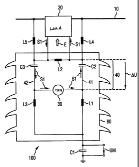
Figure 1 shows an arrangement 100 for an isolated power
supply for a load 20. The load 20 is arranged adjacent
to a high-voltage conductor 10, and is thus at the
high-voltage potential, that is to say at a potential
of at least several tens of kilovolts.
Power E is supplied to the load 20 via a supply signal
S1, which is transmitted by means of a transmission
path 40. In order to ensure isolation, the transmission
path 40 in the example shown in Figure 1 contains two
transmission capacitances C2 and C3, across each of
which a potential difference DU is dropped, which forms
the majority of the conductor-ground voltage of the
high-voltage conductor 10.
The supply signal Si is produced, for example at a
frequency of 100 kHz, by a generator 30 which is
effectively at ground potential. The supply signal S1
is fed into a first branch element 41, which includes
the transmission capacitances C2, of the transmission
path 40, and is transmitted to the load 20. The power E
is drawn in a manner which is not illustrated but which
is known per se from the supply signal Sl in the load
20, and is made available to the load 20 for operation
of, in particular, electronic components there. In this
case, the power E which is drawn from the supply signal
Sl may normally be temporarily stored initially in an
electrical energy store, for example in the form of a
capacitor.
In contrast to a first known arrangement, in which the
backward direction between the load 20 and the
generator 30 is formed via an air gap whose impedance
value is relatively undefined, the transmission path 40
in the arrangement 100 has a second branch element 42.
The latter contains the second transmission capacitance
C3, which preferably has the same capacitance value as
the first transmission capacitance C2. After passing
CA 02448539 2003-11-25
2002P03232W0
- 9a -
through the load 20, the supply signal Si is fed back
in the second branch element 42 to the
CA 02448539 2003-11-25
2002P03232WO
- 10 -
generator. The second transmitter capacitance C3 thus
also ensures a well-defined impedance value for the
transmission in the backward direction. A closed
circuit is then formed, with defined impedance
relationships. It is thus possible to operate at a
comparatively low supply frequency in the range between
1 kHz and 1 MHz, and also with a low supply power
level. This reduces the complexity required for
implementation of the arrangement 100.
In contrast to a further known arrangement, which
contains a transmission path in the form of a filter
chain, the two branch elements 41 and 42 of the
transmission path 40 in the arrangement 100 are
completely isolated from one another. This means that
no electrically conductive connection exists between
the two branch elements 41 and 42, except at the
generator 30 and at the load 20. They are electrically
isolated from one another in this area. In particular,
and in contrast to the known filter chain, no parallel
inductors are provided as connecting elements. It has
been found that this considerably simpler design can be
used by preference when the supply signal Sl is at a
relatively low supply power level. The generator 30 can
itself in this case provide the charging power for the
transmission capacitances C2 and C3. Overall, the load
20 can be supplied by means of the arrangement 100 in a
particularly simple and low-cost manner with a power
level of up to 100 mW. This is sufficient for operation
of many of the electronic circuits that are used
nowadays.
In order to avoid supply energy from flowing away
undesirably, two or more blocking inductances L1 to L5
are provided and each have inductance values such that
they have a very high impedance at the supply frequency
and, in the ideal situation, represents an open
circuit. The blocking inductances L1 and L3 prevent the
CA 02448539 2003-11-25
2002P03232WO
- l0a -
supply signal S1 from flowing away to ground while, in
contrast, the blocking inductances L4 and L5 prevent it
flowing away via the high-voltage
CA 02448539 2003-11-25
2002P03232WO
- 11 -
conductor 10. The blocking inductance L2 forces the
supply signal Sl to flow to the load 20. For
illustrative purposes, the signal path for the supply
signal Si is indicated by arrows with a solid line in
Figure 1.
If necessary, the blocking inductances Li to L5 may
also have surge arrestors and/or damping resistors
added to them.
The blocking inductances L1 to L5 do not represent an
open circuit, but virtually a short circuit, at the
mains system frequency (= DC, 50 Hz or 60 Hz) for the
high-voltage conductor 10. At the least, they assume a
very low impedance value at this frequency. The two
branch elements 41 and 42 are thus connected in
parallel for the mains system frequency, and are not
connected in series, as at the supply frequency. The
transmission capacitances C2 and C3 which are connected in
parallel at the mains system frequency may therefore also
be used as a high-voltage capacitance for a capacitive
voltage converter. A voltage measurement signal UM for the
conductor-ground voltage of the high-voltage conductor 10
can then be tapped off from an additionally provided low-
voltage capacitance Cl. The arrangement 100 carries out
two functions. It is used for supplying power to the load
20 and for voltage measurement. One particularly simple
and thus advantageous implementation of the arrangement
100 is obtained by integration in a commercially available
capacitive voltage converter. It is also advantageous with
regard to costs for the transmission capacitances C2 and
C3 to be standardized or series-production components, for
example in the form of a wound capacitor bank.
Depending on the physical form of the transmission
capacitances C2 and C3, they may also have a series
inductance. This is the case, for example, with the
CA 02448539 2003-11-25
2002P03232W0
- lla -
wound capacitor bank that has been mentioned. It is
then advantageous for the supply frequency (which in
principle can be chosen freely in the rate between
1 kHz and 1 MHz) to in fact correspond
CA 02448539 2003-11-25
2002P03232WO
- 12 -
to the series resonant frequency, which is formed by
the series inductance and the capacitance value of the
transmission capacitances C2 or C3. The two branch
elements 41 and 42 then represent a particularly low
impedance for the supply signal Sl.
The voltage difference between the two branch elements
41 and 42 is only very small (for example several tens
of volts), so that they can be isolated from one
another without any problems. In particular, they can
thus be located very closely adjacent to one another
and, for example, can also be accommodated in a common
isolator 80. This is a very cost-saving solution. The
close physical arrangement of the branch elements 41
and 42 also results in the radiated emissions of supply
power, which have already been greatly reduced in any
case by the low supply frequency, being virtually
completely suppressed.
Figure 2 shows another arrangement 200, which is
likewise intended for an isolated power supply for a
load 20. In the example in Figure 2, the load 20 is in
the form of a test set for detection of a current I
flowing in the high-voltage conductor 10. The test set
20 contains a measurement shunt 21 and measurement head
electronics 22, in which a measurement signal S2 for
the current I is determined. The measurement signal S2
is transmitted optically to a receiving and evaluating
unit 70, which is at ground potential. An optical
transmission path 50, for example in the form of an
optical waveguide connection, is provided for this
purpose. The measurement head electronics 22 are
supplied with power E via the supply signal Si in the
manner described in conjunction with Figure 1. In the
transmission path 50, the optical transmission results
in isolation in a similar way to the transmission
capacitances C2 and C3 in the transmission path 40, so
that the arrangement 200 is also an isolated
CA 02448539 2003-11-25
2002P03232WO
- 12a -
arrangement, overall, and is thus highly suitable for
use for high-voltage purposes.
CA 02448539 2003-11-25
2002P03232W0
- 13 -
In another embodiment, which is not illustrated in
Figure 2, an optical transmission path which is
likewise provided is not intended, as in the case of
the example shown in Figure 2, for transmission of a
measurement signal from a high-voltage potential to
ground potential, but for transmission of an optical
energy signal in the opposite direction, that is to say
from ground potential to a high-voltage potential. The
optical power supply system is provided in addition to
the transmission path 40, and is used in particular for
redundancy or else as a secondary - likewise isolated -
power supply when the load 20 demands a particularly
high power level, for example during the switching-on
process. At times when the power demand is lower, the
additional optical power supply system can be switched
to a standby mode, thus resulting in the components of
the optical power supply system having a considerably
longer life. The additional optical power supply path
can be combined with all of the arrangements 100 to 400
illustrated in the Figures 1 to 4.
In the case of a further arrangement 300, which is
illustrated in Figure 3, the load 20 is in the form of
an ammeter, to which power E is supplied in an isolated
manner via the supply signal Si. In contrast to the
arrangement 200, the measurement signal S2 which is
produced in the measurement head electronics 22 is not
transmitted optically, but electrically via a
transmission path 40 which is also used for the supply
signal S1 and is thus available in any case.
The measurement signal S2 which includes the current
information is produced as a high-frequency signal in a
second generator 31 which is at the high-voltage
potential and is a component of the ammeter, is fed
into the transmission path 40, and is transmitted to a
receiving and evaluation unit 60. The measurement
signal S2 is at a measurement signal frequency from the
CA 02448539 2003-11-25
2002P03232W0
- 13a -
same frequency range from which the supply frequency
can also be chosen, that is to say between 1 kHz and
1 MHz. In order to
CA 02448539 2003-11-25
2002P03232WO
- 14 -
avoid any mutual influence, the measurement frequency
and the supply frequency do, however, have a different
frequency value. In the example in Figure 3, the supply
frequency is 10 kHz and the measurement signal
frequency is 100 kHz.
An additional blocking inductance L6 which is connected
in parallel with the first generator 30 and the
receiving and evaluation unit 60 has a comparable
effect to the blocking inductance L2. This ensures that
the measurement signal Si is actually passed into the
receiving and evaluation unit 60, so that it can be
evaluated there. For illustrative purposes, Figure 3
also shows the signal path of the measurement signal S2
by means of arrows with a dashed line.
The arrangements 200 and 300 may be combined with
capacitive voltage measurement in a similar way to the
arrangement 100, so that, overall, this in each case
results in an arrangement for combined current and
voltage measurement. Furthermore, the transmission
paths 40 and 50 may also be arranged in an isolator 80,
which is not illustrated in either of Figures 2 or 3.
The arrangements 100, 200 and 300 are suitable for use
at DC or at an AC mains system frequency on the high-
voltage conductor 10.
In the case of a further arrangement, which is intended
for an AC mains system frequency and is illustrated in
Figure 4, for an isolated power supply, the
transmission capacitances C2 and C3 which are provided
in the arrangements 100, 200 and 300 for absorption of
the potential difference AU are essentially replaced by
transmission inductances L20 and L40, as well as L10
and L30, respectively. The supply signal Si in this
example is a DC signal and is produced by means of a DC
generator 32, which is effectively arranged at ground
CA 02448539 2003-11-25
2002P03232W0
- 14a -
potential. The transmission inductances L10 to L40
represent a short circuit for the DC supply signal Sl.
Furthermore, their inductance values are such that
CA 02448539 2003-11-25
2002P03232W0
- 15 -
they assume suitable impedance values for absorbing the
high-voltage potential at the mains system frequency
(= 50 Hz or 60 Hz).
Analogously to the arrangements 100, 200 and 300, the
arrangement 400 also has means for preventing the
supply energy from flowing away in an undesirable
manner. However, since the supply signal Si is in this
case a DC signal, these means are not inductive, but
are capacitive, in the form of blocking capacitances
C10 to C50, which each represent an open circuit for
the DC supply signal S1 and low impedance at the mains
system frequency, so that they have a comparable effect
to the blocking inductances L1 to L5 in the
arrangements 100, 200 and 300. Undesirable radiated
emissions of supply power are totally avoided by the
use of a DC signal as the supply signal Si.
In order to absorb the potential difference AU and in
order to transmit the DC supply signal Si as well, it
would in principle be sufficient to provide in each
case only one of the transmission inductances, that is
to say for example L10 and L20, in the two branch
elements 42 and 41, respectively. The two further
transmission inductances L30 and L40 can likewise be
additionally provided as series-connected transmission
resistors R10 to R40, in order to make it possible to
carry out a voltage measurement on the high-voltage
conductor 10 as well, using the arrangement 400. A
resistive-inductive voltage divider is then formed in
each of the two branch elements 41 and 42, in each of
which a respective center tap 43 or 44 is connected to
the measurement head electronics 22. The transmission
resistors R10 to R40 are used firstly to damp any
undesirable resonance which may occur, and secondly for
frequency compensation when the measurement variable to
be detected on the high-voltage conductor 10 is at a
CA 02448539 2003-11-25
2002P03232WO
- 15a -
low frequency. However, if required, they may also be
omitted.
CA 02448539 2003-11-25
2002P03232WO
- 16 -
Thus, in addition to the measurement information
relating to the current I as determined by means of the
measurement shunt 21, measurement information relating
to the conductor-ground voltage of the high-voltage
conductor 10 is also determined in the measurement head
electronics 22. The optically transmitted measurement
signal S2 contains information relating to both
detected variables.