Note: Descriptions are shown in the official language in which they were submitted.
CA 02449413 2004-07-22
Method and Device for Bonding a Wire Conductor
FIELD OF THE INVENTION
The present invention relates to a process for the contacting of a wire
conductor
in the course of the manufacture of a transponder unit arranged on a substrate
and comprising a wire coil and a chip unit and a device for implementing the
process and a device for the wiring of a wire-shaped conductor on a substrate.
BACKGROUND OF THE INVENTION
In particular in the course of the manufacture of transponder units arranged
on
a substrate and comprising, by way of essential elements, a wire coil and a
chip
unit which has been contacted with the ends of the coil, the contacting of the
ends of the coil with the terminal areas of the chip unit proves to be a
particular
problem. This is mainly due to the very small dimensions of the components to
be connected to one another. For instance, the terminal areas of a chip unit,
which as a rule are of square or approximately square design, customarily have
an edge length of about 100 to 150 ~,m. By way of coil wire, particularly for
the
purpose of forming low-frequency coils, use is made of a copper wire having a
diameter which as a rule amounts to around 50 Vim.
As can be gathered from WO 91/16718 published on 31 October 1991 for
instance, in the past a direct contacting of the ends of the coil wire with
the
terminal areas of a chip unit has been circumvented through use being made, by
way of coupling element between the ends of the coil wire pertaining to a wire
coil arranged on a coil substrate and the terminal areas of the chip unit, of
a
contact substrate comprising enlarged terminal areas, so that by virtue of the
contact faces of the contact substrate that are very large in comparison with
the
diameter of the coil wire a contact could be brought about without making
great demands as regards the precision of the relative positioning between the
ends of the coil wire and the contact faces. Since with the known process the
chip unit is
2
CA 02449413 2003-12-11
equipped with additional contact conductors for the purpose of making contact
with the enlarged terminal areas of the substrate, in the case of the
manufacturing process known from WO 91/16718 a total of at least three
contacting steps are required in order finally to establish an electrically
conductive contact between the terminal areas of the chip unit and the wire
coil.
SUMMARY AND OBJECTS OF THE INVENTION
The object underlying the invention is therefore to propose a process and also
a
device enabling direct contacting of wire ends on the terminal areas of a chip
unit. Of the manufacture of a transponder unit arranged on a substrate and
comprising a wire coil and a chip unit, the coil wire is guided in a first
process
step via the assigned terminal area of the chip unit, or a space that is
intended
to accept this terminal area, and is fixed to the substrate. By this means an
exactly defined alignment of the coil wire relative to the terminal area is
obtained after the first process step has been carried out. In the second
process
step the connection of the wire conductor to the terminal area is then
effected
by means of a connecting instrument.
By virtue of the process according to the invention there is no longer any
necessity, with a view to bringing the terminal areas of the chip unit into
contact with the ends of the coil, to provide a separate contact substrate on
which enlarged terminal areas are formed. Rather, the coil substrate, which is
used in any case as substrate for the wire coil and which, for example in the
case where the transponder unit is intended to serve for the manufacture of a
chip card, is formed by means of a plastic support sheet corresponding to the
dimensions of the chip card, serves virtually as a contacting or positioning
aid
for the relative positioning of the ends of the coil in relation to the
terminal
areas of the chip unit. In this case the chip unit may either be arranged in a
recess in the substrate provided for this purpose or may be provided on the
3
CA 02449413 2003-12-11
surface of the substrate. The first alternative affords the possibility of
arranging
the chip unit in the recess optionally prior to fixation of the wire
conductors or
of introducing the chip unit into the recess only after fixation of the wire
conductors, in order subsequently to implement the actual contacting of the
wire conductors on the terminal areas.
By virtue of the wire conductors which are fixed on the coil substrate the
process according to the invention consequently enables simplified contacting
of the wire conductors with the terminal areas of the chip unit.
With one variant of the process, which independently of for bringing a
terminal
area into contact with a wire conductor also enables an advantageous
arrangement of the wire conductor on the substrate, the wire conductor is
subjected to the action of ultrasound in a direction transverse to the wiring
plane, and the transverse movement of the wiring device induced by the action
of ultrasound is superimposed on the wiring movement extending in the wiring
plane.
The superimposition of the wiring movement together with the transverse
movement countersinking the cross-section of the wire conductor in the surface
of the substrate or bringing it into close contact with the latter enables
continuous operation of the wiring device, so that the wire conductor is
capable
of being connected to the surface of the substrate not only in the region of
definite connecting points but over any length without the actual wiring
movement having to be interrupted in the process. Furthermore, the transverse
movement induced by ultrasound proves to be particularly effective during the
at least partial countersinking or the close contacting of the cross-section
of the
wire, since the movement induced by the ultrasound extends in the direction of
sinking and not transversely thereto, as is the case with the process
described in
the introduction.
4
CA 02449413 2004-07-22
It proves to be particularly advantageous if the transverse movement induced
by ultrasound takes place along a transverse-movement axis that is variable as
regards its angle in relation to the axis of the wiring movement. By this
means
it is possible to adjust the transverse-movement axis so as to conform to the
special requirements. Thus it is possible in the case where an elevated
temperature of the wire conductor to be countersunk is desired, possibly
depending on the substrate material, to align the transverse-movement axis
more in the direction of the wiring-movement axis, in order in this way to
obtain a greater longitudinal-force component which acts on the wire conductor
and which as a consequence of the associated rubbing of the wire guide on the
wire conductor results in heating of the same. In order to obtain a rate of
sinking of the wire conductor in the surface of the substrate that is as high
as
possible it can be advantageous to align the transverse-movement axis at an
angle of 45° to the wiring-movement axis, in order to achieve a
shearing
effect in the substrate material that is as great as possible.
In order to vary the depth of penetration of the wire conductor into the
surface
of the substrate, the ultrasonic frequency and/or the angle between the axis
of
the wiring movement and the transverse-movement axis may also be varied.
With respect to a connecting process following the wiring of the wire
conductor in the form of a wire coil on the surface of the substrate for the
purpose of connecting the wire conductor to terminal areas of a chip unit it
can
prove particularly advantageous if the final region of the coil and the
initial
region of the coil are guided via a recess in the substrate, so that the
subsequent
connection of the terminal areas of a chip unit to the initial region of the
coil
and to the final region of the coil can be effected without impairment caused
by
the substrate material.
CA 02449413 2003-12-11
In order to enable an alignment of the initial coil region and of the final
coil
region that is as rectilinear as possible between opposite edges of the recess
it is
advantageous to intemtpt the exposure of the wire conductor to ultrasound in
the region of the recess.
An interruption of the exposure of the wire conductor to ultrasound also
proves
to be advantageous for the purpose of crossing an already wired section of
wire
in the crossing region, whereby in addition the wire conductor in the crossing
region is guided in a crossing plane that is spaced from the wiring plane.
This
ensures that a crossing of wire conductors becomes possible without it being
possible for damage to occur in the process as a result of collision of the
wire
conductors, which could possibly result in destruction of the insulation of
the
wire conductors.
The use of the process described above in various embodiments has also
proved to be particularly advantageous for the manufacture of a card module
having a substrate, a coil which is wired on the substrate and a chip unit
which
is connected to the coil. In this case a coil having an initial coil region
and a
final coil region is formed on the substrate in a wiring phase by means of the
wiring device, and in a subsequent connection phase a connection to terminal
areas of the chip unit is brought about between the initial region of the coil
and
the final region of the coil by means of a connecting device.
As a result of the integration of the wiring of the wire conductor on the
substrate into a process for the manufacture of a card module on the basis of
any substrate that permits an at least partial penetration of the wire
conductor
into the surface of the substrate or close contact of the wire conductor
against
the surface of the substrate, this application of the process enables the
formation of card modules that are easy to handle and that are used as
semifinished products in the manufacture of chip cards. With a view to
6
CA 02449413 2003-12-11
completion of the chip card the card modules are then, as a rule, provided on
both sides with laminated surface layers. Depending on the configuration and
thickness of the substrate material, the connection between the wire conductor
and the substrate material can be effected via a more or less positive
inclusion
of the cross-section of the wire conductor in the surface of the substrate--
for
instance, when the substrate is formed from a thermoplastic material--or by
means of a predominantly close-contact fixing of the wire conductor on the
surface of the substrate, for instance by bonding the wire conductor together
with the surface of the substrate. The latter will be the case, for example,
when
the substrate material is a fleece-type or woven-fabric-type support.
Particularly in the course of the manufacture of paper bands or card bands
such
as are used, for example, for identifying luggage, the connection of the wire
conductor to the surface of the substrate via a layer of adhesive between the
wire conductor and the surface of the substrate has proved to be advantageous.
In this case the wire conductor comes into close contact against the surface
of
the substrate in a peripheral region via the layer of adhesive. If the wire
conductor is provided with a suitable surface coating, for example baking
lacquer, the layer of adhesive may be formed from the surface coating.
With the application of the process as described above, the use of a
thermocompression process for connecting the initial region of the coil and
the
final region of the coil to the terminal areas of the chip unit has proved to
be
particularly effective.
It is possible for a further increase in the effectiveness of the application
of the
process as described above to be achieved if a plurality of card modules are
manufactured at the same time in such a way that in a feed phase a plurality
of
substrates arranged collected together in a yield are supplied to a card-
module
production device comprising a plurality of wiring devices and connecting
7
CA 02449413 2003-12-11
devices and subsequently in the wiring phase a plurality of coils are formed
simultaneously on substrates arranged in a row, then in the connection phase a
plurality of chip units are connected via their terminal areas to the coils
and
finally in a separation phase a separation of the card modules from the
composite yield takes place.
Furthermore, an application of the process for the manufacture of a
rotationally
symmetrical coil bobbin has proved advantageous wherein the wire-shaped
conductor is wired on a substrate taking the form of a winding support and
rotating relative to the wiring device. For the purpose of establishing the
relative rotation there is the possibility either to cause the substrate to
rotate
about its longitudinal axis in the case of a stationary wiring device or, in
the
case of a stationary substrate, to move the wiring device on a trajectory
about
the longitudinal axis of the substrate, or even to superimpose the two
aforementioned types of motion.
The aforementioned application of the process enters into consideration in
particular for the manufacture of a moving coil of a loudspeaker unit that is
integrally connected to a vibrating diaphragm.
According to another application of the process the process serves to wire a
wire-shaped conductor on a substrate by means of a wiring device that subjects
the wire conductor to ultrasound with a view to manufacturing a ribbon cable,
whereby a number of wiring devices corresponding to the number of cable
conductors desired is arranged transversely in relation to the longitudinal
axis
of a ribbon-shaped substrate and a relative movement between the substrate
and the wiring devices takes place in the direction of the longitudinal axis
of
the substrate.
In order to achieve a reliable and operationally dependable contact between
the
8
CA 02449413 2003-12-11
wire conductor and the terminal areas of the chip unit, which are customarily
constituted by aluminium surfaces, it is advantageous, particularly when use
is
made of a copper wire conductor, to subject the aluminium surface of the
terminal areas to a preparatory treatment. With a particularly advantageous
embodiment of the process according to the invention the preparatory treatment
of the aluminium surface is virtually integrated into the actual connecting
operation--that is to say, the contacting of the wire conductor with the
terminal
areas by virtue of the wire conductor being connected to the terminal areas by
means of a connecting instrument taking the form of an ultrasonic instrument.
In this case an oxide layer disposed on the aluminium surface is eliminated
mechanically by subjecting the oxide layer to the ultrasonic vibrations of the
ultrasonic instrument. This manner of cleansing the aluminium surfaces of the
oxide layer, which takes place substantially at the same time as the actual
connecting operation, has the particular advantage that with regard to
shielding
the connecting points from environmental influences--by creating an inert or
reducing atmosphere, for example--it is possible to dispense with special
measures intended to prevent the formation of a fresh oxide layer prior to
implementation of the connecting operation.
If, on the other hand, as an alternative to the afore-mentioned ultrasonically
induced removal of the oxide layer in conjunction with an ultrasonic
connecting operation a preparatory treatment or cleansing process is chosen
that is decoupled from the actual connecting operation, the connecting
operation itself can be carried out in an inert or reducing atmosphere.
The use of etching processes that have great selectivity proves to be
particularly advantageous for the purpose of cleansing the aluminium surfaces
pertaining to the terminal areas of oxide layers. An example of dry-etching
processes is ion-beam etching. But the use of processes that can be
implemented easily, such as wet etching or oxide-layer removal by laser
9
CA 02449413 2003-12-11
treatment, in particular by excimer-laser treatment, is also advantageous.
With a view to preventing renewed oxidation of the aluminium surface there is
also the possibility of providing the aluminium surface with a multilayered
contact metallisation having a zincate layer applied to the aluminium surface
by way of intermediate layer and having an interconnect layer which is
disposed on said zincate layer and which is provided for making contact with
the wire conductor. In this case the zincate layer serves primarily to
eliminate
the oxide layer on the aluminium surface, and the interconnect layer, which
may for instance consist of nickel or palladium or corresponding alloys,
serves
to improve the adhesion to the copper wires which are used as a rule by way of
wire conductors.
In the case where use is made of an ultrasonic instrument for establishing the
connection between the wire conductor and the terminal areas it proves to be
particularly advantageous if the vibrational loading of the wire conductor
which is brought about by ultrasound takes place in a plane substantially
parallel to the terminal area and transverse to, for instance at right angles
to, the
longitudinal axis of the wire conductor. For, by virtue of the transverse
flexibility of the wire conductor which is fixed on the substrate on both
sides of
the terminal area in the longitudinal direction the greatest possible relative
movements can be achieved between the wire conductor and the aluminium
surface by means of the ultrasonic loading of the wire conductor which takes
place transverse to the longitudinal axis of the wire.
Irrespective of the type and manner of the preparatory treatment and also of
the
choice of the connecting process it is a particular advantage if by way of
coil
substrate use is made of a plastic support sheet which together with the coil
and
the chip unit forms a card inlet for the manufacture of a credit card or such
like.
Alternatively, differing configurations of the coil carrier are also possible
CA 02449413 2003-12-11
which in each case--that is to say, irrespective of the particular
configuration--
merely have to enable secure bilateral fixation of the wire conductor relative
to
the terminal areas of the chip unit. By this means a virtually suspended
arrangement and hence a "floating acceptance" of the chip in the substrate
also
becomes possible. For instance, the use of a sheet of paper by way of coil
substrate is also possible, in which connection the wire conductor may be
fixed
on the substrate via an adhesive layer which is provided on the sheet of paper
and which adheres to the wire conductor, or even via an adhesive layer which
is provided on the wire conductor itself, for instance a layer of baking
lacquer.
Irrespective of the type of coil substrate which is used, it proves to be
advantageous if the wire conductor is fixed on the substrate by means of a
wiring instrument which is employed in any case for the coil-shaped
arrangement of the wire conductor on the substrate and which enables a
continuous or intermittent connection of the wire conductor to the surface of
the substrate. In this case, particularly when use is made of plastic
substrates, it
proves to be advantageous if by way of wiring instrument an ultrasonic
instrument is employed which enables an at least partial embedding of the
cross-section of the wire conductor into the surface of the substrate and
hence
enables fixation with good adhesion.
A particularly good fixation of the wire conductor on the surface of the
substrate and the establishment of a particularly reliable connection of the
wire
conductor to the terminal areas of the chip unit is possible if the ultrasonic
instrument which is used for the wiring and fixation of the wire conductor on
the substrate brings about a vibrational loading of the wire conductor
transverse
to the longitudinal axis of the wire conductor and transverse to the surface
of
the substrate, and if the ultrasonic instrument which is used for connecting
the
wire conductor to the terminal areas brings about a vibrational loading of the
wire conductor in a plane substantially parallel to the substrate and
transverse
11
CA 02449413 2003-12-11
to the longitudinal axis of the wire conductor.
The wiring device for wiring a wire-shaped conductor on a substrate by means
of ultrasound comprises a wire guide and an ultrasonic generator, whereby the
ultrasonic generator is connected to the wire guide in such a way that the
wire
guide is stimulated to execute ultrasonic vibrations in the direction of the
longitudinal axis.
It is advantageous if the device that is suitable for implementing the process
according to the invention comprises an ultrasonic instrument with a vibrating
punch partially encompassing the cross-section of the wire and having an
ultrasonic oscillator which brings about a vibrational loading of the
vibrating
punch transverse to the longitudinal axis of a wire conductor that is guided
by
the vibrating punch.
According to a preferred embodiment of the device the. ultrasonic instrument
is
coupled to a wire-laying instrument.
A particularly simple configuration of the device becomes possible if the
ultrasonic oscillator of the ultrasonic instrument serves simultaneously for
ultrasonic loading of the wiring instrument, for instance by the ultrasonic
oscillator being arranged in such a way that the axis of its effective
direction is
variable.
It proves to be advantageous for the design of the wiring device if the latter
is
equipped with a wire-guidance capillary which at least in the region of a wire-
guide nozzle extends in the wire guide parallel to the longitudinal axis. In
this
manner it is ensured that in the region of the wire-guide nozzle the axial
advancing movement of the wire conductor is not impaired by ultrasonically
induced transverse loads. Rather the ultrasonic loading extends in the
12
CA 02449413 2003-12-11
longitudinal direction of the wire.
For the purpose of introducing the wire conductor into the wire guide,
however,
it proves to be advantageous if the wire guide comprises, spaced from the wire-
guide nozzle, at least one wire-feed channel extending obliquely in relation
to
the longitudinal axis of the wire.
With a view to avoiding ultrasonically induced transverse loads on the wire
conductor in the region of the wire-guide nozzle it also helps if the
ultrasonic
generator is arranged coaxially with respect to the wire guide.
Therefore, in accordance with the present invention, there is provided a
process
for the contacting of a wire conductor in the course of the manufacture of a
transponder unit arranged on a coil substrate and including a wire coil with
wire windings for forming the wire coil on a surface plane of the substrate
and
a chip unit having a terminal area, the process comprising the steps of
in a first phase guiding the wire conductor over and away from a
terminal area or a region accepting the terminal area and fixing the wire
conductor on the substrate relative to the terminal area or the region
assigned to
the terminal area; and
in a second phase effecting a connection of the wire conductor to the
terminal area with a connecting instrument and the wire conductor is connected
while being fixed on the coil substrate and extending in parallel to the
surface
plane of the windings of the wire coil.
Also in accordance with the present invention, there is provided a process for
contacting of a wire conductor arranged on a substrate and including a wire
coil
and a chip unit, the process comprising:
13
CA 02449413 2003-12-11
a first phase in which the wire conductor is guided away via a terminal
area or a region accepting the terminal area and is fixed on the substrate
relative to the terminal area or the region assigned to the terminal area;
a second phase in which the connection of the wire conductor to the
terminal area is effected with a connecting instrument, the device comprising;
using a wire guide;
using an ultrasonic generator, the ultrasonic generator being connected
to the wire guide in such a way that the wire guide is stimulated to execute
ultrasonic vibrations in the direction of the longitudinal axis;
providing a yield supply station for supplying a plurality of substrates
arranged in a yield;
providing a wiring station with a plurality of wiring devices arranged in
a row transverse to a production direction;
providing an assembly station with at Ieast one assembly device for
equipping the individual substrates with a chip unit; and
providing a connection station with at least one connecting device for
connecting the chip units to an initial coil region and to a final coil region
of
the coils which are formed on the substrates by the wiring devices.
Further in accordance with the present invention, there if provided a process
for
arranging a wire conductor on a substrate to form a wire coil connected to a
chip unit, the process comprising the steps of
providing the substrate with a recess for receiving the chip unit;
inserting the chip unit into said recess;
guiding the wire conductor over said recess with said inserted chip and
away from said recess with a wire guiding device;
subsequent to said step of guiding the wire conductor, fixing the wire
conductor to the substrate by ultrasonically vibrating the wire guiding device
and the wire conductor during said fixing, said guiding and said fixing
including forming the wire coil from the wire conductor;
14
CA 02449413 2003-12-11
subsequent to said step of fixing the wire conductor, connecting the wire
conductor to a terminal area, fixed to the substrate and of the chip unit with
the
wire conductor connected to the terminal area extending in parallel to the
surface plane of the windings of the wire coil.
The process according to the invention and devices that are suitable for
implementing the process are elucidated below in exemplary manner on the
basis of the drawings.
The various features of novelty which characterize the invention are pointed
out with particularity in the claims annexed to and forming a part of this
disclosure. For a better understanding of the invention, its operating
advantages
and specific objects attained by its uses, reference is made to the
accompanying
drawings and descriptive matter in which a preferred embodiment of the
invention is illustrated.
BRIEF DESCRIPTION OF THE DRAWINGS
In the drawings:
FIG. 1 a schematic representation of the wiring of a wire conductor on a
substrate by means of ultrasound;
FIG. 2 an electron micrograph for the purpose of representing a wire conductor
embedded in the substrate;
FIG. 3 a wiring device for wiring a wire conductor by means of ultrasound;
FIG. 4 a wire conductor wired in coil form on a substrate with ends guided
away via a recess in the wire conductor;
FIG. 5 a coil configuration that is varied in comparison with FIG. 4 with wire
15
CA 02449413 2003-12-11
ends guided away via a substrate recess;
FIG. 6 the placement of a chip unit in the substrate recess represented in
FIG.
5;
FIG. 7 the connection of the wire ends represented in FIG. 5 to terminal areas
of the chip unit which is inserted in the recess;
FIG. 8 a production device for the manufacture of card modules;
FIG. 9 the wiring of a wire conductor by means of ultrasound on a rotationally
symmetrical winding form;
FIG. 10 a moving coil of a loudspeaker unit manufactured by means of
ultrasonic wiring on a cylindrical winding form;
FIG. 11 a longitudinal-section representation of a ribbon cable equipped with
wire conductors;
FIG. 12 another wiring device for wiring a wire conductor by means of
ultrasound.
FIG. 13 is a top view of a card inlet pertaining to a chip card with a
transponder
unit formed from a wire coil and a chip unit;
FIG. 14 is a sectional representation of the card inlet represented in FIG. 13
according to the course of the line of intersection II--II, for the purpose of
elucidating the manufacturing process;
FIG. 15 is another sectional representation of the card inlet represented in
FIG.
16
CA 02449413 2003-12-11
13 according to the course of the line of intersection III--III;
FIG. 16 is a representation corresponding in its view to FIG. 14 for the
purpose
of elucidating an alternative procedure with subsequent application of a chip
unit;
FIG. 17 is a view showing the contacting of the chip unit applied subsequently
according to FIG. 17;
FIG. 18 is a possible contact metallization of a terminal area of a chip with
contacting according to the process represented in FIG. 17;
FIG. 19 is another possible contact metallization of a terminal area of a
chip;
and
FIG. 20 is a representation corresponding in its view to FIG. 14 of a
transponder unit arranged on a coil substrate.
FIG. 1 shows, in a schematic representation, the wiring of a wire conductor 20
on a substrate 21 by means of a wiring device 22 with a wire guide 23 which is
subjected to the action of ultrasound.
The wiring device 22 represented in FIG. 1 is designed to be capable of being
displaced along three axes and is subjected to the action of ultrasound which
stimulates the wire guide 23 to execute oscillating transverse movements
(arrow 24), which in the example represented in FIG. 1 are aligned
perpendicular to a wiring plane 28 spanned by lateral edges 25, 26 of a
substrate surface 27.
For the purpose of wiring, the wire conductor 20 is moved out of a wire-guide
17
CA 02449413 2003-12-11
nozzle 30 while executing a continuous advancing movement in the direction
of the arrow 29, whereby at the same time the wire guide 23 executes a wiring
movement 29 which extends parallel to the wiring plane 28 and which in FIG.
1 can be retraced from the course of the wire-conductor section already wired
on the substrate 21. On this wiring movement, which extends in the region of
the front lateral edge 25 in the direction of the arrow 29, the oscillating
transverse movement 24 is superimposed. This results in an impinging or
impacting of the wire-guide nozzle 30 on the wire conductor 20 which is
repeated in rapid succession corresponding to the ultrasonic frequency,
leading
to a compression and/or displacement of the substrate material in the region
of
a contact point 32.
FIG. 2 shows in a sectional representation, which corresponds roughly to the
course of the line of intersection II--II indicated in FIG. 1, the embedded
arrangement of the wire conductor 20 in the substrate 21. The substrate
represented here is a PVC sheet, whereby for the purpose of embedding the
wire conductor 20 the wire conductor is subjected via the wiring device 22 to,
for example, an ultrasonic power output of 50 W and an ultrasonic frequency of
40 kHz. The contact force with which the wire-guide nozzle 30 is caused to
abut the substrate surface 27 may, in the case of the aforementioned substrate
material, lie in the range between 100 and 500 N. As is evident from the
representation according to FIG. 2, in a test which was earned out by
adjusting
the aforementioned parameters an embedding of the wire conductor 20 into the
substrate 21 was obtained substantially by virtue of a compression of the
substrate material in a compression region 33 of the substrate material which
here is crescent-shaped.
The wiring principle represented in FIG. 1 can be universally employed. For
instance, departing from the use elucidated in detail below in connection with
the manufacture of a card module (FIGS. 4 to 7), the principle may also find
18
CA 02449413 2003-12-11
application in connection with the wiring of wire coils in plastic casings,
for
instance in order to form an aerial for a cordless telephone (mobile phone) or
in
order to form a measuring coil of a sensor.
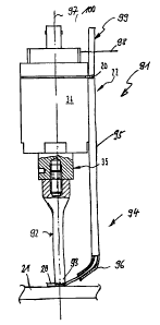
FIG. 3 shows the wiring device 22 in an individual representation with an
ultrasonic generator 34 which is arranged coaxially with respect to the wire
guide 23 and is rigidly connected to the latter in a connecting 'region 35.
Overall the wiring device 22 represented in FIG. 3 is of rotationally
symmetrical construction. The wire guide 23 comprises a central longitudinal
bore 36 which in the region of the wire-guide nozzle 30 merges with a wire
capillary 37 which in comparison with the longitudinal bore 36 has a narrowed
diameter that is matched to the diameter of the wire conductor 20. The wire-
guidance capillary 37 serves primarily to be able to align the wire conductor
exactly in the wiring plane 28 (FIG. 1 ).
In the embodiment example represented in FIG. 3 there are arranged to the side
of the wire guide 23, above the wire-guide nozzle and leading into the
longitudinal bore 36, two wire-feed channels 38, 39 which extend obliquely
downwards in the direction of the wire-guide nozzle 30. The wire-feed
channels 38, 39 serve for lateral introduction of the wire conductor 20 into
the
wire guide 23, so that the wire conductor 20, as represented in FIG. 3,
extends
laterally on a slant into the wire-feed channel 38, through the longitudinal
bore
36 and, guided out of the wire-guidance capillary 37, through the wire guide
23. In this case the multiple arrangement of the wire-feed channels 38, 39
permits selection of the wire-supply side of the wire guide 23 that is most
favourable in the given case.
As is further evident from FIG. 3, the wire-guide nozzle 30 is of convex
construction in the region of a wire outlet 40 in order to enable a deflection
of
the wire conductor 20 that is as non-damaging as possible in the region of the
19
CA 02449413 2003-12-11
contact point 32 (FIG. 1 ) or in the region of the wire outlet 40 in the
course of
the wiring operation represented in FIG. 1.
Although not represented in any detail in FIG. 3, the wire guide 23 may be
equipped with a wire-severing instrument and a wire-advancing instrument. In
this case the wire-severing device may be directly integrated into the wire-
guide nozzle 30. FIG. 4 shows a wire conductor 20 which, for the purpose of
forming a coil 41 which in this case takes the form of a high-frequency coil,
is
wired on a substrate 42. The coil 41 here has a substantially rectangular
configuration with an initial coil region 43 and a final coil region 44 which
are
guided away via a window-shaped substrate recess 45. In this case the initial
coil region 43 and the final coil region 44 are in parallel alignment with a
main
coil strand 46 which they accept between them in the region of the substrate
recess 45. In the course of the ultrasonic wiring of the wire conductor 20
already elucidated in principle with reference to FIG. 1 the ultrasonic
loading
of the wire conductor 20 is interrupted while the latter is being guided away
via
the substrate recess in the course of the wiring operation, in order on the
one
hand to ensure no impairment of the alignment of the wire conductor 20 in an
unrestrained region 47 between the recess edges 48, 49 located opposite one
another and on the other hand in order to rule out stressing of the connection
between the wire conductor 20 and the substrate 42 in the region of the recess
edges 48, 49 by tensile stresses on the wire conductor 20 as a consequence of
ultrasonic loading.
FIG. 5 shows, in a configuration that is modified in comparison with FIG. 4, a
coil 50 with an initial coil region 51 and a final coil region 52 which are
guided, angled in relation to a main coil strand 53, into an interior region
of the
coil S0. The coil 50 is arranged on a substrate 55 which comprises a substrate
recess 56 in the interior region 53 of the coil 50. In order to be able to
guide
away both the initial coil region 51 and the final coil region 52 via the
substrate
20
CA 02449413 2003-12-11
recess 56, in the case of the configuration represented in FIG. 5 the final
coil
region 52 has to be guided away beforehand in a crossing region 57 via the
main coil strand 44. In order in this case to prevent damage to or a partial
stripping of the wire conductor 20, similarly as in the region of the
substrate
recess 56 the ultrasonic loading of the wire conductor 20 is interrupted in
the
crossing region 57. Furthermore, the wire guide 23 is slightly raised in the
crossing region 57.
FIG. 6 shows, in a view of the substrate 55 corresponding to the course of the
line of intersection VI--VI in FIG. 5, the placement of a chip unit 58 in the
substrate recess 56, wherein terminal areas 59 of the chip unit 58 are caused
to
abut the initial coil region 51 and the final coil region 52.
FIG. 7 shows the subsequent connection of the terminal areas 59 of the chip
unit 58 to the initial coil region 51 and to the final coil region 52 by means
of a
thermode 60 which under the influence of pressure and temperature creates a
connection by material closure between the wire conductor 20 and the terminal
areas S9, as an overall result of which a card module 64 is formed.
In the case of the chip unit 58 represented in FIGS. 6 and 7 it may also be a
question, as in all other remaining cases where mention is made of a chip
unit,
either of an individual chip or of a chip module which, for instance,
comprises
a chip which is contacted on a chip substrate or even a plurality of chips.
Furthermore, the connection represented in FIGS. 6 and 7 between the coil 50
and the terminal areas 59 is not restricted to the connection to one chip but
applies generally to the connection of electronic components comprising
terminal areas 59 to the coil 50. In this case it may be also a question, for
example, of capacitors.
Furthermore, it becomes clear from FIGS. 6 and 7 that the substrate recess 56
is
21
CA 02449413 2003-12-11
so dimensioned that it substantially accepts the chip unit 58. With a view to
simplifying the alignment of the terminal areas 59 of the chip unit 58 in the
course of the placement of the chip unit 58 preceding the actual contacting,
the
chip unit 58 may be equipped on its contact side 61 comprising the terminal
areas 59 with an alignment aid 62 which here is constructed in the manner of a
bridge. The alignment aid 62 is dimensioned so as to correspond to the spacing
a which the initial coil region 51 and the final coil region 52 have from one
another in the region of the substrate recess 56 (FIG. 5).
FIG. 8 shows a production device 63 that serves for the manufacture of card
modules 64 that are used as semi-finished products in the manufacture of chip
cards. The card modules 64 manufactured by means of the production device
63 here have, by way of example, the structure represented in FIGS. 5, 6 and 7
with, in each instance, a coil 50 and a chip unit 58 arranged on a common
substrate 55.
The production device 63 represented in FIG. 8 comprises five stations, namely
a feed station 65, a wiring station 66; an assembly station 67 and a
connection
station 68 as well as an extraction station 69.
In the feed station there is supplied to the production device 63 a so-called
yield 70 which exhibits in a common composite a plurality of substrates SS--
here for representational reasons only twenty--which are connected to one
another via points of separation which are not represented here in any detail.
The yield 70 is supplied by means of a transport instrument 71 to the wiring
station 66 which comprises at a portal 73, which extends transversely in
relation to the production direction 72 and is capable of being displaced in
the
production direction 72, four identical wiring devices 22 arranged in a row.
The
wiring devices 22 are supplied with the wire conductor 20 via four wire-
conductor coils 74. For the purpose of forming the coil configurations
22
CA 02449413 2003-12-11
represented by way of example in FIG. 5, the wiring devices 22" which are
capable of being displaced along the portal 73, are displaced appropriately in
the wiring plane 28 (FIG. 1).
After wiring of the wire conductors 20 corresponding to the coil configuration
represented in FIG. S, the yield 70 with the coils 50 formed thereon is moved
on further to the assembly station 67. In the present case the connection
station
68 is combined with the assembly station 67 in such a way that, on a portal 75
which is capable of being displaced in the production direction 72, both an
assembly device 76 and a connecting device 77 are arranged so as to be capable
in each instance of being displaced in the longitudinal direction of the
portal
7S. In this case the assembly device 76 serves for extraction of chip units 58
from a chip-unit reservoir 78 and for subsequent placement of the chip units
58
in the manner represented in FIG. 6. The connecting device 77 serves to bring
the terminal areas 59 of the chip units 58 into contact with the coil 50, as
represented in FIG. 7.
After assembly and contacting, the yield 70 is moved on further into the
extraction station 69. Here an extraction of the yield 70 takes place with
subsequent separation of the substrates S5, or firstly a separation of the
substrates 55--that is to say, a dispersion of the composite yield--and
subsequently the extraction of the individual substrates SS which now take the
form of card modules 64.
FIG. 9 shows a particular application of the process elucidated by way of
example on the basis of FIG. 1 for the manufacture of a cylindrical formed
coil
79 wherein the substrate takes the form of a cylindrical winding support 80
and
the wiring or embedding of the wire conductor 20 on the winding support 80 is
effected in the course of rotation 81 of the winding support 80 with
simultaneous superimposed translation 82 of the wiring device 22.
23
CA 02449413 2003-12-11
As FIG. 10 shows, the winding support 80 may also take the form of a
cylindrical extension of a plastic vibrating diaphragm 83 of a loudspeaker
unit
84, so that in the manner represented in FIG. 9 a moving coil 85 is capable of
being manufactured such as serves, in combination with a permanent magnet
indicated in FIG. 10, to form a loudspeaker unit 84.
FIG. 11 shows, by way of another possible application of the process that has
been described, a ribbon-cable section 85 with a substrate 86 taking the form
of
a ribbon cable which, adjoined on both sides by points of separation 87, is
provided with substrate recesses 88 arranged in a row transverse to the
longitudinal direction of the substrate 86. On the substrate 86 there are
located,
arranged parallel to one another and extending in the longitudinal direction
of
the substrate 86, a plurality of wire conductors 20 which are wired on the
substrate 86 in the manner represented by way of example in FIG. 1. In this
case the wire conductors 20 are guided away in the region of the points of
separation 87 via the substrate recesses 88. The points of separation serve
for
the definition of predetermined ribbon-cable pieces 89, whereby the substrate
recesses 88 are then arranged in each instance at one end of a piece of ribbon
cable. In particularly favourable manner this results in contacting
possibilities
for connector plugs or connector sockets with the wire conductors 20 without
the wire conductors having firstly to be exposed for this purpose. The
substrate
recesses 88 are introduced into the substrate 86 in a stamping process with an
appropriately formed punch tool, whereby as a result of the spacing of the
stampings the spacing of the points of separation 87 is preset. Subsequently
the
appropriately prepared continuous substrate is covered with the wire
conductors 20, whereby in this case a number of wiring devices corresponding
to the number of wire conductors 20 are arranged above the substrate which is
moved longitudinally.
24
CA 02449413 2003-12-11
FIG. 12 shows, in a modification of the wiring device 22 represented in FIG.
3,
a wiring device 91 which, like the wiring device 22, comprises an ultrasonic
generator 34. As distinct ftom the wiring device 22, there is no wire guide
fastened to the connection region 35 of the ultrasonic generator 34 but rather
a
vibrating punch 92 which, as represented in FIG. 12, serves to subject the
wire
conductor 20 which is guided between a profiled end 93 and the surface of the
substrate 21 to the action of mechanical vibrations extending in the
longitudinal
direction of the vibrating punch 92 and induced by ultrasound. In order in
this
case to enable reliable guidance of the wire conductor 20, the profiled end 93
is
provided with a concave recess which is not represented in FIG. 12 in any
detail and which enables partial encompassing of the wire conductor 20.
As distinct from the wiring device 22 represented in FIG. 3, on the wiring
device 91 a wire guide 94 is provided which, in the case of the embodiment
example represented here, is formed from a guidance tube 95 arranged laterally
on the ultrasonic generator 34 with an elbow nozzle 96 which is formed in the
direction of the profiled end 93 and which enables lateral supply, here
directed
obliquely downwards, of the wire conductor 20 in the direction of the profiled
end 93. Hence, as represented in FIG. 12, the wire conductor 20 can be guided
between the profiled end 93 of the vibrating punch 92 and the surface of the
substrate 21 in order to enable the previously described connection to, or
alternatively wiring on, or in, the surface of the substrate 21.
Departing from the representation in FIG. 12, it is also possible to provide
the
wire guide on the wiring device 91, decoupled from the ultrasonic generator
34,
in order where necessary to enable vibration-free supply of the wire
conductor.
In the case of the embodiment example represented in FIG. 12 the wiring
device comprises a wire coil 99 which is capable of rotating about a winding
axis 98 arranged transverse to the punch axis 97 and which serves to supply
the
25
CA 02449413 2003-12-11
wire conductor 20 into the wire guide 95.
In order to enable arbitrary wiring of the wire conductor 20 on the surface of
the substrate 21, the wiring device 91 comprises, coaxially with respect to
the
punch axis 97, a pivotal axis 100.
In the language of the present patent application the terms "wire-shaped
conductor" and "wire conductor" generally designate conductors for the
transmission of signals that have a defined longitudinal extent and therefore
with respect to their external shape are of wire-shaped construction. However,
the term "wire conductor" is not restricted to metallic conductors but also
designates conductors made of other materials, for example light guides made
of glass fibre, or even conductors that serve for the guidance of flowing
media.
Particularly in the case where the conductors used are provided with an
adhesive surface it is also possible for the conductors to be disposed in
multiple
layers located on top of one another, the lowest layer being connected to the
surface of the substrate and other layers being connected in each instance to
conductor layers arranged below them. The adhesion may, for example, be
obtained via a coating of the conductor with baking lacquer which with regard
to its adhesive effect is capable of being activated by means of the action of
heat, or via an appropriate plastic coating.
FIG. 13 a card inlet pertaining to a chip card with a transponder unit formed
from a wire coil and a chip unit;
FIG. 14 a sectional representation of the card inlet represented in FIG. 13
according to the course of the line of intersection II--II, for the purpose of
elucidating the manufacturing process;
FIG. 15 another sectional representation of the card inlet represented in FIG.
13
26
CA 02449413 2003-12-11
according to the course of the line of intersection III--III;
FIG. 16 a representation corresponding in its view to FIG. 14 for the purpose
of
elucidating an alternative procedure with subsequent application of a chip
unit;
FIG. 17 the contacting of the chip unit applied subsequently according to FIG.
17;
FIG. 18 a possible contact metallisation of a terminal area of a chip with
contacting according to the process represented in FIG. 17;
FIG. 19 another possible contact metallisation of a terminal area of a chip;
FIG. 20 a representation corresponding in its view to FIG. 14 of a transponder
unit arranged on a coil substrate.
FIG. 13 shows a chip-card inlet 110 which, with a view to the manufacture of a
chip card by way of end product which is not represented in any detail here,
is
provided with bilateral surface layers which as a rule are applied onto the
chip-
card inlet in the form of laminated layers covering the surface.
The chip-card inlet 110 consists here of a coil substrate 111 formed from
plastic material, onto which a wire coil 112 is applied with the aid of wire-
laying technology. To this end a wire conductor 113 is wired on the surface of
the coil substrate 111 by means of a wiring instrument which is not
represented
in any detail in FIG. 13 and is partially embedded into the coil substrate 111
by
ultrasonic loading, as can be gathered from FIG. 14.
As is evident furthermore from the representation according to FIG. 13, in the
coil substrate 111 a recess 114 is provided which serves to accept a chip unit
27
CA 02449413 2003-12-11
constituted here by an individual chip 115. The chip unit may, as in the
present
case, be constituted merely by the chip 11 S. However, it is further possible
for
the chip unit to be formed from a so-called "chip module" which accepts one or
even several cased chips.
As is further evident from FIG. 13, the wire conductor 113 which is wired for
the purpose of forming the wire coil 112 on the coil substrate 111 is
contacted
with wire ends 116, 117 on an assigned terminal area 118 and 119,
respectively, of the chip 115.
A process for implementing the contacting of the wire ends 116, 117 with the
terminal areas 118, 119 of the chip 115 will be elucidated in more detail
below
with reference to FIG. 14. The process represented in detail in FIG. 14 is
effected in two successive phases, which here for the purpose of
differentiation
are denoted by I and II. In the phase designated by I the wire end 116
illustrated here is fixed on the coil substrate 111, whereby simultaneously as
a
consequence of the aforementioned wiring process for applying the wire
conductor 113 onto the surface of the coil substrate 111 the wire conductor
113
is guided away via the chip 11 S that is received in the recess 114. With a
view
to implementing the process represented in FIG. 14, the coil substrate 111 is
arranged on a table 120 together with the chip 11 S received in the recess
114.
By way of wiring instrument, in the case of the process example represented in
FIG. 14 use is made of an ultrasonic instrument 121 which with a vibrating
punch 122 embeds the wire conductor 113 which is continuously guided out of
a wire guide 123 into the surface of the coil substrate 111 and thereby
simultaneously executes a horizontal movement 124 on the surface of the coil
substrate 111. This application of the wire conductor 113 on the surface of
the
coil substrate 111, which is described by the term wirings, is firstly
effected in
the region designated by Ia to the left of the recess 114, subsequently the
wire
28
CA 02449413 2003-12-11
conductor 113 is guided away with the wire guide 123 via the chip 115 which
is arranged in the recess 114, in order finally to continue with the fixation
of
the wire conductor 113 on the right-hand side of the recess 114 in the region
headed by Ib by means of ultrasonic loading of the wire conductor via the
vibrating punch 122. Although when use is made of the ultrasonic instrument
121 described above for wiring the wire conductor 113 on the coil substrate
111 a fixation of said wire conductor arises extending substantially over the
entire length of the wire conductor 113 on the coil substrate 111, in order to
realise the principle of the process it is sufficient if a fixation of the
wire
conductor 113 on the coil substrate 111 is effected merely at two points to
the
left and right of the recess 114, in order to achieve the linear alignment of
the
wire conductor 113 represented in FIG. 14 via the terminal areas 118, 119 of
the chip 115.
After the wire conductor 113 is located in the position spanning the assigned
terminal area 118 of the chip 115, in the phase denoted by II the connection
of
the wire conductor 113 to the terminal area 118 is effected. To this end use
is
made, in the process example represented in FIG. 14, of another ultrasonic
instrument 125 which, as is evident in particular from FIG. 1 S, comprises a
profiled end 126 pertaining to a vibrating punch 127 and provided with a
concave recess.
The process described above with reference to FIGS. 14 and 15 also offers the
possibility, by appropriate choice of the points of fixation of the wire
conductor
on the substrate, of guiding the wire conductor away diagonally via the
terminal areas, in order to increase the overlap between the wire conductor
and
the terminal areas. Also, several chips or other elements arranged in series
on,
or in, a substrate can be connected by means of the wire conductor in the
manner represented in FIG. 14.
29
CA 02449413 2003-12-11
Furthermore, FIG. 15 shows clearly that, in contrast with the vibrational
loading 128 induced by ultrasound which is effected in the longitudinal
direction of the vibrating punch 122 of the ultrasonic instrument 121, the
vibrational loading 129 of the vibrating punch 127 induced by ultrasound is
effected transverse to the longitudinal direction of the wire conductor 113
and
parallel to the surface of the coil substrate 111. On this vibrational loading
128
a slight contact pressure 130 is superimposed, so that the wire conductor 113
which is received in guided manner in the profiled end 126 of the vibrating
punch 127 is moved back and forth in oscillating manner under pressure in the
region of the terminal area 118 above the latter. On the one hand this results
in
any oxide skins that may be present on the terminal area 118 being ripped open
and eroded, on the other hand a welding subsequently results, given
appropriately high or increased contact pressure 130, of the wire conductor
113, which here is formed from copper, to the aluminium terminal area 118. In
case the wire conductor 113 is provided with an external insulation the latter
can also be removed by the oscillating movement back and forth in the region
of the terminal area 118, so that subsequently the metallic connection
previously described between the wire conductor, which immediately
beforehand is still protected against oxidation by the insulation, and the
terminal area becomes possible.
In the coil substrate 111 represented in FIGS. 14 and 15 the recess 114 is
arranged so as to be larger than the corresponding dimensions of the chip 15,
so
that a circumferential gap 130 results between the chip 115 and the edges of
the
recess 114. By this means a virtually "floating acceptance" of the chip 115 in
the recess 114 is possible, whereby, although said chip is substantially
defined
in its location relative to the coil substrate 111, it is able to execute
minor
relative movements. This results in the advantage that, by virtue of the
laminating operation described in the introduction for application of the
bilateral surface layers onto the coil substrate 111, the chip can at least
partially
30
CA 02449413 2003-12-11
avoid the pressure loads associated with the laminating operation and
consequently the risk of damage to the chip in the course of the laminating
operation is significantly reduced.
In order also in the case of the "floating acceptance" of the chip in the
recess
114 described above to be able to carry out an exact positioning of the wire
conductor 113 on the terminal area 118, the wire conductor 113 can be tracked
via a corresponding transverse-movement axis 131 of the ultrasonic instrument
125.
Although with reference to the process example represented in FIGS. 14 and 15
two different ultrasonic instruments 121 and 125 were mentioned in the
foregoing description, there is also the possibility, given appropriate design
of
the ultrasonic instrument 121, of making use of the latter both for the wiring
and/or fixation of the wire conductor on the surface of the coil substrate 111
and for the connection of the wire conductor 113 to the respectively assigned
terminal area 118 or 119.
A way of proceeding that is slightly varied in comparison with FIGS. 14 and 15
is represented in FIGS. 16 and 17, wherein only after fixation of the wire
conductor 113 on the surface of the coil substrate 111 on both sides of the
recess 114 is a chip 132 introduced into said recess. In order simultaneously
with the introduction of the chip 132 into the recess 114 to enable a
positioning
that is suitable for the subsequent contacting of the wire conductor 113 with
an
assigned terminal area 133 of the chip 132, the latter is equipped on its
contact
side 134 with bridge-type alignment aids 135, in each instance arranged
adjacent to a terminal area 133, which provide for correct relative
positioning
via guide bevels 136.
FIG. 17 shows, in addition, a thermode instrument 137 which can be employed
31
CA 02449413 2004-07-22
as an alternative to the ultrasonic instrument 125 by way of a connecting
instrument which enables a connection of the wire conductor under pressure
and temperature loading to the assigned terminal area 133. With both of the
connection processes represented in FIGS. 14, 15 and 17 there is, in
principle,
the possibility of establishing the connection between the wire conductor and
the terminal areas by a superimposition of ultrasonic loading and temperature
loading, for example by means of a heatable ultrasonic instrument.
In order to enable a connection of the copper wire conductor 113 to the
aluminium terminal areas 133 of the chip 132, the terminal areas 133 are
provided with a contact metallisation 138 (FIG. 18) or 139 (FIG. 19). The
contact metallisations 138, 139 comprise, in corresponding manner, a zincate
layer serving as intermediate layer 140 which serves as foundation for a
nickel
layer 141 applied to it in the case of the contact metallisation 138, or a
palladium layer 142 in the case of the contact metallisation 139. With a view
to
improving the connecting capacity or with a view to increasing the oxidation
resistance, the nickel layer 141 is also provided with a gold coating 145. For
the purpose of clarifying the size dimensions, layer thicknesses of the layers
that are applied to the aluminium coating, about 1 to 2 pm in thickness, of
the terminal area 133 are given below by way of examples:
zincate layer: d = 150 nm;
nickel layer: d = 1-5 Vim;
palladium layer: d = 1-5 ~Cm;
gold coating: d = 100-150 nm.
FIG. 20 finally shows, in a variant of the representation according to FIG.
13,
the possibility of applying the process described above also for the direct
contacting of the wire conductor 113 with assigned terminal areas I I 8 and
119
of the chip 115 if the chip 115 is not arranged in a recess but rather on the
32
CA 02449413 2004-07-22
surface of a substrate 143. In the case of the substrate 143 represented in
FIG.
20 it may be a question, for example, of a paper substrate or of any other
substrate. Conforming with the process elucidated with reference to FIGS. 14
and 15, here too on both sides of an acceptance region or arrangement region
144 for the chip 115 a fixation is provided of the wire conductor 113 into the
surface regions of the substrate 143, here designated in simplified manner by
Ia
and Ib.
In particular on account of the particularly thinly formed substrate the
embodiment represented in FIG. 20 appears to be particularly suitable for use
as a transponder arrangement in connection with the identification of luggage.
Although in the foregoing embodiment examples reference is made, with a
view to elucidating the process, to transponder units consisting of a coreless
wire coil and a chip unit, use may of course also be made of ferrite-core
coils
such as are employed, for example, for the manufacture of animal transponders.
In any case, the chip or the chip unit can be made thinner prior to or after
the
application on, or in, the substrate, in order to-increase the flexibility of
the
chip and, where appropriate, to adapt the chip to the substrate as regards its
bending behaviour.
While specific embodiments of the invention have been shown and described
in detail to illustrate the application of the principles of the invention, it
will be
understood that the invention may be embodied otherwise without departing
from such principles. For example, the invention is generally applicable for
embedding a wire into a wiring plane of a substrate.
33