Note: Descriptions are shown in the official language in which they were submitted.
CA 02450014 2003-12-08
WO 02/100931 PCT/US02/17891
NANOCOMPOSITE DIELECTRICS
BACKGROUND OF THE INVENTION
1. Field of the Invention
The present invention relates to nanocomposite dielectrics of carbon
nanotubes,
high energy density capacitors of carbon nanotubes, and methods for increasing
the dielectric constant of a polymer matrix with nanocomposite dielectrics.
2. Description of the Background
Escalating requirements for size efficiency demanded by commercial and
military
for ground, medical, aircraft and space power systems demand reduced size for
components such as capacitors. Power loss of system components impedes size
reduction. Future requirements of system size and energy density demand stress
capability as well as dielectric constant of film dielectrics to be extended
to
higher ranges than currently available.
Several parameters are considered important factors for design and fabrication
of
advanced high energy density capacitors such as dielectric breakdown strength,
dielectric constant, and dissipation factor. For high energy density
capacitors, as
in all capacitors, the total stored energy per unit vohune is a function of
two key
properties of the dielectric, dielectric constant and the dielectric breakdown
strength. The total energy density is proportional to the square of the
dielectric
strength and linearly proportional to the dielectric constant, as shown below
in
equation 1: Energy Density (ED) = E2E/8~ wherein E is the dielectric constant,
and E is the operating electric stress.
Power density is proportional to voltage peak energy density times the AC
voltage frequency. Therefore, for high energy density capacitors, dissipation
factor should be kept to a minimum. One approach for increasing stored energy
density of a capacitor is to increase the capability of a dielectric to
withstand
higher peak voltage stresses. Key material properties for capacitor
dielectrics is
outlined below in Table 1.
CA 02450014 2003-12-08
WO 02/100931 PCT/US02/17891
2
Table 1: Key material properties for high energy density pulse
power capacitor dielectrics
Dielectric ' high, > 20,000 V/mil
breakdown
siren th
Dielectric Constant>4
Dissipation factor<3% for light duty (<~l/min.);
<1% for
medium rep rate
Consistency Roughness <5% of dielectric
thiclmess;
void free
Practicality Should be able to fabricate
into capacitors
by integration into current
production
methods at minimal cost and
investment
The ultimate energy storage in a capacitor varies by the square of the
operating
voltage; therefore doubling this voltage gives a four-fold increase in energy
storage. However, doubling the capacitance, by doubling the dielectric
constant,
only give a two-fold increase in energy storage.
Compact, high-temperature and high energy density (HED) capacitors have a
myriad of uses in both commercial and military applications. For example,
these
may be used with domestic utilities and appliances, well-drilling equipment,
power supplies, aircraft, satellites, trains, automobiles and medical devices.
The
high-temperature capability of the capacitors allows electronic devices to be
mounted close to aircraft engines. This permits more sophisticated engine
actuators, sensors and controls to be implemented with a net reduction in
weight
achieved through the reduction, or even elimination, of wiring hardware that
is
necessary when the electronics are remotely located. High-energy density
capacitors are also greatly needed for Air Force and Army pulse power
applications.
Y. Rao, J. Qu, C.P. along, IEEE Ti~ans. ore CPMT, 23, 680, Dec. 2000. briefly
reviewed the market need for integral decoupling capacitors (a.k.a., embedded
capacitance) for hand held devices and computers and predict that by 2004-
2006,
CA 02450014 2003-12-08
WO 02/100931 PCT/US02/17891
3
these applications will require Capacitance per unit area of 20 and 72 nF/cm2
respectively.
The standard relationship between Capacitance C and dielectric constant E,. is
as
follows:
S C= Eo E,.AIt
where
Eo dielectric constant of free space (8.8S4x10-12 F/m)
E,. dielectric constant of the inculator layer (dimensionless)
A area of the electrical conductor
t thickness of the insulator layer
According to this relationship, the dielectric constant of the insulator layer
should
be as high as 114 in order to achieve capacitance of 20 nF/cm2. Dielectric
constant values as high as 82 for composites comprising lead magnesium niobate-
lead titanate in an epoxy matrix have been demonstrated. Filler loadings as
high
1 S as 80 volume% were required, resulting in composites with poor mechanical
properties. Dielectric constants can be predicted for these types of
composites
using Effective-Medium Theory.
Accordingly, traditional approaches of filling high dielectric constant
fillers into a
polymer matrix require 80 volume % filler loading to achieve a composite
dielectric constant of 82. Thus, polymer-ceramic composites have practical
limits.
Furthermore. for miniaturized GPS adaptive antenna array applications, a
dielectric constant must be high enough to allow for sufficient size reduction
of a
patch antenna to fit their physical space requirements, which are four antenna
2S elements need to fit in a 3.S" square array aperture. If an artificial
dielectric with
CA 02450014 2003-12-08
WO 02/100931 PCT/US02/17891
4
a high enough dielectric constant was commercially available, it would be
directly applicable to this application.
(see:http://www.mitre.or~~pport/papers/tech~apers99 00/rao characterizing/r
ao characterizin~pdf)
Accordingly, a novel nanocomposite dielectric With a high dielectric constant
is
desired. A high energy density capacitor which can meet commercial and
military demands is also particularly desirable.
SUMMARY OF THE INVENTION
Accordingly, in a preferred embodiment, the invention provides a nanocomposite
dielectric comprising a polymer matrix and a plurality of carbon nanotubes
dispersed therein.
In another preferred embodiment, the invention provides a high energy density
(HED) capacitor comprising a polymer matrix and a plurality of carbon
nanotubes substantially dispersed therein.
In another preferred embodiment, the invention provides a circuit comprising a
high energy density (HED) capacitor of the instant invention.
In another preferred embodiment, the invention provides a method for
increasing
a dielectric constant of a polymer matrix, comprising dispersing a plurality
of
carbon nanotubes in said polymer matrix to form a nanocomposite dielectric and
measuring the dielectric constant of said nanocomposite dielectric.
In another preferred embodiment, the invention provides a laminate comprising
a
nanocomposite dielectric of the instant invention. Preferably, a metal layer
is
bonded to at least one side of the dielectric. Preferably, the laminate is
incorporated into a multilayer circuit structure to form an embedded
capacitor.
Preferably, the dielectric is reinforced with glass fabric. Preferably, the
dielectric
is greater than about 0.002 mrn thicl~.
CA 02450014 2003-12-08
WO 02/100931 PCT/US02/17891
In another preferred embodiment, the invention provides a mobile antenna
comprising a nanocomposite dielectric of the instant invention. Preferably, a
dielectric constant of said dielectric increases as size of said antenna
decreases.
Preferably, the plurality of carbon nanotubes are substantially single walled
5 carbon nanotubes.
Preferably, the plurality of carbon nanotubes are substantially rnulti-walled
carbon nanotubes.
Preferably, the plurality of carbon nanotubes are a mixture of single walled
and
multi-walled nanotubes.
Preferably, the polymer matrix is selected from the group consisting of epoxy
resins, cyanate ester resins, polyimides, silicones, polybutadiene resins,
fluoropolymers, urethanes, acrylics, polycarbonate, polypropylene,
polyethylene,
polyesters and mixtures thereof.
Preferably, the plurality of carbon nanotubes are oriented parallel to an
electric
field of the nanocomposite.
Preferably, a metal coating is deposited on the surface of said nanotubes to
increase conductivity of said nanotubes.
Preferably, the metallic coating is selected from the group consisting of
silver,
gold, copper, nickel, aluminum and mixtures thereof.
Preferably, .the nanotubes are present at a concentration below a percolation
threshold of said nanocomposite dielectric.
Preferably, the nanotubes are mixed with a conductive filler selected from the
group consisting of silver particles, nickel coated graphite, metallic coated
glass
beads, metallic coated hollow glass or ceramic spheres, copper particles,
stainless
steel fibers, carbon black, gold particles, aluminum particles and mixtures
thereof.
CA 02450014 2003-12-08
WO 02/100931 PCT/US02/17891
6
Preferably, the nanotubes are mixed with inorganic dielectric particles to
increase
the volume resistivity of said dielectric.
Preferably, an organic molecule is adsorbed or covalently bonded to a surface
of
said nanotubes to improve dispersion or increase the volume resistivity of
said
dielectric.
Preferably, the dielectric has a volume resistivity greater than about 10g ohm-
cm.
Preferably, the dielectric has a volume resistivity greater than about 1012
ohm-cm.
Preferably, the dielectric has a dielectric constant greater than about 4.
Preferably, the dielectric has a dielectric constant greater than about 10.
Preferably, the dielectric has a dielectric constant greater than about 40.
Preferably, the dielectric has a dielectric constant greater than about 100.
Preferably, the dielectric has a dielectric loss Iess than about 0.05.
Preferably, the
dielectric has a dielectric loss less than about 0.02.
Preferably, the dielectric has a dielectric breakdown strength greater than
about
1,000 volts/mil. Preferably, the dielectric has a dielectric breakdown
strength
greater than about 15,000 volts/mil. Preferably, the dielectric has a
dielectric
breakdown strength greater than about 20,000 volts/mil.shold of said
nanocomposite dielectric.
Additional objects, features and advantages of the invention will be set forth
in
the description which follows, and in part, will be obvious from the
description,
or may be learned by practice of the invention. The objects, features and
advantages of the invention may be realized and obtained by means of the
instrumentalities and combination particularly pointed out in the appended
claims.
CA 02450014 2003-12-08
WO 02/100931 PCT/US02/17891
7
BRIEF DESCRIPTION OF THE DRAWINGS
Fox a more complete understanding of the present invention, the objects and
advantages thereof, reference is now made to the following descriptions taken
in
connection with the accompanying drawings in which:
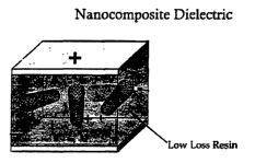
Fig. 1 depicts a HED Capacitor based on a nanocomposite dielectric according
to
one embodiment of the present invention;
Fig. 2 depicts calculations of Kc for SWCNT of several lengths below
percolation
according to one embodiment of the present invention;
Fig. 3 depicts a plot of dielectric constant versus concentration of nanotubes
in
resin according to one embodiment of the present invention;
Fig. 4 depicts a plot of dielectric constant (El) and loss (E2) versus reduced
frequency according to one embodiment of the present invention;
Fig. 5 depicts experimental measurements of Kc as a function of frequency for
carbon nanotubes suspended in water according to one embodiment of the present
invention;
Fig. 6 depicts known carbon nanotubes;
Fig. 7 depicts a SEM of SWCNT, including ropes and particles of catalyst and
amorphous carbon;
DETAILED DESCRIPTION OF PREFERRED EMBODIMENTS
Maximum energy density is a result of a combination of increased dielectric
constant and higher voltage stress. In reality, a dielectric constant is not a
constant, but is rather a time/frequency dependent dielectric relaxation (see
D.A.
Seanor, Electrical Properties of Polymers, Academic Press, Inc., D 1982).
Thus,
a highly polarized response to changing electric fields should be on a time
scale
siguficantly faster than the desired time scale of energy discharge for the
capacitor in order to be a useful high dielectric constant. The novel
CA 02450014 2003-12-08
WO 02/100931 PCT/US02/17891
g
nanocomposite dielectric of the present invention has a dielectric constant
that
results from both an dielectric constant of a polymer matrix and the
instantaneous
polarization of carbon nanotubes dispersed therein. Preferably, the nanotubes
are
dispersed substantially uniformly in the polymer matrix.
Y. Rao, C.P. Wong, "Ultra High K Polymer Based Composite for Embedded
Capacitor Application", demonstrated that dielectric constants as high as
1,000
can be achieved by using conductive fillers dispersed in an epoxy matrix. This
was achieved at ~11 volume% filler loading. The dielectric loss for this
composite was also moderately low at 0.019. The dielectric properties were
measured at relatively low frequency (10 kHz), so loss would likely be much
higher at microwave frequencies (1 GHz and higher). This reference clearly
validates an artificial dielectric approach to trying to achieve embedded
capacitance in next generation electronic products.
The instant invention is advantageous over conventional artificial dielectric
approaches with regard to cost, ease of processing and mechanical properties.
The instant invention operates in a much lower filler loading range, which
minimizes negative impact on processing since lower viscosity should be
possible and mechanical properties such as higher strength and higher
ductility
should be possible.
The selection of the polymer matrix is not critical. In general, any polymer
can
be used which is a dielectric and can uniformly disperse carbon nanotubes. The
specific application will generally dictate which polymer matrix is used. For
example, for circuit board or wiring board applications, a polymer matrix is
preferably selected from an epoxy fiberglass resin. Selection of the polymer
matrix is well within the skill of the skilled worker and within the scope of
the
invention.
The polymer matrix may comprises a polymer selected from one or more of the
materials commonly used for electronics packaging, including, but not limited
to
epoxy resins, cyanate ester resins, polyimides, silicones, polybutadiene
resins,
CA 02450014 2003-12-08
WO 02/100931 PCT/US02/17891
9
fluoropolymers, urethanes, acrylics, polycarbonate, polypropylene,
polyethylene,
polyesters and combinations thereof.
Indeed, the recent discovery of carbon nanotubes offers new possibilities to
modify the electrical properties of the polymer matrix system. Carbon
nanotubes
are a highly ordered, high aspect ratio, forms of carbon with extreme
mechanical,
electrical, and thermal properties. Their integration into nanocomposites for
electronics will lead to the next generation capacitors.
Although only first widely reported in 1991 , carbon nanotubes are now readily
synthesized in gram quantities. Carbon nanotubes are essentially single
graphite
layers wrapped into tubes that exist as either single walled (SWCNT) or multi-
walled (MWNT) wrapped in several concentric layers, as shown in Fig. 6.
SWCNTs are composed of a single wall of hexagonally bonded graphene sheet
(graphite is made of graphene sheets stacked like pancakes). Like the
archetypal
fullerene, C6o, they divide space into two volumes, an inside and an outside,
separated by a chemically robust, one-atom thick, impermeable membrane. The
perfection of the bonding of this graphene membrane gives such fullerene
carbon
nanotubes outstanding properties, including: electrical conduction equivalent
to
metals like copper and gold; thermal conductivity along the tube axis equal to
or
better than that of any other material; a tensile strength expected to be
higher than
any other material; 30-100 times higher strength than steel at one-sixth the
weight; and extreme stiffness combined with ability to withstand repeated
bending, buckling, twisting, and/or compression at high rates with complete
elasticity.
Carbon nanotubes have three major assets for potential technological
applications: (1) electrical properties; (2) thermal properties; and (3)
extremely
high mechanical strength.
Wetting of multiwall and single wall carbon nanotubes is common in the art.
Wetting of nanotubes is a criterion for dispersion. One material will "wet
out"
another material if the resulting surface tension at the interface of the two
CA 02450014 2003-12-08
WO 02/100931 PCT/US02/17891
materials is below the critical surface tension for wetting the dispersed
material.
Most organic compounds and resin systems wet both single and multi-walled
nanotubes. Most cormnon organic solvents, monomers, and pharmaceuticals will
even wet into the hollow interior of nanotubes.
5 In a preferred embodiment, a metallic coating is added to the surface of the
nanotubes to increase the conductivity of the nanotubes. The metallic coating
may be selected from any metal commonly used as conductors in electronics
packaging, including, but not limited to silver, gold, copper, nickel, and
aluminum. For example, U.S. Patent No. 6,013,206 discusses a process for
10 synthesizing lipid tubules and coating the tubules with metal to render
them
conductive. The tubules are microscopic . hollow cylinders that self assemble
from lipids. Typical dimensions are ~ O.S~,m diameter and L/D 100. Without
the metallic coating, the lipid tubules are non-conductive. By mixing these
metallized tubules at very high loadings with polymers, they were able to
produce
polymer composites with interesting dielectric properties. The metallized
tubules
at high loading densities in composites develop very high dielectric
responses,
which allow microwave energy to be guided and absorbed, which is a very useful
property in the aerospace industry. Applications of interest to this research
group
are radar absorbing materials and color-based biosensors.
Accordingly, nanocomposite dielectrics comprising carbon nanotubes in a
polymer matrix are enhanced by metallizing the carbon nanotubes. The metallic
coating will render nanotubes more conductive, thereby making it possible to
achieve even higher dielectric constant than when non-metallized nanotubes are
used. These composites should have advantages over the metallized lipid
tubules
due to geometric considerations. For example, nanotubes are much smaller in
diameter, such as ~ lnm, and have a much lugher aspect ratio (>1,000), and
conductivity considerations since nanotubes are intrinsically electrically
conductive prior to metallization.
In another preferred embodiment, the nanotubes are oriented by exposing the
films to a shearing, stretching, or elongating step or the like, e.g., using
CA 02450014 2003-12-08
WO 02/100931 PCT/US02/17891
11
conventional polymer processing methodology. Such shearing-type processing
refers to the use of force to induce flow or shear into the film, forcing a
spacing,
alignment, reorientation, disentangling of the nanotubes from each other
greater
than that achieved for nanotubes simply formulated either by themselves or in
admixture with polymeric materials. Oriented nanotubes are discussed, for
example in U.S. Patent No. 6,265,466, which is incorporated herein by
reference
in its entirety. Such disentanglement can be achieved by extrusion techniques,
application of pressure more or less parallel to a surface of the composite,
or
application and differential force to different surfaces thereof, e.g., by
shearing
treatment by pulling of an extruded plaque at a variable but controlled rate
to
control the amount of shear and elongation applied to the extruded plaque.
Oriented refers to the axial direction of the nanotubes. The benefits of
orientation
are discussed, for example, in "The permittivity at X-band frequencies of
nickel-
coated graphite fibers in an epoxy matrix," Y.-S. Ho and P. Schoen, J. Matl.
Research, 9, 246-251 (1994), wherein the authors demonstrate nickel-coated
graphite fibers dispersed in an epoxy matrix and leads to composites with high
dielectric constant. Dielectric constants as high as 75 are achieved, compared
with a value of 2.8 for the unfilled epoxy. Fiber orientation parallel to the
electric
field is demonstrated by showing a maximum possible fiber loading for fibers
oriented perpendicular to the electric field exhibited dielectric constants
less than
half that of those composites comprising fibers oriented parallel to the
electric
f eld. Lastly, the reference discusses benefits of adding a non-conductive
inorganic filler to the system to facilitate dispersion and serve as a
physical
barrier preventing fibers from coming into physical contact. The resulting
composites exhibited lower dielectric loss than composites without the fumed
silica.
Preferably, the nanotubes are oriented parallel to the electric field. This
type of
orientation is advantageous since carbon nanotubes have a high aspect ratio
compared with fibers used by the prior art since nanotubes have an aspect
ration
of greater than 1,000, whereas the aspect ratio fox prior art nickel-coated
graphite
fibers is 100 or less. High dielectric constants are realized with a carbon
filled
CA 02450014 2003-12-08
WO 02/100931 PCT/US02/17891
12
polyner composite with low dielectric loss. The higher dielectric constant may
be due to geometric considerations, such as a smaller diameter and much higher
aspect ratio.
The instant inventors have discovered that suspending elongated, conducting
obj ects, such as carbon nanotubes within the matrix, enhances the dielectric
constant of insulating matrix material, such as plastic. The polarizability of
the
conducting nanotubes enhance the dielectric constant of the composite, Kc. If
the
volume-filling fraction of the objects is too high, however, the conducting
objects
begin to touch, thereby forming conducting paths within the volume of the
matrix, a process known as percolation. Percolation materials have significant
values of bulk electrical conductivity, and therefore can be used for
electrostatic
discharge or electromagnetic-shielding applications. They generally cannot,
however, be used to make capacitors because their losses are too high. The
loss
is given by the loss tangent: tan8 = Kc"/KC' which is preferably low enough
for
capacitor applications.
In the context of the instant invention, the amount of carbon nanotubes added
to
the polymer is such that the instant dielectric has a dielectric loss
preferably less
than or equal to 0.05 for capacitor applications. More preferably, the instant
dielectric has a dielectric loss less than about 0.02.
In a preferred embodiment, an organic molecule is adsorbed or covalently
bonded
to a surface of said nanotubes to improve dispersion or increase the volume
resistivity of said dielectric.
In a preferred embodiment, the instant dielectric has a volume resistivity
greater
than about 10' ohm-cm, and preferably greater than about 109 ohm-cm. More
preferably, the volume resistivity greater than about 1012 ohm-cm.
In a preferred embodiment, the instant dielectric has a dielectric constant
greater
than about 4. More preferably, the dielectric has a dielectric constant
greater than
about 10. Even more preferably, the dielectric has a dielectric constant
greater
CA 02450014 2003-12-08
WO 02/100931 PCT/US02/17891
13
than about 40. Even more preferably still, the dielectric has a dielectric
constant
greater than about 100.
In a preferred embodiment, the dielectric has a dielectric breakdown strength
greater than about 1,000 volts/mil. More preferably, the dielectric has a
dielectric
breakdown strength greater than about 15,000 volts/mil. Even more preferably,
the dielectric has a dielectric breakdown strength greater than about 20,000
volts/mil.
In a preferred embodiment nanotubes are mixed With a conductive fillers
selected
from one or more materials commonly used for electronics packaging, including,
but not limited to silver particles, nickel coated graphite, metallic coated
glass
beads, metallic coated hollow glass or ceramic spheres, copper particles,
stainless
steel fibers, carbon black, gold particles, aluminum particles.
In another preferred embodiment, the invention provides a laminate comprising
a
nanocomposite dielectric of instant invention. Ina preferred embodiment a
metal
layer, such as copper foil, is bonded to at least one side of the dielectric.
The
laminate may be incorporated into a multilayer circuit structure to form an
embedded capacitor. Preferably, the dielectric is reinforced with glass fabric
and
is greater than about 0.002 mm thick.
There remains an increased need for high-dielectric constant materials for the
development of miniaturized antennas for mobile communications such as mobile
phones, GPS and bluetooth communications systems.
Accordingly, in another preferred embodiment, the instant invention provides a
mobile antenna comprising a nanocomposite dielectric of the instant invention.
Preferably, the dielectric constant of the dielectric increases as size of
said
antenna decreases, based on antenna theory, the design width of a antenna is
given by:
W = (1 / 2fr (~oEO)v2) (2 / (ET + 1)) lie
where
CA 02450014 2003-12-08
WO 02/100931 PCT/US02/17891
14
f,. Operating frequency fox the antenna (or resonant frequency);
,uo and Eo Fundamental physical constants;
E,. Dielectric constant of the substrate.
Accordingly, the width of the antenna is inversely proportional to the square
root
of the dielectric constant. Similarly, the length of the patch antenna also is
inversely proportional to the square root of the dielectric constant.
Therefore, a
dielectric constant of 100 should result in a (100/10)12 or > 3-fold reduction
in
both length and width of the antenna compared with a dielectric constant of 10
(alumina substrate). This would translate into an area (L x W) reduction of 10
fold. See: Garg, Ramesh; Bhartia, Prakash; Bahl, Inde; Tttipiboon, Apisack;
Microstrip Antenna Design Handbook, Artech House, Inc. 2001.
The preferred embodiment of the present invention and its advantages are best
understood by referring to the Figures of the drawings, like numerals being
used
for like and corresponding parts of the various drawings. In this corniection,
a
schematic of a nanocomposite dielectric according to one embodiment of the
present invention is depicted in Fig. 1.
According to another embodiment of the present invention, a method for
producing dielectric films is provides. Purified carbon nanotubes are
compounded into a desired polymer, cast into films, oriented, metallized, and
tested.
In a preferred embodiment, the addition of carbon nanotubes to the polymer
host
is carefully controlled to provide a uniformly dispersed nanocomposite with a
concentration of nanotubes below the percolation threshold. Some samples of
the
instant nanocomposite may be formed in thicker preparations to facilitate lugh
frequency testing. These films may be characterized for electrical,
morphological, and thermal properties.
In general, to prepare a nanocomposite resin, two steps are followed: 1) the
acquisition of carbon nanotubes and characterization, and 2) the dispersion of
the
CA 02450014 2003-12-08
WO 02/100931 PCT/US02/17891
1S
tubes into one or more resins for use in fabrication thin films and monolithic
solids for testing. Each of these steps is discussed herein.
Nanotubes may come in many conductivities, purities, length distributions,
diameters distributions, and axe delivered in numerous forms, such as being
suspended in toluene as a slurry. It is this variability in the sources of
nanotubes,
which requires some degree of internal testing to characterize the basic
properties.
In order to characterize the nanotubes, they are viewed under SEM and TEM to
assess the diameters, lengths and purity, see Fig. 7. Some synthetic processes
yield nanotubes with by-product, such as an HiPCO process, which may result in
metal catalyst at a loading of 2-4% and may have some amount of amorphous
caxbon.
The nanotubes may be dispersed in a solvent of resins. Prevention of
flocculation
of the tubes to form ropes is desirable as shown in Figure 9. Preferably, an
I S aprotic organic solvent is used, such as NMP, DMAC, or DMSO, which form
stable suspensions lasting several hours, which is long enough to cast films.
The
selection of polymer resin host is less important than the forming a mliform
dispersion.
Compounding is performed by either ultrasonic or high shear mixing techniques.
A range of nanotube loading levels may be prepared. Solutions may be
monitored by an optical microscope to determine aggregation. The resulting
solutions may be used as is for electrical measurements at high frequency.
Capacitors may be formed by casting films, forming monoliths, and metal
coating. The resulting capacitors and bulk pieces may be characterized for
dielectric properties and quality of dispersion by imicroscopy. In this
connection,
the invention also encompasses circuits, circuit boards or wire boaxds
comprising
the instant nanocomposite dielectric materials.
CA 02450014 2003-12-08
WO 02/100931 PCT/US02/17891
16
Film casting may be performed in specialized dishes, using doctor blades. By
controlling the cast thickness, concentration of the resin, and environment
around
the cast resin, drying is uniform and results in excellent films. These films
may
be made very thin by using dilute solutions. Thick parts may be formed by
layering films and vacuumed pressing the thermoplastic sheets together to form
a
solid.
The films may be sputter-coated with gold to form electrodes for measuring
dielectric constant, and loss factor. Break-down strength can be determined
with
or without electrodes.
Measuring high-frequency complex dielectric constants (0.2-20 GHz), may be
preformed with the following equipment: (1) HP 85070B dielectric probe; and
(2) HP 8720C network analyzer. For measuring low-frequency complex
dielectric constant (5 Hz-13 MHz), may be preformed with the following
equipment: (1) HP 16451B dielectric test fixture; and (2) HP 4192A LF
impedance analyzer.
Breakdown testing is a bulk material property that is dependent on test
apparatus
and conditions like humidity. Therefore, breakdown testing is performed to all
samples and control samples in series on the same day to reduce day-to-day
variability. In this way, a reference value for comparison may be provided.
For a high-energy density capacitor, the dielectric constant, loss factor, and
operational voltage all determine the end use and ultimate storage capacity.
Of
these three, the most important may be operating voltage. The energy stored in
a
capacitor is calculated from the following expression:
W(j)-C~V2
where:
W is in joules
C is capacitance in Farads, and
CA 02450014 2003-12-08
WO 02/100931 PCT/US02/17891
17
V is Volts.
The dielectric properties of the nanocomposite may be tested under various
conditions, ranging from static to high frequency conditions. According to one
embodiment of the present invention, the addition of nanotubes to the polymer
host is carefully controlled to provide a uniformly dispersed nanocomposite
with
concentration of nanotubes below the percolation threshold as discussed
herein.
The thickness of the instant composites may be varied in order to facilitate
high
frequency testing. The films may be characterized for electrical,
morphological,
and thermal properties. The dielectric system provides very unique electrical
properties with a greatly enhanced dielectric constant. In this way, the
invention
provides a new generation of capacitor dielectric materials that demonstrate
that
the addition of a nanoscopic highly conductive, high aspect ratio particles to
a
high breakdown strength, low loss polymer host greatly enhances the dielectric
constant without increasing loss or decreasing breakdown strength.
For decades, materials scientist and engineers have been exhaustively
exploring
all forms of materials for use in capacitors. Enormous strides toward
improving
the energy storage capability have already been attained. However, in the
context
of HED capacitors, new weapons systems require energy storage and delivery at
unprecedented magnitudes.
In another preferred embodiment, the invention provides a next generation of
HED capacitors comprising a nanocomposite materials to exploit synergistic
contributions between established high performance bulk dielectric materials
and
non-intuitive engineering of materials with unique properties at the nano-
scale.
In this regard the invention provides an HED capacitor comprising a
nanocomposite dielectric material comprising a polymer matrix having a
plurality
of carbon nanotubes dispersed substantially uniformly therein.
Fig. 2 shows the results of effective-medium calculations of Kc for single-
wall
metallic carbon nanotubes of several lengths below percolation. Fig. 2 shows
that Kc can be greatly enhanced for large values of nanotube aspect ratio
CA 02450014 2003-12-08
WO 02/100931 PCT/US02/17891
1~
(length/radius). This figure also shows that, for example, tan8 is less than
0.01 at
frequencies less than 10 MHz for nanotubes that are 10 pm long and that have a
resistivity of 30 p,S~ ~cm. Other calculations show that the upper frequency
at
which tan8 = 0.01 can be increased by decreasing the nanotube resistivity.
As discussed above, nanotube concentrations above the percolation threshold, a
dielectric loss factor can be incorporated by adjusting the nanotube
concentration.
Below this concentration, known as the percolation threshold, nanotube
composites are nonconductive, but have a high dielectric constant. Both the
dielectric constant and the loss tangent, the two parameters that make up the
loss
factor, can be adjusted.
The dielectric response of nanotube composites is quite different from that of
composites with spherical inclusions, even at small concentrations. The
difference is possible due to long-range correlations in the interaction of
the
nanotubes. This long-range interaction is a distinct feature of high aspect
ratio
conductive fillers, while for spherical paxticle they are negligible.
The instant nanocomposites demonstrate low percolation thresholds since
nanotubes have a much lower percolation threshold than typical fillers due to
their high aspect ratio of >1000 and their high conductivity. For example, the
calculated percolation threshold for carbon black is 4%, while the threshold
is
below 0.04%, or two orders of magnitude lower, for typical caxbon nanotubes. A
high aspect ratio of carbon nanotube affords a filler loading level far lower
than
that of any other composite.
Refernng to Fig. 3, the effective dielectric constant and dielectric loss for
the
nanotube filled layer increases dramatically near the percolation threshold
and is
lower at nanotube concentrations above or below this critical value (Pc).
Further,
the dielectric loss factor for a nanotube-filled resin as a function of
concentration
behaves similarly to that of the dielectric constant, increasing in value up
to
percolation threshold. These results are dependant on the aspect ratio and
homogeneity of the nanotube within the composite.
CA 02450014 2003-12-08
WO 02/100931 PCT/US02/17891
19
In addition, refernng to Fig. 4, the loss factor is frequency dependant. This
figure
depicts the dielectric constant and loss as a function dimensionless
frequency.
The concentration of the nanotube is 10% of that required to reach the
percolation
threshold. The data peaks at the resonance frequency of the nanotubes. The
resonance frequency is length dependant. By selecting the correct
concentration
and length of nanotubes, a nanocomposite-resin for controlled behavior at a
variety of frequencies can be produced.
Fig. 5 shows experimental measurements of Kc as a function of frequency for
carbon nanotubes suspended in water. This data was taken at slightly below the
percolation threshold. At ~50 MHz, the nanotubes increase Kc' by a factor of
~4
over that of pure water, although tan8 ~0.5 at this frequency, may be too high
for
capacitor applications. However, these results demonstrate the potential of
carbon nanotubes to enhance the dielectric constants of materials, such as a
polymer, that can be used to make HED capacitors.
The complex relative dielectric constant was calculated for a composite made
of
metallic single-wall carbon nanotubes suspended in lossless matrix with a
relative
dielectric constant of 2.0, close to that of many plastics. The volume filling
fraction was 1 ~ 10-5. The nanotube resistivity and collisional relaxation
time
were 30 ~,Wcm and 1.4 ~ 1O-12 s, respectively. For these calculations, it is
assumed that the nanotubes have the dimensions of a (10,10) nanotube, the
dimensions of the nanotubes commonly found. In this plot "kr" is the real part
of
the composite's complex dielectric constant, and "ki" is the imaginary part
(see
also Fig. 2).
The complex relative dielectric constant measured with ("nt") and without
("neat") single-wall carbon nanotubes suspended in water using a surfactant.
The
weight fraction of the nanotubes was 0.681 rng/ml, corresponding to a volume
filling fraction of ~2 ~ 10~. Tt appears that this data was taken at slightly
below
the percolation threshold. These plots show the ability of carbon nanotubes to
enhance the dielectric constant of the matrix material. In this f gore, k' is
the real
part of the complex relative dielectric constant and k" is the imaginary part.
CA 02450014 2003-12-08
WO 02/100931 PCT/US02/17891
Although only a few exemplary embodiments of the present invention have been
described in detail in this disclosure, those skilled in the art who review
this
disclosure will readily appreciate that many modifications are possible in the
exemplary embodiments (such as variations in sizes, structures, shapes and
5 proportions of the various elements, values of parameters, or use of
materials)
without materially departing from the novel teachings and advantages of the
invention. Accordingly, all such modifications are intended to be included
within
the scope of the invention as defined in the appended claims. Other
substitutions,
rmodifications, changes and omissions may be made in the design, operating
10 conditions and arrangement of the preferred embodiments without departing
from
the spirit of the invention as expressed in the appended claims.
Additional advantages, features and modifications will readily occur to those
skilled in the art. Therefore, the invention in its broader aspects is not
limited to
the specific details, and representative devices, shown and described herein.
15 Accordingly, various modifications may be made without departing from the
spirit or scope of the general inventive concept as defined bye the appended
claims and their equivalents.
As used herein and in the following claims, articles such as "the", "a" and
"an"
can connote the singular or plural.
20 All documents referred to herein are specifically incorporated herein by
reference
in their entireties.