Note: Descriptions are shown in the official language in which they were submitted.
CA 02450143 2003-12-08
WO 02/101601 PCT/US02/18424
REPRESENTING THE DESIGN OF A SUB-MODULE IN A
HIERARCHICAL INTEGRATED CIRCUIT DESIGN AND ANALYSIS SYSTEM
BACKGROUND
I. Field of the Invention
The invention is related to electronic circuit fabrication. More particularly,
the invention is
related to systems for designing and verifying the contents and layout of an
integrated circuit.
2. Related Art
In Electronic Computer Aided Design (ECAD) software systems, an integrated
circuit design
specification and implementation data must be stored as a set of database
records, and these records
have some finite maximum size based on the virtual memory capacity of the
computer on which the
software is running. In addition, the execution time of the ECAD software
normally increases with
the size of the design. The data to represent a very large integrated circuit
design may be too large to'
fit in a computer's memory, or the execution time required to design or
simulate the entire design may
be prohibitive. This is particularly true where the number of components (i.e.
gates) and attendant
connections within an integrated circuit are in the lOs or 100s of millions or
more.
Hierarchical decomposition or "partitioning" is a technique which may be used
to reduce the
complexity of a large integrated circuit design specification so that the
memory and/or execution time
required to complete the design remains manageable. Instead of representing
the design as a single
flat database, the design is partitioned into pieces, often called "blocks",
which can be designed and
verified independently. With a given single level of hierarchy, the design
specification consists of a
set of blocks and the top-level interconnections between those blocks. With
multiple levels of
hierarchy the blocks may themselves consist of smaller sub-blocks and their
interconnections.
Hierarchical decomposition may also be used simply as an organizational tool
by a design
team as a method for partitioning a design project among several designers.
However, this logical
hierarchy created by the design team in the design specification does not need
to be the same as the
physical hierarchy used to partition the design for implementation. Often the
logical hierarchy is
CA 02450143 2003-12-08
WO 02/101601 PCT/US02/18424
much deeper than the physical hierarchy. A process of block flattening may be
used to transform the
logical hierarchy into an appropriate physical hierarchy.
A conventional hierarchical design project typically proceeds in two major
steps: a top-down
block planning step followed by a bottom-up verification step. If the blocks
themselves are
implemented during the top-down phase (i.e. each block is implemented before
its children) the flow
is referred to as a top-down flow. Conversely, if the blocks are implemented
during the bottom-up
phase (i.e. each block is implemented after all of its children have been
completed) the flow is
referred to as a bottom-up flow. The top-down and bottom-up flows each have
their advantages and
disadvantages. Without loss of generality, a top-down flow is used as an
example in the remainder of
this document. A bottom-up flow could be implemented using identical
techniques.
Figure 1 shows a typical top-down block planning and implementation flow. It
begins with a
partitioning of the design netlist to map the logical hierarchy into the
physical hierarchy, defining the
top-level block and the set of sub-blocks to be implemented (step 110). Each
sub-block is then
assigned a width and height value and a placement in the floorplan (step I
15). Locations are then
assigned to the pins on each sub-block, which represent the locations where
nets cross the sub-block
boundaries (step 120). This is followed by a time budgeting step that assigns
signal arnval/required
time constraints to each sub-block pin, indicating which portion of the clock
cycle is allocated to the
timing paths that cross the sub-block boundaries (step 135).
At this point in a top-down flow, after the top-level block has been planned,
the process is
prepared to implement the block. A11 Leaf cells (standard cells and macros)
owned by the block are
assigned a placement, and all nets owned by the block are routed (step 140).
If any of the nets were
routed over the sub-blocks (so-called "feedthrough nets") these wires are
pushed down into the sub-
blocks that they overlap, and new pins are created on the sub-block where the
wires cross the sub-
block Boundaries (step 145). Then, recursively implement the sub-blocks
according to the same
process (step 150). This involves recursively performing steps 110 to 170
while treating each sub-
block as the top-Ievel block.
For the above process to complete successfully the shapes, pin locations, and
timing budgets
assigned to each block (steps 115 through 135) must represent achievable
constraints. Otherwise the
CA 02450143 2003-12-08
WO 02/101601 PCT/US02/18424
system may not be able to complete the implementation of some blocks according
to their
specifications. In such a case the speciftcations may need to be refined and
the top-down process may
need to be repeated before a correct implementation can be realized. Such an
iterative refinement is
time-consuming and should be avoided. Thus, methods for achieving high-quality
results in these
steps are of critical importance.
When the recursive top-down planning and implementation step is complete the
bottom-up
verification process can commence. Proceeding from the lowest-level blocks
toward the top-level,
each block is independently analyzed for logical correctness, as well as its
timing and electrical
performance, and compared against its specification (step 155). After all sub-
blocks of a block have
been independently verified the block itself can be analyzed (step 170), under
the assumption that the
sub-blocks are correct.
SUMMARY OF THE INVENTION
In various embodiments, the invention consists of the creation and use of a
reduced model,
referred to as a block "abstraction", that captures the structure and behavior
of the block in sufficient
detail that the interface with its parent block and its sibling blocks may be
correctly analyzed. The
goal of the abstraction is to reduce the amount of memory required to
represent a block to its
ancestors in the hierarchy, and reduce the amount of execution time required
to analyze each instance
of the block in the context of its parents and sibling blocks.
BRIEF DESCRIPTION OF THE DRAWINGS
These and other objects, features and advantages of the present invention are
better
understood by reading the following detailed description, taken in conjunction
with the accompanying
drawings, in which:
Figure 1 shows a typical top-down block planning and implementation flow;
Figure 2 illustrates a hierarchical design process according to one or more
embodiments of
the invention;
Figure 3 illustrates the abstraction process according to at least one
embodiment of the
invention;
CA 02450143 2003-12-08
WO 02/101601 PCT/US02/18424
Figure 4 illustrates the logical shell labeling process according to at least
one embodiment of
the invention;
Figure 5 illustrates a block which undergoes this labeling process;
Figure 6 summarizes the process data inputs step of Figure 4;
Figure 7 summarizes the process pin forward step shown in Figure 6;
Figure 8 summarizes the process outputs step of Figure 4;
Figure 9 summarizes the process pin backward step shown in Figure 8;
Figure 10 summarizes the process clock inputs step of Figure 4;
Figure 11 summarizes the process clock pin forward step shown in Figure 10;
Figure 12 shows the physical timing shell model in an embodiment of the
invention; and
Figure 13 illustrates an exemplary computer system capable of implementing and
applying
one or more embodiments of the invention.
DETAILED DESCRTPTION
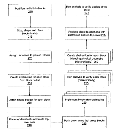
One way of implementing the top-down hierarchical design process is the
hierarchical design
flow shown and described in Figure 2. The design flow shown in Figure 2 is a
refinement of the top
down flow shown in Figure 1, with three additional steps, 230, 260, and 265.
The refinement
concerns a method for modeling a sub-block, in the context of its parent and
sibling blocks, during the
top-down budgeting and block implementation steps, as well as the bottom-up
verification steps.
These steps represent places in the flow at which the clean hierarchical
boundaries are violated and
there is a need for cross-boundary analysis. Without an effective technique
for managing this cross-
boundary analysis the primary advantage of the hierarchical design process--
its ability to reduce the
memory and runtime required to design a large integrated circuit may be lost.
During the top-down budgeting step one objective is to analyze the
combinational logic paths
(logic gates between latches and/or flip-flops) that cross one or
more.hierarchical boundaries, and
determine what fraction of the clock cycle should be budgeted for each segment
of the path.
During the top-down block implementation step a block is placed and routed
before its sub-
blocks have been implemented. In most cases the placement and routing is
fairly decoupled across
hierarchical boundaries. However, many modern manufacturing processes require
the routing wires
4
CA 02450143 2003-12-08
WO 02/101601 PCT/US02/18424
to obey a set of rules called "antenna rules" that require detailed knowledge
of the routing wires
present on both sides of a hierarchical boundary.
During the bottom-up verification process there is also a need to analyze the
combinational
logic paths that cross the hierarchical boundaries. When analyzing a block
that contains sub-blocks, it
would be desirable to take advantage of the fact that the sub-blocks have been
pre-verified, avoiding
the need to re-analyze the sub-blocks while analyzing their parents.
To address these three cases the invention discloses, in various embodiments,
the use of a
reduced model, referred to as a block "abstraction", that captures the
structure and behavior of the
block in sufficient detail that the interface with its parent block and its
sibling blocks may be correctly
analyzed. The goal of the abstraction is to reduce the amount of memory
required to represent a block
to its ancestors in the hierarchy, and reduce the amount of execution time
required to analyze each
instance of the block in the context of its parents and sibling blocks.
As mentioned above, in this regard, the hierarchical design flow of Figure 1
is supplemented
and enhanced by additional steps 230, 260, and 265. In step 230, prior to the
time budgeting step,
abstractions of each sub-block are created for use during budgeting. Because
the sub-block has not
yet been implemented it contains no physical implementation data, only its
netlist description.
Therefore the abstraction used during budgeting is intended to model the
logical behavior of the sub-
block only, details of the physical and electrical behavior are not yet
available. This initial abstraction
is used during budgeting and then discarded.
After time budgeting, placement and routing, wire push-down, block
implementation and
block verification (steps 235, 240, 245, 250 and 255), a second abstraction
for each block is created
(step 260.) As the block implementation is now complete this abstraction must
model the detailed
physical and electrical properties of the block as well as its logical
behavior.
Since the verification process is occurring bottom up, all of a block's
children are
independently verified before the block itself is verified. During the
verification of a block, all of its
sub-blocks are replaced with their abstractions (step 265), thus taking
advantage of the fact that most
of the sub-block's implementation and behavior has already been verified. Only
those combinational
logic paths that cross the hierarchical boundary remain to be verified. The
data reduction provided by
CA 02450143 2003-12-08
WO 02/101601 PCT/US02/18424
the abstraction will significantly speed up the verification of the blocks and
reduce the memory
requirements while moving up through hierarchy.
While steps 210, 215, 220 are similar in operation to blocks 1 Z0, 115, and
120, respectively,
all other steps 230-270, are enhanced in that they deal with abstractions of
the design rather than the
raw design itself.
One key difference between a top-down block implementation flow and a bottom-
up
block implementation flow is that, in the former, a block is implemented
before its children, while in
the latter a block is implemented after its children. The hierarchical
implementation flow in Figure 2
would be modified to place blocks 240 and 245 between blocks 265 and 270. The
main impact is that,
in a top-down flow, the top-level block is being implemented before the
implementation of its
children is complete. Therefore the invention makes use of the sub-block
budgets as idealized
optimization target while implementing their parent. In a bottom-up flow, on
the other hand, a block
must be implemented before its parent's or sibling block's implementations are
known. It must
therefore also make use of its timing budget as an idealized optimization
target.
The described abstraction mechanism is equally applicable when used in a
bottom-up
implementation and verification flow as in a top-down implementation flow when
only verification is
being performed bottom-up. However, in a bottom-up implementation flow the use
of an abstraction
to model the completed sub-blocks, rather than an idealized budget, may result
in a higher quality
implementation of its parent's block. Detailed below is an "inverse
abstraction" mechanism which
permits the same benefit to be realized in a top-down flow.
Existing methods for block abstraction rely on reduced behavioral models to
capture
approximate behavioral descriptions of the logical, physical, and electrical
behavior of the block.
These are normally represented as mathematical models associated with each
pin. For example, the
logical description of each pin may be described with a Binary Decision
Diagram (BDD). The
electrical description of each pin may be captured with a linearized RC-
network reduced to a fixed
number of moments. Currently, there are no known methods for creating a
reduced model of the
physical information needed to represent a pin's antenna parameters. The lack
of an effective
CA 02450143 2003-12-08
WO 02/101601 PCT/US02/18424
abstraction for this latter application usually requires a constructive
antenna avoidance technique,
such as diode insertion at each pin, that results in reduced circuit
performance.
The use and application of the abstraction mechanism to be described below
leads to a truly
consistent and unified approach to timing analysis, electrical analysis,
placement and routing, and
budgeting, which are all interdependent upon each other. Furthermore, it
guarantees complete
accuracy, unlike the traditional abstraction mechanisms which rely on
approximate mathematical
models.
Timin-g-Anal_
Static timing analysis is mainly concerned with calculating the propagation
time of data
signals between latches and/or flip-flops. This information is used both fox
the optimization of the
logic in the parent block, and the verification of the timing of the child
blocks in the context of their
siblings and parent. If a combinational logic path crosses one or more
hierarchical boundaries, an
accurate timing analysis can only be performed when path information is
available for all segments of
the path through all levels of the hierarchy. From a static timing
perspective, as long as the block
abstraction presents the same timing characteristics at the boundary of the
lower level block to the
higher level block, the higher level block cannot recognize the difference
between a reduced model
and the full model. The timing characteristics that must be captured by the
lower level block are the
required times at the primary input pins and arrival times at the primary
output pins.
These two pieces of information could be calculated in advance if one knew a-
priori the exact
operating environment of each block. However, because the verification flow is
proceeding bottom-
up, the higher level block cannot precisely supply this information. The child
block's input slew and
output-loading information are not accurately known. In addition, information
such as timing
exceptions may be impossible to represent with such a simple model.
It is possible to model slew and load effects with pre-extracted linear delay
models, or by
constructing lookup tables from multiple analysis runs on the lower level
block with varying slew and
load values. However, these reduced models will be somewhat inaccurate, it is
not possible to
accurately model the interconnect network until the exact driver and receiver
locations and routing
CA 02450143 2003-12-08
WO 02/101601 PCT/US02/18424
topology have been determined, and it is not possible to account for signal-
dependent delays or the
effects of signal coupling (crosstalk delay and noise injection).
Electrical Ana~sis
Electrical Analysis is concerned with verifying that the block and its
individual components
will not deviate from their idealized electrical properties during operation.
Two examples of the
effects that must be modeled include IR-drop and electromigration.
IR-drop, encompassing the effects of supply voltage drop and ground-bounce,
measures non-
ideal behavior on the power and ground supply networks. The wires making up
the supply
distribution network have non-zero resistance, and large current loads could
cause the supply voltages
to deviate from their specified ranges at various points along these wires.
This effect can result in
unexpected changes in the timing behavior of a circuit, and in the extreme
case could result in a
complete failure of the circuit to operate.
Electromigration failures also result from high current densities in non-ideal
resistive wires.
However, unlike IR-drop, these failures result in physical rather than
electrical changes in the wires.
Over the lifetime of the integrated circuit these high currents can cause
metal atoms to migrate from
their original positions and this can lead to short circuits and open circuits
that did not exist at
manufacturing time.
The results of the IR-drop analysis, if it indicates a failure, may be used as
feedback on the
design of the power distribution network. It may also be used to enhance the
accuracy of the timing
analysis, which was described above. The results of the electromigration
analysis, if it indicates a
failure, may be used to influence the implementation of the circuit itself,
requiring changes to the
circuit netlist or changes in the widths (resistances) of the wires that are
used during routing.
Both of these electrical effects require a detailed analysis of the exact
voltages and currents
that will be seen on each wire of the circuit. Depending on the model used to
measure and predict the
failures, this analysis may be a static or average case analysis, or it may
require dynamic time-domain
logic or circuit simulations. As with static timing analysis, these effects
must be modeled in the
abstraction.
Placement and Routing
CA 02450143 2003-12-08
WO 02/101601 PCT/US02/18424
Placement deals with how blocks and sub-blocks are physically arranged on an
integrated
circuit while routing refers to how they are interconnected. The physical
placement of a block and the
routing to its pins requires fairly minimal information about the block's
physical construction. A
block's pin geometries provide the set of legal locations at which the router
is permitted to connect to
S the pins. The remainder of the block's internal geometries can normally be
represented by a greatly
reduced set of blockages that prevent the routing in the parent block from
creating short circuits or
design-rule violations to the cells and routing inside the block.
However, modern deep-submicron manufacturing technologies (technologies with
minimum
feature sizes less than about 2S0 nanometers) have added one complication to
this rizodel. The
detection and repair of antenna-rule violations requires detailed knowledge of
the routing wire
topologies that connect driving and receiving gates across the hierarchical
boundaries, plus knowledge
of all transistor gates, sources, and drains which connect to these wires.
Budgeting
In general, to obtain an optimal and achievable budget for a sub-block, a
static timing analysis
must be performed on all logic paths that cross the block's hierarchical
boundary. This analysis must
reach all registers visible from the sub-block pins, whether they belong to
the parent block, the sub-
block, or one of the sub-block's sibling blocks in the hierarchy. One
advantage is that all
combinational paths completely contained within the sub-block can safely be
ignored, greatly
reducing the expense of this analysis.
If the budgeting step is permitted to perform cross-boundary logic
optimization, as well as
static timing analysis, there is a potential to implement a truly optimal
budget assignment. Such a
technique is described in a co-pending patent application entitled "Method for
Generating Design
Constraints for Modules in a Hierarchical Integrated Circuit Design System,"
filed on June 10, 2002
(attorney's reference number 054355-0293259).
The Block Abstraction Process
One central aspect of this invention, as described below, is the method for
block abstraction
that accomplishes the desired logical and physical data reduction step while
conforn~ing to the
requirements outlined above. The key idea is to represent the design, not with
a simplified
9
CA 02450143 2003-12-08
WO 02/101601 PCT/US02/18424
mathematical model of reduced accuracy, but as a sub-set of the design data
itself. The reduced
model consists of a copy of the original model, but with all non-essential
information discarded.
Stated another way, the abstraction is built by copying only those elements of
the logical netlist and
physical block implementation that are needed to model the block correctly in
the context of its parent
and sibling blocks in the hierarchy, thus achieving a large reduction in the
quantity of the block's data.
The remainder of this document details the logical netlist objects and
physical layout objects
that are included in a hierarchical block abstraction in order to model the
block's logical and physical
characteristics, including such critical physical effects such as antenna
rules, resistance-capacitance
(RC) wire delay, crosstalk, noise injection, IR-drop, and electromigration
effects. A block modeled
with such an abstraction can be used for top-down budgeting, bottom-up static
timing and electrical
analysis, as well as either top-down or bottom-up block implementation, with
essentially complete
accuracy. This level of accuracy is achievable by selectively retaining only
the subset of the data in
each block that cannot be analyzed independently of its parent and/or sibling
blocks. The data that is
retained may consist of logical (netlist) data, design constraints, and
physical (layout) data. By
including the physical objects themselves instead of simplified or worst-case
models for them, no
accuracy is lost.
The abstraction process can be viewed as consisting of two major steps as
shown in Figure 3.
First, according to step 310, begin by determining the extent of the block's
logical "shell". This is the
set of cells that are reachable along a combinational path from the block's
input and output pins,
inclusive of the first latch or flip-flop encountered along each path. The set
must also include some
additional cells that are necessary to provide accurate capacitive loading
information for the
previously mentioned cells. Cells that are completely register bounded within
the block can have no
effect on the external timing of the block, and are therefore not included in
the logical shell. The
contents of this logical shell are determined with a graph traversal and
labeling algorithm discussed in
the following sections.
After the contents of the logical shell are determined, then, in step 320, the
set of physical
geometries that must be retained in the abstraction is determined. These are
required to model the
resistance and capacitance of the nets in the logical shell, as well to model
the effects of crosstalk
CA 02450143 2003-12-08
WO 02/101601 PCT/US02/18424
delay and noise injection. As shown below, there may also be a requirement to
include some
additional cells in the logical abstraction in order to model these effects.
Figure 4 is a detailed flowchart of Step 310, logical shell labeling,
according to at least one
embodiment of the invention. The contents of the logical shell are determined
with an algorithm that
labels the nodes in the block's timing graph. The timing graph is a directed
graph that is built from
information in:
(1) the netlist (a description of how cells are connected to one another);
(2)the cell library (a description of how information flows through the
cells); and
(3) the timing constraints (a description of the clocks, timing exceptions,
and broken edges).
The graph nodes represent cell pins, and the edges represent nets connecting
those pins. To
restate, the goal of labeling is to retain only the cells necessary to provide
the same timing graph in
the shell model as is present in the full model, when viewed from the primary
pins.
Logical shell labeling begins with a depth-first traversal originating from
the data (non-clock)
primary input pins within the logical shell (block 410). Next, a depth-first
traversal originating from
' the primary output pins is performed (block 420). Finally, in accordance
with block 430, a depth-first
traversal originating from the clock (non-data) primary input pins is
performed.
The cells that are encountered during these depth-first traversals axe given
labels according to
the following rules (note that a cell is allowed to have more than one label):
1) Timing cell:
Defined as a cell that is reachable from a primary input or output pin.
Collectively, these cells
define the timing graph that is visible from the primary pins.
2) Multi-driver load cell:
Defined as a cell that drives the same net as a timing cell that is not itself
a timing cell.
3) Sink load cell:
Defined as a cell that is driven by a timing cell that is not itself a timing
cell, when the driving
cell is not part of the clock network.
4) Clock load cell:
Similar to the sink load cell except the driving cell is part of the clock
network.
11
CA 02450143 2003-12-08
WO 02/101601 PCT/US02/18424
Figure 5 illustrates a block which undergoes this labeling process. In the
exemplary block
being illustrated, the following components are given by the input
specification. The block consists of
one primary clock input pin: CLK; four primary data input pins: CG,1N0,1N1 and
IN2; and two
primary outputs: OUTO and OUT1. Cells Rl, R2, R3, R4, and RS are register
(flip-flop) elements.
Components C1, C2, C3, C4 and CS are arbitrary combinational logic circuits
(groups of connected
cells). Cells Il, I2, I3, I4, I5, I6, I7, I8, I9, I10, Il l, I12, I13 and I14
are instances of individual
combinational logic gates.
The cell labeling process is based upon being able to identify every cell pin
as either a clock
pin or a data pin. By definition, if a pin is not a clock pin it is a data
pin. This labeling is a standard
part of any static timing analysis algorithm and will not be described here.
According to the static
timing algorithm, all pins on cells Il, I2, I3, I4, I10, and I11 are identif
ed as clock pins. In addition,
the upper input pin on cell IS and the output pin on IS are identified as
clock pins. Further, the pins
attaching to cells Rl, R2, R3, R4 and RS that are marked with a triangle are
labeled as clock pins.
The cell labeling process as applied to the exemplary circuit of Figure 5 is
detailed below.
Input pin labeling
The labeling process starts with the data (non-clock) primary inputs. A
recursive depth-first
traversal is performed originating at each such pin, in an arbitrary order.
The recursion terminates
when either a leaf in the graph is encountered (a pin that has no successors,
for example the data pin
of a flip-flop or a primary output) or the pin encountered is a clock pin. The
cells encountered during
each traversal are labeled as timing cells (recall that the nodes in the
timing graph are the cell pins.)
Cells that have their output tied to a timing cell output are labeled as multi-
driver load cells. One
example of such a multi-driver load cell is a tri-state driver (cells I6 and
I7 of Figure 5).
This process is summarized in Figures 6 and 7. Figure 6 summarizes the process
data inputs
step (410) of Figure 4. The process begins by building a list of all primary
inputs (block 610) to the
circuit and continues until the list is empty (checked at block 620). After a
pin is removed from the
list (block 630) it is skipped if it is a clock pin (checked at block 640) and
processing continues with
the next pin (blocks 620 through 640, again). If not a clock pin (checked at
block 640), then main
forward processing of the pin occurs in block 650, which is described in
detail in Figure 7.
12
CA 02450143 2003-12-08
WO 02/101601 PCT/US02/18424
The process described in Figure 7 is a recursive process with the recursion
occurring in block
750. Processing begins by collecting all successors of the starting pin in a
list (block 710) and
continues until the list is empty (checked at block 715). After a pin is
removed from the list (block
720) the cell for this pin is labeled as a "timing" cell (block 725). If the
pin is a clock pin no further
processing is required (checked at block 730). If the pin is an input pin
(checked at block 735) then
determine if the pin has more than one predecessor (checked at block 740). If
more than one
predecessor is found (checked at block 740) all predecessor cells are labeled
as "mufti-driver load"
cells (block 745). The flowchart performs a depth-first recursion by calling
itself in block 750.
Referring to an example circuit shown in Figure 5, the input-labeling
algorithm would
1'0 proceed as follows. Starting from input pin INO, the depth-first traversal
encounters component C1
and the register Rl, with the traversal terminating at register Rl. All of the
cells within component
Cl and register Rl, which are contained within this traversal, are labeled as
timing cells. Likewise,
starting from input CG, all the cells within component C2 and the cell IS are
labeled as timing cells.
Traversal terminates at IS because the output of IS is a clock pin (IS is a
"clock gating" cell). Starting
from input pin INl, all cells in the component C3 are labeled as timing cells.
In addition, cells I6 and
register R2 are labeled as timing cells. Cell I7 is Labeled as a mufti-driver
load cell since its output is
tied to the output of another timing cell. Starting from input pin IN2 all
cells in component C4 are
labeled as timing cells. The input labeling would at this point be considered
complete.
Output pin labeling
Output labeling then proceeds, in a similar way, using a depth-first traversal
that originates at
the primary output pins. Again the recursion terminates when a leaf pin is
encountered in the graph,
or the pin encountered is a clock pin. And again, the cells encountered along
the traversal are labeled
as timing cells. One difference from the input labeling algorithm is that the
sink-load cells, defined as
cell whose source comes from a timing cell that is not part of the depth first
traversal, need to be
identified.
This process is summarized in Figures 8 and 9. Figure 8 summarizes the process
outputs
step (420) of Figure 4. The process begins by building a list of all primary
outputs (block 810) to the
13
CA 02450143 2003-12-08
WO 02/101601 PCT/US02/18424
circuit and continues until the list is empty (checked at block 820). After a
pin is removed from the
list (block 830) it is processed by block 840, which is described in detail in
Figure 9.
The process described in Figure 9 is a recursive process with the recursion
occurring in block
950. Processing begins by collecting all predecessors of the starting pin in a
list (block 910) and
continues until the list is empty (checked at block 9I5). After a pin is
removed from the list (block
920) the cell for this pin is labeled as a "timing" cell (block 925). If the
pin is a clock pin no further
processing is required (checked at block 930). If the pin is an output pin
(checked at block 935) then
label all predecessor cells as "sink load" cells (block 940). The flowchart
performs a depth-first
recursion by calling itself in block 950.
Referring again to Figure 5 as an example, starting from output pin OUTO, all
cells in
component CS are labeled as timing cells. Cell I12 and register R3 are also
labeled as timing cells.
Starting from output OUT1, all cells in component C4 are labeled as timing
cells. The output labeling
would at this point be considered complete.
Clock pin labeling
The ftnal labeling step involves a depth-first traversal which originates from
the primary
clock inputs. In this case the traversal terminates when either a leaf pin in
the graph is encountered, or
the pin encountered is a data pin. When the traversal ends at a data pin, a
check is made to see if the
pin's cell is already labeled as a timing cell. Only when the traversal ends
at a cell labeled as a timing
cell are the cells on the path to that cell labeled as timing cells. During
the traversal, a cell whose
source comes from a timing cell that is not labeled as a timing cell is marked
as a clock load.
This process is summarized in Figures 10 and 11. Figure 10 summarizes the
process clock
inputs step (430) of Figure 4. The process begins by building a list of all
primary clock inputs (block
1010) to the circuit and continues until the list is empty (checked at block
1020). After a pin is
removed from the list (block 1030) it is processed by block 1040, which is
described in detail in
Figure 11.
The process described in Figure 11 is a recursive process with the recursion
occurring in
block 1130. Processing begins by collecting all successors of the starting pin
in a list (block 1110)
and continues until the list is empty (checked at block 1115). After a pin is
removed from the list
14
CA 02450143 2003-12-08
WO 02/101601 PCT/US02/18424
(block 1120) a check is made to identify it as a clock (block 1125). If the
pin is not a clock pin no
further processing is required (back to block 1115). The flowchart performs a
depth-first recursion by
calling itself in block 1130. Upon returning from the recursive call a check
is made to determine if
any successors of the pin were labeled as "timing" during the recursion
(checked at block 1135). If no
successor cells were labeled as "timing" cells, no further processing is
required (back to block 1115).
If any successor cells are labeled as "timing" cells the pin's cell is labeled
as a "timing" cell (block
1140) and all successors cells are labeled as "clock load" (block 1150). At
the end of block 1150 the
process terminates since the pin's cell has been labeled as a "timing" cell.
Again, referring to the example in Figure 5, starting from input pin CLK,
traversal would be
through cells Il and I2 and then end at cells Rl, R2, and R3. Thus cells Rl,
R2 and R3 are labeled as
timing cells. As a result, cells I1 and I2 are also labeled as timing cells
since they are along the
traversal path to a timing cell. Traversal through I3 ends at cell R4. R4 is
not reachable from either a
primary input or a primary output, only through its clock pin. Cell R4 is not
a timing cell so I3 is not
labeled as a timing cell. It is, however, labeled as a clock load because its
source, Il, is a timing cell.
The same argument applies to cell I4 with respect to R4. I4 is labeled as a
clock load. Traversal
through IS and Il l does not end at a timing cell so they are not labeled as
timing cells. Cell IS would
ordinarily be labeled as a clock load, however, it was already labeled as a
timing cell during the
traversal from input CG. Thus, IS stays as a timing cell.
Labeling Summary:
1N0 Primary data input
1N1 Primary data input
IN2 Primary data input
CG Primary data input
CLK Primary clock input
Il Timing
I2 Timing
I3 Clock load
CA 02450143 2003-12-08
WO 02/101601 PCT/US02/18424
I4 Clock load
IS Timing
I6 Timing
I7 Multi-driver load
I8 Unlabeled
I9 Unlabeled
I10 Unlabeled
Ill Timing
I12 Timing
I13 Unlabeled
I14 Sink load
C 1 Timing
C2 Timing
C3 Timing
C4 Timing
CS Timing
Rl Timing
R2 Timing
R3 Timing
R4 Unlabeled
RS Unlabeled
OUTO Primary data output
OUT 1 Primary data output
After the labeling process is complete, it is possible to determine the
complete set of cells that
must remain in the logical timing shell. If a cell is not labeled in the
timing graph, it will have no
direct effect on the interface timing of the block and it may be safely
neglected. These cells are
16
CA 02450143 2003-12-08
WO 02/101601 PCT/US02/18424
deleted from the netlist and are represented by an empty hierarchical block
called the "group" cell.
Pins are created on the group cell for every net that crosses its boundary.
False paths and constant propa ae~tion
Ari additional reduction in the number of cells labeled as timing cells is
achieved through the
application of false path constraints and constant propagation. If the timing
of a portion of the circuit
has infinite slack that portion of the circuit is not visible from the primary
pins. As a result, those pins
that have infinite slack can be treated as leaves in the graph when performing
the input and output
labeling above.
This has the benefit of giving the end-user control over what gets marked as a
timing cell
through the use of false path constraints and the application of constants.
Path exceptions
Path exceptions that affect the timing at the primary pins are applied to the
shell model in the
same way as the original exceptions were applied to the full model. This is
possible because path
exceptions are applied to nodes in the timing graph, and all nodes visible
from the primary pins are
retained in the shell model. There is no need to attempt to rewrite the
exceptions in terms of some
reduced timing graph. Furthermore, path exceptions that are needed at the next
higher level in the
hierarchy are exposed (made visible) during the shell creation process. This
is done by first
identifying the constraints that need to be exposed and then rewriting them in
a way that they can be
applied when the shell model is instantiated at the next level. In this way
path exceptions which cross
hierarchical boundaries can be maintained in a consistent and accurate way
throughout the design
process.
Latch-based designs
In one embodiment of the invention, latch-based designs produce an identical
shell model to
flip-flop-based designs in terms of how cells get labeled. In addition, to
reflect the time-borrowing
nature of latches, information that describes the amount of borrowing is saved
for each latch in the
shell model. This freezes the borrowing that is permitted for latches in the
shell model while still
allowing the next higher level of hierarchy to take advantage time borrowing.
17
CA 02450143 2003-12-08
WO 02/101601 PCT/US02/18424
In an alternate embodiment of the invention, latches can be treated in the
same way as
combinational logic cells. Only flip-flops would be treated as leaves in the
depth-first traversals, thus
eliminating the need to freeze the amount of timing borrowing that is
permitted. However, in a purely
latch based design this will result in an abstraction that provides no data
reduction.
In a third possible embodiment of the invention, a compromise can be made,
allowing a user-
specified number of levels of latches to be treated as combinational cells
before terminating the depth-
first traversals. This will permit the user to control the flexibility of time
borrowing against the size of
the abstraction memory image.
Creation of the Physical Shell
Creation of the logical shell results in the set of cells that is required to
represent the static
timing paths that cross through the block's pins. The logical shell will also
include all of the nets that
connect to the pins of the retained cells.
The physical shell consists of the set of layout data (interconnect wires and
vias) which is
required to account for the physical effects of integrated circuit layout and
fabrication: resistance,
capacitance, inductance, routing congestion and process technology effects
such as width and spacing
rules, antenna rules and electromigration rules.
The amount of physical detail that must be retained in the physical
abstraction depends on the
level of accuracy required by the user. There is a direct trade-off between
the level of accuracy and
the quantity of data that must be retained.
The layout data is partitioned into several categories defined by the physical
effects that they
are used to model: 1) placement and routing, 2) antenna effects, 3) timing
analysis (RC delay and
capacitive coupling), 4) noise injection effects, and 5) IR-drop, and 6)
electromigration effects.
Several terms new to the art are introduced to describe these categories,
which are illustrated in
Figure 12 and discussed in the following sections.
1) Placement and Routing
In order to make use of an abstracted block during placement and routing, it
is sufficient to
model the block with a) the physical dimensions of its boundary, b) the
physical locations at which
the router is permitted to connect to the block's pins, and c) the layers that
the router may use to make
18
CA 02450143 2003-12-08
WO 02/101601 PCT/US02/18424
these connections. The model shown in Figure 12 requires the block-boundary
and the set of all
"pin-wires", defined as the wires that belong to the block's pins.
If over-block routing is to be allowed, then one must include enough
information in the
abstraction to indicate where the over-block routing is permitted and on which
layers. These areas are
modeled as a set of polygons that represent the areas which remain blocked to
routing on each routing
layer, and the inverse of this set of polygons is therefore the areas in which
external routing is
permitted. The set of blockages may be made as large as necessary to achieve
any desired level of
resolution. However, it is normally sufficient to restrict the non-blocked
areas to a relatively small set
of routing channels of fixed width which extends unbroken from one edge of the
block to its opposite
edge.
2) Antenna Rule Checking and Correction
One of the more difficult types of process technology rules to model
accurately are the
antenna rules. These rules model the damage that may be caused to MOSFET
transistor gates by the
charge accumulated on their connected metallic (aluminum or copper) routing
wires. Charge
accumulates on metal wires while they are being patterned and etched during
manufacturing, possibly
causing the thin gate oxide of it's the attached MOSFET gates to break down,
but it is safely
discharged by the junction diode formed at the attached MOSFET source/drain
regions. The charge
may also be discharged safely by dedicated diodes inserted specifically for
this purpose.
In order to model these antenna effects accurately it is necessary to include
in the abstraction
all of the wires that are electrically connected to each pin, and all diodes,
transistor gates, and
transistor source/drains that are connected to the pins through those wires.
In Figure 12, these classes
of items are labeled pin-wires, pin-nets, pin-cells, and diodes, respectively.
With these physical
obj ects included in the abstraction it is possible to perform antenna rule
checks and also antenna rule
violation repair in the context of the block's ancestors in the hierarchy.
3) Static Timing Analysis with Interconnect RC Delay
In order to perform an accurate static timing analysis of the block, the cells
of the logical
shell are needed, as well as the nets that interconnect them. Figure 12 shows
the group-cell and the
set of boundary registers and other boundary cells that make up the logical-
shell.
19
CA 02450143 2003-12-08
WO 02/101601 PCT/US02/18424
However, in addition to the idealized delay that can be computed with the
logical-shell netlist,
the parasitic effects caused by the block's layout geometries are also
modeled. In order to correctly
extract the resistance and capacitance seen by each of the cells in the timing
shell it is necessary to
include the wires attached to the block's primary input/output pins, called
pin-wires in Figure 12, as
well the wires implementing all of the nets attached the cells in the timing
shell, called shell-wires in
Figure 12.
The inclusion of the pin-wires and shell-wires includes all of the parasitic
resistance and
capacitance caused by the timing shell wires, but it neglects the sidewall
capacitance contributed by
their adjacent wires, called coupling-wires in Figure 12. These wires must
also be included in order
to perform an accurate extraction and timing analysis of the block. However,
note that when
modeling simple RC-delay (without crosstalk), only the coupling-wires need to
be included, not the
set of all wires on the coupling-nets. These coupling-wires can be considered
to be at a constant
potential and therefore only serve to increase the effective capacitance of
the pin-wires and shell-
wines.
4) Static Timing Anahrsis with Crosstalk Delay and Noise Injection
Because of the well-known Miller effect, a voltage change on a wire will cause
a
corresponding change on all neighboring wires to which it is capacitively
coupled. Thus, to
accurately model the timing on the pin-wires and shell-wires in Figure 12 one
needs to know the
actual signal waveforms on the coupling-wires. In order to calculate the
coupling-wire waveforms it
is required that the physical shell include all of the wires in the complete
coupling net, and the logical-
shell must include the cells) being driven by the coupling-net, plus the
complete path from the
coupling-net's driving cells) back to their source registers.
In addition, in order to correctly capture the capacitance seen by the
coupling-net, one must
include all wires that capacitively couple to the coupling-net. Since these
are, in a sense, transitively
coupled to the pin-wires and shell-wires, these are referred to as transitive-
wires. Any coupling-nets
that are at a constant potential, such as power and ground nets, will serve to
shield the pin-nets and
shell-nets from any crosstalk delay or noise injection. These are referred to
as shield-wires, and no
transitive-wires will be associated with them.
CA 02450143 2003-12-08
WO 02/101601 PCT/US02/18424
The degree of data reduction achievable through the logical and physical
abstraction
technique discussed above depends on the logical structure of the block
design. Blocks that are
largely register-bounded, with most of their netlists internal to the group-
cell, will achieve a high
degree of reduction. On the opposite extreme, blocks that are purely
combinational will achieve no
reduction whatsoever.
When a high degree of compression is necessary (for database size or runtime
constraints, for
example), the hierarchical partitioning process should be aware of the
abstraction methodology and
attempt to make the blocks as register bounded as possible. However, it is
likely that even in an
otherwise well-partitioned design, some nets will expose logic relatively
deeply inside the block
abstraction. Several techniques may be used to reduce the modeling
requirements for these
anomalous nets.
If the net in question is intentionally shielded, no crosstalk effects or
noise injection will
occur. The loading seen by each pin-wire and shell wire will be constant.
Therefore the delay at each
input pin will only depend on the signal waveform presented to the pin, and
the delay of each output
pin will only depend on the load presented to the pin. If these pins do not
have near-critical delays
they can be safely modeled using traditional delay models such as lookup
tables and piecewise linear
delay functions.
Even when a net is not completely shielded, static timing analysis may be used
to develop
pessimistic delay models for non-critical pins. Thus, the added complexity of
the invention's
abstraction mechanism need only be used for those pins that could contribute
to the critical timing
paths in the design.
One may also take advantage of the fact that ordinary logic gates have
relatively high
electrical gain, and therefore input slew dependencies tend to decay away
after two or three levels of
logic. With this assumption the labeling of timing cells can be stopped after
two or three levels of
logic have been encountered, and a simpler lookup-table based modeling
technique can be used to
model the effects of the additional excluded cells.
5) Static Timing Analysis with IR-Drop Analysis
21
CA 02450143 2003-12-08
WO 02/101601 PCT/US02/18424
As discussed earlier in this document,1R-drop is an effect caused by high
currents flowing
through the power distribution network in a chip. The voltage seen at any
point in the network is
equal to the current flowing through that point multiplied by the parasitic
resistance seen between that
point at the power supply. However, this effect can be offset somewhat by the
parasitic capacitance
present in the network, which serves to store some charge that can be treated
as an alternate
distributed current source. Qne can also make use of dedicated decoupling
capacitors to enhance this
effect.
When using a block abstraction during bottom-up verification, assume that the
block itself
has been analyzed and its IR-drop violations are known. The abstraction can be
used to model the
block's contribution to the IR-drop experienced by the block's parent. The
interface between the
block and its parent consists of the power supply pins at which the block's
power supply network is
connected to its parents. An exact model for IR-drop would consist, for each
pin, of a time-varying
current source or sink, plus an equivalent circuit for the RC-network between
the pin and the power
and ground supplies.
The invention's abstraction method is to model the circuit's non-ideal
electrical effects by the
circuit's netlist and physical geometries themselves, as opposed to idealized
mathematical models.
Unfortunately, IR-drop analysis is not path-based and local like static timing
analysis or crosstalk, but
rather is modeling a global effect that involves the entire power/ground
network and every cell in the
block. For this reason a simple electrical model can be used. Each pin is
modeled as an ideal current
source or sink, representing the results of a worst case electrical analysis
of the block. This analysis
may be a static analysis or a dynamic simulation. Each pin is also associated
with an equivalent
circuit for the internal RC-network, which is modeled as an impedance matrix.
Electromi~ration analysis
Electromigration is also an effect associated with currents flowing through
the wires of a
circuit and their non-deal resistances and capacitances. However, unlike IR.-
drop analysis which
involves only the supply distribution network, electromigration analysis must
be performed on the
supply network as well as ordinary signal wires (it is normally only a problem
on long resistive wires
with large high-current driver cells.)
22
CA 02450143 2003-12-08
WO 02/101601 PCT/US02/18424
To model electromigration on the supply network wires the wire's parasitic
impedance is
needed, as well as how much current will be flowing through each wire. Various
models of
electromigration may require the maximum or average case current, or even a
detailed time-domain
simulation. For the supply network, this information is identical to that
needed for IR-drop analysis,
so the same abstraction mechanism described above can be used. For signal
wires the information is
identical to that required for the static timing analysis model. Therefore, no
additional modeling
information need be added to the abstraction to model electromigration
effects.
An "inverse" abstraction mechanism
In yet other embodiments of the invention, it is also possible to construct a
form of "inverse"
abstraction for use in a top-down verification flow, using essentially the
same techniques. A process
of bottom-up block verification in which the blocks are first analyzed and
verified in isolation, and
then verified again in the context of their parent blocks and siblings has
been described above. Only
the cells within the "group-cell", the cell's that are not included in the
abstraction, can be verified in
isolation. All timing paths and electrical effects that involve the cells and
physical geometries
included in the abstraction's logical shell require information about the
block's parents and sibling
blocks before they can be analyzed.
One may wish to analyze and verify a block on its own, perhaps as a
certification processes
necessary to release the block as a piece of standalone IP (Intellectual
Property) meant for later re-use.
In this scenario the block may be verified by instantiating it in a "test
harness", which is an abstracted
parent block representing some form of "reference platform", or typical
implementation.
The abstraction process can be used to build a reduced model of this test
harness. This
technique permits a faster verification process than would be possible if the
block were verified by
embedding it in a complete reference chip design. Conversely, the abstraction
model will be more
accurate than a typical test harness, which may consist of nothing more than a
simple set of timing
constraints and typical pin loads and signal waveforms.
Such an "inverse" abstraction will look like a shell of logic and its
associated physical
geometries that lies outside the boundary of the block. It can be built using
the same abstraction
algorithm, except that it is executed on the parent block, and the pin
traversal begins at the sub-
23
CA 02450143 2003-12-08
WO 02/101601 PCT/US02/18424
block's interface pins rather than the parent block's primary input, output,
and supply pins.
Figure 13 illustrates a computer system capable of implementing one or more
embodiments
of the invention. Illustrated is a computer system 1310, which may be any
general or special
purpose computing or data processing machine such as a PC (personal computer)
which can
optionally be coupled to a network 1300. The memory 1311 of computer system
1310 may be
insufficient to hold the entire contents of a circuit design or its inputs and
thus, the design process may
need to be broken up hierarchically. In this way, pieces of the overall design
can be handled by
several different computer systems each of which may be similar to computer
system 1310. In doing
so, the abstraction model which extracts the design of block and sub-blocks
(modules and sub-
modules) must allow for a uniform and consistent application of the processes
such as timing analysis,
placement and routing and budgeting. The invention, as defined above, attempts
to address the
abstraction problem in hierarchical design.
One of ordinary skill in the art may program computer system G10 to perform
the task of
abstraction and sub-module design as set forth in various embodiments of the
invention. Such
IS program code may be executed using a processor 1312 such as CPU (Central
Processing Unit) and a
memory 131 l, such as RAM (Random Access Memory), which is used to store/load
instructions,
addresses and result data as needed. The applications) used to perform the
functions of abstraction
and sub-module design may derive from an executable compiled from source code
written in a
language such as C++. The executable may be loaded into memory 1311 and its
instructions executed
by processor 1312. The instructions of that executable file, which correspond
with instructions
necessary to perform abstraction, may be stored to a disk 1318, such as a
floppy drive, hard drive or
optical drive 1317, or memory G11. The various inputs such as the netlist(s),
constraints, process
characteristics, cell library and other such information may be written
to/accessed from disk 1318,
optical drive 1317 or even via network 1300 in the form of databases and/or
flat files.
Computer system 1310 has a system bus 1313 which facilitates information
transfer to/from
the processor 1312 and memory 1311 and a bridge G14 which couples to an I/O
bus 1315. I/O bus
1315 connects various I/O devices such as a network interface card (hlIC)
1316, disk 1318 and optical
drive 1317 to the system memory 1311 and processor 1312. Many such
combinations of I/O devices,
24
CA 02450143 2003-12-08
WO 02/101601 PCT/US02/18424
buses and bridges can be utilized with the invention and the combination shown
is merely illustrative
of one such possible combination.
The present invention has been described above in connection with a preferred
embodiment
thereof; however, this has been done for purposes of illustration only, and
the invention is not so
limited. Indeed, variations of the invention will be readily apparent to those
skilled in the art and also
fall within the scope of the invention.