Note: Descriptions are shown in the official language in which they were submitted.
CA 02450229 2003-12-09
WO 02/103392 PCT/US02/19154
RADIATION DETECTOR WITH CONVERTERS
CROSS-REFERENCE TO RELATED APPLTCATIONS
[0001] Not applicable.
STATEMENT REGARDING FEDERALLY
SPONSORED RESEARCH OR DEVELOPMENT
[0002] Not Applicable.
BACKGROUND OF THE INVENTTON
[0003] Highly efficient photon detectors play a major role in countless
applications in
physics, nuclear engineering and medical physics. In nuclear engineering,
radioactive
waste can be characterized with photon detectors using nondestructive assay
techniques
(PNDA). In medical physics, photon detectors are extensively used for
diagnostic x-ray
and CT imaging, nuclear medicine, and quite recently, radiation therapy of
cancer.
[0004] In radiation therapy of cancer, ever more accurate delivery techniques
spur the
need for efficient detectors for million electron volt (MeV) photons in order
to allow the
imaging of the patient during radiation delivery. In particular, in
Tomotherapy, a
detector for MeV photons can be used for both the CT imaging and for verifying
the
dose received by the patients.
[0005] Referring now to Fig. 1, an ionization detector 10 may be used for the
detection
of radiation in the thousand electron-volt (KeV) range such as is used in
conventional
diagnostic x-ray and CT. The ionization detector 10 employs a set of
conductive laminae
12 oriented generally along an axis 14 of the propagating radiation. The
lamina 12 may
be spaced apart along a transverse axis generally parallel to the radiation
axis 14 in
parallel configuration defining between them detector volumes 16. The detector
volumes 16 may be filled with a gas having a high atomic number, such as
xenon, which
may be further pressurized to increase the density of xenon atoms within the
detector
volume 16.
[0006] An incident KeV x-ray 1 S entering the detector volume 16 will have a
high
probability of colliding with a xenon atom (not shown) to create one or more
secondary
electrons 20 within the detector volume 16. These electrons 20 produce
negatively and
positively charged ions within the detector volume 16. The height of the
detector
CA 02450229 2003-12-09
WO 02/103392 PCT/US02/19154
volume 16 along the radiation axis 14 may be adjusted so that substantially
all KeV x-
rays 18 entering the detector volume 16 will experience one such collision.
[0007] Opposite laminae 12 surrounding the given detector volume 16 are biased
with a
voltage source 21 causing the migration of the ionization charge to the
oriented lamina
12. The current generated by such electron flow is measured by a sensitive
ammeter
circuit 22, providing an indirect measure of the amount of incident KeV
radiation 18.
[0008] The laminae 12 thus first serve as collector plates for the ionization
detector 10.
They also serve to block oblique KeV radiation 18' scattered by the
intervening patient
from being imaged thus improving the sharpness and clarity of the image. The
laminae
12 further serve to prevent migration of the electrons 20 between detector
volumes 16
such as would produce cross talk further blurring the image. The laminae 12
are
optimized in thickness in the transverse direction consistent with these
roles.
[0009] The ionization detector 10 of Fig. 1 would not be expected to be
efficient for
MeV x-rays which would be expected to pass fully through any practical
thickness of
xenon, generating relatively few electrons.
[0010] Refernng now to Fig. 2a and 2b, more efficient detection of MeV x-rays
24 may
be accomplished by the use of a converter plate 26 which convents the MeV x-
rays into
high-energetic charged particles which are subsequently recorded
electronically or
photonically. In a first embodiment of Fig. 2a, a detector 25 uses a converter
plate 26 that
is an opaque, high density, high atomic number material, such as lead, placed
above
detector media 28 to convert each photon of MeV x-rays 24 into multiple
electrons 20.
The detector media 28 may be film, an ionization-type detector 10, a
scintillation
detector or other well-known detector types.
[00I1] A high atomic number and/or high-density material is preferred for the
converter
plate 26 because it has a high cross-section for the interaction of high-
energy photons.
Generally, however, the height 30 of the converter plate 26 is limited to less
than that
required to fully absorb the MeV x-rays 24 correspondingly limiting the
conversion
efficiency of the detector 25. The reason for this is that increasing the
height 30 to
provide for more absorption of MeV x-rays becomes fruitless as additional ej
ected
electrons are balanced by increased absorption of electrons within the
converter plate 26
itself.
[0012] Refernng to Fig. 2b, the limitation imposed by the converter plate 26
of detector
25 of Fig. 2a, may be overcome by using a transparent scintillating converter
plate 26' as
shown in Fig. 2a. Here the MeV x-rays 24 striking the scintillating converter
plate 26'
2
CA 02450229 2003-12-09
WO 02/103392 PCT/US02/19154
produce photons 34 which pass through the transparent scintillating converter
plate 26'
to be received by light detector 36. The transparent scintillating converter
plate 26' may
be made thick enough to block a greater proportion of the MeV x-rays 24
because the
mobility of photons within the transparent scintillating converter plate 26'
is
proportionally much greater than the mobility of electrons within the solid
converter
plate 26. Transverse movement of the photons within the transparent
scintillating
converter plate 26' may be blocked by opaque elements 3g which may, for
example, be
slices cut into the material of transparent scintillating converter plate 26'
and filled with
a light and x-ray blocking material so as to define regular detection areas.
[0013] Ideally the scintillating material will have a relatively high atomic
number and
great transparency. Unfortunately, the manufacture of transparent
scintillating converter
plate 26' using such high quality scintillators is significantly more
expensive than the
manufacture of conventional converter plate 26 shown in Fig. 2a and the
efficiencies of
such radiation detectors remain modest.
[0014] What is needed is a relatively simple, inexpensive, and high efficiency
radiation
detector suitable for high-energy radiation.
BRIEF SUMMARY OF THE INVENTION
[0015] The present inventors have recognized that the height limitation of the
converter
plate, such as avoids reabsorption of electrons, may be overcome by breaking
the
converter plate into a plurality of axially extending converter elements. High-
energetic
electrons and, depending on the energy of the incident radiation, other
positive and
negative charge carriers, exit the converter material into the detector
volumes placed
between the converter elements. Converter elements may now be of arbitrary
height in
the longitudinal direction with electrons generated both at the top of the
converter and
the bottom of converter likewise liberated only a short distance, through the
converter
element into the detector. In this way, the problem of electrons being
retained by the
converter as it increases in height is substantially eliminated and converter
height
sufficient to convert substantially all MeV x-rays can be contemplated.
[0016] Specifically then, the present invention provides a radiation detector
providing a
plurality of converter laminae oriented to extend substantially longitudinally
along the
propagation axis of the radiation and spaced transversely across the axis to
define a
plurality of axially extending detector volumes. Laminae receive radiation
longitudinally
3
CA 02450229 2003-12-09
WO 02/103392 PCT/US02/19154
and liberate electrons into the detector volumes. Detector structure for
detecting
electrons liberated into the detector volumes provides substantially
independent signals.
[0017] Thus it is one object to provide a new detector geometry that uses
relatively
inexpensive converter materials to provide extremely high converter
efficiencies. The
longitudinal thickness of the converter material is no longer limited and may
be adjusted
to provide for absorption of a substantially greater proportion of the
radiation.
(0018] The detection structure may be a scintillator within the detector
volume optically
coupled to a photodetector or may be an ionizing gas or other material coupled
to a
collecting electrode assembly, the latter of which may, in part, be the
laminae.
[0019] Thus it is another object of the invention to provide a new detector
geometry
suitable for use with a number of detecting mechanisms.
[0020) The laminae may be substantially parallel plates or may be tubes with
coaxial
wires where the detector volumes are the spaces between the tubes and the
wires.
[0021] Thus it is another object of the invention to provide for the improved
detector
structure offering one-dimensional, two dimensional/areal or even fully
general three-
dirnensional detector versions.
[0022] The tubes may contain a coaxial wire and the detector volume may be the
space
between the tube and wire, which are used as part of an ionization chamber. Or
the tube
may be filled with a scintillating material.
[0023] Thus it is another object of the invention to provide for either an
areal
scintillation or areal ionization-type detector. It another object of the
invention to allow
the use of relatively low quality scintillation materials, for example, those
having low
atomic number to produce a high efficiency detection device.
[0024] The longitudinal length of the laminae may be sized to substantially
block the
radiation and the transverse width of the laminae may be less than the average
propagation distance of an electron in the material of the laminae.
[0025] Thus it is another object of the invention to provide for a detector
assembly
suitable for use with a wide range of radiation energies and converter
materials.
[0026] The laminae may be tipped With respect to the radiation axis so as to
increase the
area of the detector over which radiation is intercepted by a lamina.
[0027] Thus it is another object of the invention to provide the benefits
described above
while increasing the efficiency of the detector by improving the capture of
radiation by
laminae.
4
CA 02450229 2003-12-09
WO 02/103392 PCT/US02/19154
[0028] The laminae may be aligned with lines of radius extending from a
detector focal
point and the radiation source may be positioned so that the radiation
emanates from a
point displaced from the focal point. This displacement would allow to easily
place the
detector into the radiation beam without causing the detector signals to be
highly
sensitive to the exact position of the detector with respect to the radiation
source.
[0029] It is yet another object of the invention to allow for the use of off
the-shelf KeV
x-ray detectors for MeV detection. Defocusing the detector increases the
interception of
radiation by a lamina changing the mechanism of the detector from a standard
ionization
detector to a converter/ionization detector of the present invention.
[0030] The foregoing obj ects and advantages may not apply to all embodiments
of the
inventions and are not intended to define the scope of the invention, for
which purpose
claims are provided. In the following description, reference is made to the
accompanying drawings, which form a part hereof, and in which there is shown
by way
of illustration, a preferred embodiment of the invention. Such embodiment also
does not
define the scope of the invention and reference must be made therefore to the
claims for
this purpose.
BRIEF DESCRIPTION OF THE DRAWINGS
[0031] Fig. 1 is a cross-sectional view of a prior art ionization detector for
KeV x-rays
taken along a plane of radiation propagation, as has been described above in
the
background of the invention;
[0032] Figs. 2a and 2b are cross-sectional views similar to that of Fig. 1 but
of prior art
ionization detectors for MeV x-rays having single transverse converter
elements as have
also been described above in the background of the invention;
[0033] Fig. 3 is a cross-sectional view of a detector of the present invention
having
multiple longitudinal converter elements generating high-energetic electrons
exiting the
converter media producing ionization charges that may be collected in an
ionization-type
detector;
[0034] Fig. 4 is a cross-sectional view of one embodiment of the detector
assembly of
Fig. 3 positioned with respect to a radiation source and presenting
longitudinal but tipped
converter elements so as to increase the area of the radiation beam
intercepted by the
converter elements;
[0035] Fig. 5 is a detailed view of Fig. 4 showing the path of adjacent x-
rays, both of
which are intercepted by tipped converter elements;
CA 02450229 2003-12-09
WO 02/103392 PCT/US02/19154
[0036] Fig. 6 is a simplified schematic view of two converter elements showing
important dimensions for the converter elements such as depend on the material
of the
converter elements and their application;
[0037] Fig. 7 is a f gore similar to that of Fig. 4 showing a conventional CT-
type KeV
ionization detector modified for use with MeV x-rays by movement of the focal
point of
radiation such as causes ionization by high-energetic electrons exiting the
converter in
preference to the intended ionization by direct radiation;
[0038] Fig. 8 is a plot of detector efficiency as a function of angle along
the detector of
Fig. 7 showing a drop off of efficiency toward the center of the detector in
which the
detector veins are tipped less with respect to the incident radiation;
[0039] Fig. 9 is fragmentary perspective view of an embodiment of the present
invention
for providing an area detector composed of tubes with concentric wire
conductors as the
converter elements;
[0040] Fig. 10 is a cross-sectional view through the tube and wire
construction of Fig. 9
showing a further embodiment where the gaseous ionization medium is replaced
with a
solid state semiconductor material; and
[004I] Fig. 1 I is a figure similar to that of Fig. 10 showing a further
embodiment where
the center wire conductor of the tube is replaced with a scintillating
material to transmit
light to a photo-detecting device.
DETAILED DESCRIPTION OF THE PREFERRED EMBODIMENT
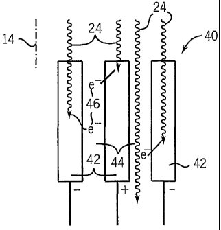
[0042] Referring now to Fig. 3, a detector 40 of the present invention
provides for a
series of longitudinally extending converter elements 42 aligned generally
with the local
radiation axis 14 of radiation propagation. The converter elements 42 may be,
for
example, planar vanes or may be rods or other shapes.
[0043] Converter elements 42 are separated from each other in a direction
transverse to
the radiation axis 14 to create interconverter volumes 44 such as may be
filled with an
ionizing medium such as a gas including, for example, xenon. The gas may be
compressed in a housing (not shown) so as to increase the odds of electron-gas
interaction in the interconverter volumes 44.
[0044] MeV x-rays 24 received by the detector 40 strike the converter elements
42 to
produce high-energetic electrons 46 which proceed into the interconverter
volumes 44.
The electrons ionize the gas in the interconverter volumes 44. Some MeV x-rays
24'
will pass completely through interconverter volumes 44 without contacting the
converter
6
CA 02450229 2003-12-09
WO 02/103392 PCT/US02/19154
elements 42 and may produce some ionization. However, in the invention, this
ionization will be less than the ionization caused by high-energetic electrons
46 exiting
the converter.
[0045] Adjacent converter elements 42 may be given voltages of opposite
polarity so as
to provide a biasing field collecting the ionization charges whose flow may be
measured
using current detector circuitry well known in the art ionization detectors.
[0046] In this embodiment, the material of the converter element 42 is
preferably a
conductive metal so as to support the current flows of the ionization,
however, the
function of collecting charge may be separated from the function of converting
x-rays to
electrons and non-metallic converter elements having a conductive coating are
also
possible. Similarly, in tlus embodiment, the converter elements 42 are
preferably
composed of a high atomic number and/or high-density material so as to reduce
their
height and so as to provide efficient reduction of scattered x-rays like the
laminae 12
described with respect to Fig. 1. Nevertheless, it will be recognized that a
variety of
different materials may be used depending on manufacturing conveuence, the
energy of
the radiation, and the desire for compactness.
[0047] Referring now to Fig. 4, a detector array 50 may be created by
arranging a
number of converter elements 42 along an arc of constant radius about a focal
spot 52. A
radiation source is placed at the focal spot 52 to as to create a fan beam of
radiation
whose local radiation axes 14 are lines of radius from the focal spot 52 to
the detector
array 50. The converter elements 42 extending generally longitudinally with
respect to
the local radiation axis 14 but are also slightly tipped with respect to the
local radiation
axis I4. Referring also to Fig. 5, this tipping of the converter elements 42
increases the
area over which the radiation beam, for example, MeV x-rays 24' will strike a
converter
element 42 and not pass unintercepted through an interconverter volume 44.
Preferably,
the tipping will be equal to the width of the converter element 42 in the
transverse
direction over the height of the converter element in the longitudinal
direction.
However, more or less tipping may also be used, including none as will be
described
below. When the converter elements 42 are tipped, the height and width of the
converter
elements 42 may be adjusted to ensure that a path length 56 of MeV x-rays 24'
through
the converter element 42 is sufficient to ensure probable absorption of the
MeV x-rays
24' .
[0048] The slopped sides of the converter elements 42 such as produced by the
tipping
as shown in Fig. 4 need not be monotonic but adjacent converter elements 42
may
7
CA 02450229 2003-12-09
WO 02/103392 PCT/US02/19154
alternatively have, for example, interdigitating projections so as to preserve
an
interconverter volume 44 but to expose no direct through path between
converter
elements 42.
[0049] Refernng to Fig. 6, the preferred dimensions of the converter elements
42 will
depend on the radiation energy, the material of the converter elements 42 and
the desired
resolution of the detector. Generally the centerline spacing SS of the
converter elements
42 will be determined by the spatial resolution desired in the resultant
detector. The
width S4 of the converter elements 42 will depend on their material and a
tradeoff
between the spacing SS between converter elements 42 which determines the
width S7 of
detector material and the width S4 of the converter elements 42 which
determine the
amount of conversion, both which relate to conversion efficiency. Potentially
the
tluckness of the converter element 42 may be quite small making use of
breakthroughs in
the production of so-called namo-wires of extremely small diameter.
[0050] Referring now to Fig. 7, a conventional CT ionization-type KeV detector
S8 such
as one manufactured by the General Electric Company for its KeV CT machines
may be
applied for use with MeV x-rays using the present invention's mechanism of
generating
electrons using the laminae of the detector as converter elements 42. Absent
recognition
of the conversion properties of the laminae, use of such a detector for MeV
radiation
would be comter intuitive because of the expected low interaction of MeV
radiation with
the inter-laminae gas. This particular detector S8 provides in effect an array
of S0, 738
converter elements 42 formed from the tungsten laminae,. Up to S00 -volt
potential may
be applied across adjacent converter elements 42 in an alternating
configuration. For a
fan beam detector, the height of the detector may be 3.56 cm and the detector
may be 44
cm long to measure a six MeV beam.
[0051] Improved sensitivity may be provided by defocusing the detector S8. As
shown
in Fig. 7, an actual focal point 60 is defined by the orientation of the
laminae 12 such as
divided the ionization chamber into detector volumes 16. Focal point 60 maybe
displaced typically inward by a predetermined amount 6I from the focal spot S2
of the
MeV x-rays thus causing the x-rays from focal spot S2 to strike the laminae 12
at an
angle increasing the absorption of radiation and their liberation of
electrons. For
example, the detector S8 may have a focal point of 103.6 cm and be placed 141
cm away
from focal spot S2.
[0052] Referring to Fig. 8, the centermost lamina 12 in region 64, which
despite this
displacement are essentially aligned with radiation from the focal spot 52,
exhibit a
8
CA 02450229 2003-12-09
WO 02/103392 PCT/US02/19154
decreased sensitivity in comparison with those off center lamina in regions 66
which are
receiving radiation directed against their sides as well as their ends. Edge
most laminae
12 in regions 68 exhibit decreased sensitivity because of shadowing caused by
adjacent
laminae 12.
[0053] Referring now to Fig. 9, an areal detector 70 may be constructed along
the
principals described above, by using a set of longitudinally aligned tubes 72
having
coaxial wires 74. Here the interconverter volumes 44 are those spaces between
the walls
of the tubes 72 and the wires 74. Inter-tube regions 75 do not serve for
detection in this
embodiment but are relatively minor in area.
[0054] In this embodiment, the coaxial wires 74 may be given a positive charge
to
collect negative charge Garners formed by ionization of gas held in the
interconverter
volumes 44 between the wires 74 and the walls of the tubes 72 or vice versa.
Here both
tubes 72 and wires 74 provide for conversion properties projecting liberated
electrons for
detection. It will be understood that the tubes 72 may be packed to define an
arbitrary
area and that each tube 72 and coaxial wire 74 defines a detector element.
[0055] Referring to Fig. 10, in an alternative embodiment, the space between
the wire 74
and tube 72 (converter materials) may be filled with a semi-conductor material
such as
amorphous selenium 76 (detector material) so as to produce hole-electron pairs
which
may be collected by the electrodes formed by the wire 74 and tube 72.
[0056] Referring now to Fig. 11, in yet a further embodiment, the wire 74 may
be
dispensed with and the tube 72 filled with a scintillator material 80
receiving the
liberated electrons 46 and emitting a photon 82 for detection by a solid-state
photo
detector 84. The use of the structure of tubes 72 limits the necessity that
the scintillator
material 80 have significant conversion properties (of converting radiation to
photons) or
be highly transparent (as its height may be limited by proper choice of the
converter
materials of the tube 72). This allows lower cost scintillating material to be
used.
It will be understood from the above description, that the above described
invention
employing a generating and liberating electron mechanism may be used for I~eV
or
lower energy radiation including visible light. Generally, the dimensions of
the detector
structures are fully scalable with the energy of the incident radiation.
Higher energy of
the incident radiation translates to larger detector structures (converter
material and
detection material), and lower energy of the incident radiation translates to
smaller
detector structures. As used herein, converter materials are the materials
that covert
radiation photons to electrons and detector materials are materials that are
used in the
9
CA 02450229 2003-12-09
WO 02/103392 PCT/US02/19154
detection of the electrons (e.g. ionizable gasses or semiconductors). The
lower limit of
scalability is only determined by atomic dimensions. Thus, the converter
material can be
of a nanometer scale (nanostructure), e.g., having dimensions (for example the
width of
the converter elements) less than 100 nanometers.
[0057] The longitudinal converter mechanism also has potential application in
the field
of radiation sensitive films where converter structures, possibly in the form
of freely
dispersed filaments or aligned filament structures using electrostatic
techniques and the
like, may be embedded in the emulsion of the filin itself with liberated
electrons
interacting with the silver compounds of the emulsion to produce a higher
sensitivity in
the film than that wluch would normally be provided by the film alone.
[0058] It is specifically intended that the present invention not be limited
to the
embodiments and illustrations contained herein, but that modified forms of
those
embodiments including portions of the embodiments and combinations of elements
of
different embodiments also be included as come within the scope of the
following
claims. For example, the use of semiconductor detectors or scintillation
detectors could
be used with the embodiment of Fig. 4.