Note: Descriptions are shown in the official language in which they were submitted.
CA 02450378 2008-01-17
, ..
SYSTEM AND METHOD FOR POST FILTERING PEAK POWER REDUCTION IN
COMMUNICATIONS SYSTEMS
BACKGROUND OF THE INVENTION
1. Field of the invention
The present invention relates to communications systems that transmit
signals that may be composed of one or more combined transmit carriers. Each
of
these carriers may include one or more communication channels. More
particularly, the present invention relates to wireless communications systems
and
signal processing apparatus employed in wireless communications systems. The
term 'wireless communications systems' includes cellular communication
systems,
personal communication systems (PCS), wireless local loop systems, and all
other
like systems.
2. Background of the Prior Art and Related Information
Wireless communications systems employing transmission between base
stations and remote users are a key component of the modern communications
infrastructure. These wireless systems are being placed under increasing
performance demands that are taxing the capability of available equipment,
especially wireless base station equipment. These increasing performance
demands are due to both the increasing numbers of users within a given
wireless
region, as well as the bandwidth requirements allocated to wireless system
service
providers. The increasing number of wireless users is of course readily
apparent
and this trend is unlikely to slow due to the convenience of wireless
services. The
second consideration is largely due to the increased types of functionality
provided
by wireless systems, such as wireless Internet access and other forms of
wireless
data transfer over such systems. These considerations have resulted in a need
CA 02450378 2003-12-10
WO 03/005594 PCT/US02/20422
for more communication channels per carrier and more carriers operating from
each transmitting location of a wireless service network.
One method of transmitting multiple communication channels on a single
carrier is to use a code multiplexed signal generator as shown in Figure 1.
Data
channels from different users enter the code multiplexed signal generator I to
produce a complex signal output represented by in-phase and quadrature-phase
components V, and V2 respectively. This complex signal output is then band
limited by filtering 2, converted to a baseband analog signal by Digital-to-
Analog
(D/A) conversion 3, modulated to an RF frequency 4, amplified 5 and
transmitted
by an antenna 6. This method is used by wireless systems providing CDMA
(Code Division Multiple Access) or WCDMA (Wideband Code Division Multiple
Access) services.
Other methods exist for combining several communication channels onto a
single carrier. For example the code multiplexed signal generator 1 in Figure
1
could be replaced with a time multiplexed signal generator. As before multiple
input data signals would be combined to produce a complex signal output
represented by in-phase and quadrature-phase components V, and V2
respectively. NADC (North American Digital Cellular) and GSM (Global System
for
Mobile Communications) wireless service providers use time multiplexed signal
generators.
For single carrier generation, the signal generator 1 of Figure 1 and the
filter
2 create signal peaks which determine the peak-to-average ratio of the signal
which must be D/A converted 3, modulated 4, and amplified 5. High peak-to-
average ratios require increased cost in these components. D/A converters with
large bit counts must be used to both create the large peaks and maintain
adequate signal resolution to overcome noise generated in the D/A conversion
process. High peak-to-average ratios require the use of very linear RF up
converting modulator and power amplifier components to prevent signal
distortion
from increasing carrier bandwidth through distortion and intermodulation.
Signal
2
CA 02450378 2003-12-10
WO 03/005594 PCT/US02/20422
bandwidth is government regulated. Increased carrier bandwidth may cause
operation outside government allocated operating bands in violation of the
law.
Figure 2 shows a prior art multiple carrier communication system. Figure 2
shows signal generation of M complex signals Vm,l and Vm,2. Each complex
signal would then be filtered 2, offset in frequency 7, and combined 8 to
generate
a single complex signal. This combined complex signal would then be processed
in a manner identical to the single carrier signal after filtering 2 in Figure
1.
When generating a multiple carrier signal as shown in Figure 2, the output
signal peak-to-average ratio is determined by the signal generators 1, the
filters 2,
and the interaction of each carrier in combining 8. This multiple carrier
signal must
then be D/A converted 3, modulated 4, and amplified 5. As with the single
carrier,
high peak-to-average ratios increase the cost of the D/A converter 3, RF up
converting modulator 4, and amplifier 5 components.
In a previous approach, placing a signal-peak suppression block prior to
filtering 2 has been employed in an attempt to reduce the peak-to-average
ratio in
single carrier communication systems. This prior art approach is shown in
Figure
3. The signal-peak suppression block 9 operates by adjusting the input complex
signal prior to filtering. By making signal adjustments prior to filtering,
the resultant
adjustments do not affect signal bandwidth guaranteeing operation within
government allocated limits. The subsequent filtering introduces new peaks,
however, and the effectiveness of the prior signal-peak suppression block is
greatly reduced.
As mentioned previously, the peak power of a multiple carrier
communication system, as shown in Figure 2, is dependent on the signal
generators 1, filters 2, and interaction of each carrier in combining 8. The
approach shown in Figure 3 if inserted prior to filtering 2 in Figure 2 would
be
incapable of correcting for the interaction of each carrier in combining. This
limitation would eliminate most, if not all, benefits of such an application
of prior
art.
3
CA 02450378 2003-12-10
WO 03/005594 PCT/US02/20422
In single carrier communication systems it is often difficult to place a peak
reduction block before filtering 2 and obtain effective peak reduction.
Applying
previous art in a multiple carrier communication system would prove
ineffective.
Therefore, a problem exists in prior approaches to reducing high signal peaks
in
communications systems.
SUMMARY
In a first aspect the present invention provides a communication system
comprising a communication signal source providing a band limited
communication signal; for example, the communication system may be a multi-
carrier communication system or a spread spectrum communication system. A
peak reduction unit is coupled to receive the band limited communication
signal
and provide a band limited peak reduced output signal. The peak reduction unit
comprises a circuit for providing a peak reduction correction waveform
corresponding to the difference between the communication signal and the
communication signal hard limited to a limit value and a correction filter for
filtering
the peak reduction correction waveform and providing a band limited peak
reduction correction signal corresponding to the band limits of the
communication
signal. A combiner receives the band limited communication signal and the band
limited peak reduction correction signal and combines them to provide a band
limited peak reduced output signal. The peak reduction unit also preferably
comprises a delay for delaying the band limited communication signal and
providing the delayed signal to the combiner. The communication system may
further comprise a digital-to-analog conversion stage for converting the peak
reduced output signal to an analog signal, a power amplifier receiving and
amplifying the analog signal, and an antenna coupled to the output of the
power
amplifier.
In a further aspect, the present invention provides a peak reduction unit
adapted for use in a communication system. The peak reduction unit comprises a
first signal path and a second parallel signal path. The first signal path
receives a
band limited input signal and includes a delay circuit for delaying the input
signal.
4
CA 02450378 2003-12-10
WO 03/005594 PCT/US02/20422
The second parallel signal path also receives the band limited input signal
and
includes a peak reduction calculation unit for calculating a peak reduction
correction and a filter providing a filtering operation on the peak reduction
correction. The peak reduction unit further comprises a combiner combining the
filtered peak reduction correction and delayed input signal and providing peak
adjusted output signals.
In a preferred embodiment of the peak reduction unit, the second signal path
further comprises a signal magnitude detector, a comparator for comparing the
signal magnitude to a predetermined limit value and a switch coupled to the
output
of the comparator and the peak reduction calculation unit for selecting the
peak
reduction correction if the signal magnitude exceeds the predetermined limit
value.
The second signal path may also include a gain circuit for adjusting the
magnitude
of the correction by a gain value. The gain circuit may comprise a multiplier
receiving the peak reduction correction signal and multiplying it by the gain
value.
The gain value should be less than 1 when the peak impulse response of the
correction filter is normalized to 1. In a more general case the gain value
should
be greater than zero but less than a level that would cause the peak to
average
ratio to begin increasing. The input signal may comprise digital samples
represented by complex vectors and the peak reduction calculation unit may
comprise an algorithm processor which performs a complex vector calculation on
the input samples to determine a complex correction vector which when added to
the input sample results in a signal magnitude at or within a predetermined
limit
value. The combiner preferably comprises an addition circuit. The filter
provides a
filtering operation limiting the correction signal to a frequency band
corresponding
to the spectral band of the band limited input signal and may comprise a
finite
impulse response filter.
In a further aspect, the present invention provides a method for signal peak
reduction in a communication system where the communication signal is
processed to limit the signal bandwidth to a predetermined spectral band. The
method comprises receiving as an input a band limited communication signal and
determining a peak reduction correction signal based on the amount the band
5
CA 02450378 2003-12-10
WO 03/005594 PCT/US02/20422
limited communication signal exceeds a threshold peak power value. The method
further comprises filtering the peak correction signal to limit the bandwidth
of the
peak correction signal and combining the filtered peak correction signal and
input
filtered communication signal to provide a peak reduced output communication
signal. Preferably the input communication signal is delayed prior to
combining
with the filtered peak correction signal.
Preferably the method for signal peak reduction further comprises adjusting
the peak correction signal by a gain value before the combining. Also, the
determining, gain adjusting, filtering and combining may be repeated employing
a
different gain value. The determining preferably comprises performing a peak
reduction algorithm on the input communication signal. The method for signal
peak
reduction may further comprise detecting the magnitude of the input
communication signal and comparing the magnitude to a peak limit value and
selectively outputting the peak reduction correction signal to be filtered and
combined only when the magnitude of the input communication signal exceeds
the magnitude of the peak limit value. Preferably the filtering operation
limits the
peak reduction correction signal to a frequency band corresponding to the
spectral
band of the communication signal.
The method for signal peak reduction may be employed in a multi-carrier
communication system wherein the communication signal is a multi-carrier
signal
provided by combining a plurality of separate carrier signal sources, each
having a
stream of carrier symbols corresponding to one or more data channels.
Alternatively, the method for signal peak reduction may be employed in a
spread
spectrum communication system wherein the communication signal is a spread
spectrum signal provided by combining a plurality of separate streams of
communication symbols corresponding to a plurality of data channels.
Accordingly, it will be appreciated that the present invention provides a
system and method for signal peak reduction, adapted for use in a
communication
system incorporating a source of a band limited communication signal, which
provides signal peak reduction of the communication signal without violating
the
6
CA 02450378 2003-12-10
WO 03/005594 PCT/US02/20422
band limits of the communication signal or the modulation scheme of the
communication signal. Further features and aspects of the present invention
will
be appreciated by reviewing the following detailed description of the
invention.
BRIEF DESCRIPTION OF THE DRAWINGS
Figure 1 is a block schematic drawing of a prior art single carrier
communications system.
Figure 2 is a block schematic drawing of a prior art multiple carrier
communications system.
Figure 3 is a block schematic drawing of a prior art single carrier
communications system with peak reduction performed prior to filtering.
Figure 4 is a block schematic drawing of the present invention showing
signal-peak suppression just prior to D/A conversion in a single carrier
communication system.
Figure 5 is a block schematic drawing of the present invention showing
signal-peak suppression just prior to D/A conversion in a multiple carrier
communication system.
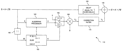
Figure 6 is a detailed block schematic drawing of the signal-peak
suppression unit shown in Figure 4 and Figure 5.
Figure 7 shows a complex signal vector diagram detailing the calculation of
the correction signal used to suppress the output signal peak power.
Figure 8 shows the impulse response function of the correction filter used to
limit the bandwidth of the correction signal calculated in Figure 7.
7
CA 02450378 2003-12-10
WO 03/005594 PCT/US02/20422
Figure 9 shows the effect filtering has on an example correction signal and
illustrates the advantages of gain weighting the correction signal.
Figure 10 shows a graphical approach to determining the gain weighting
constant used.
DETAILED DESCRIPTION OF THE INVENTION
A preferred embodiment of a single carrier communications system
employing signal-peak suppression (or reduction) in accordance with the
present
invention is illustrated in Figure 4. A preferred embodiment of a multiple
carrier
communications system employing signal-peak suppression in accordance with
the present invention is illustrated in Figure 5.
Referring to Figure 4, a communication signal, which may comprise a
digitally sampled signal stream represented by an in-phase component signal
stream A and a quadrature-phase component signal stream B, is input to a
signal-
peak suppression unit 110. This digitally sampled signal stream may contain
one
or more communications channels as produced by the signal generator 10 and
filter 20. The signal-peak suppression unit outputs a peak-reduced signal
stream
represented by an in-phase component signal stream A' and a quadrature
component signal stream B'. This signal-peak suppression output signal is then
D/A converted at D/A converter 30, modulated onto a RF carrier at RF up
converting modulator 40, amplified by power amplifier 50, and transmitted with
an
antenna 60.
Referring to Figure 5, a preferred embodiment of a multiple carrier
communications system employing signal-peak suppression in accordance with
the present invention is illustrated. A communication signal, which may
comprise
a digitally sampled signal stream represented by an in-phase component signal
stream A and a quadrature-phase component signal stream B, is input to a
signal-
peak suppression unit 110. This digitally sampled signal stream may represent
one or more transmit carriers with each of these transmit carriers providing
one or
8
CA 02450378 2003-12-10
WO 03/005594 PCT/US02/20422
more communication channels as produced by the signal generators 10, filters
20,
frequency converters 70 and combiner 80. The signal-peak suppression unit
outputs a peak-reduced signal stream represented by an in-phase component
signal stream A' and a quadrature component signal stream B'. This peak-
reduced signal is then D/A converted at D/A converter 30, modulated onto a RF
carrier at RF up converting modulator 40, amplified by power amplifier 50, and
transmitted with an antenna 60.
In both the embodiment of Figure 4 and Figure 5, the communication signal
which is input to the peak suppression unit 110 is band limited to a band
corresponding to the spectral band allocated to the communication system,
typically by a government body such as the FCC (Federal Communication
Commission). This band limiting is typically provided by filters 20. These
filters
may be viewed as modulation filters since in addition to limiting the signal
band to
the allocated spectral mask the trajectory of the signal waveform is modified
in a
manner that must be consistent with the modulation scheme. As will be
discussed
in detail below the signal peak suppression unit 110 peak suppresses the
communication signal without violating the spectral band or the modulation
scheme.
Referring to Figure 6, a detailed embodiment of the signal-peak
suppression unit 110 of Figure 4 and Figure 5 is illustrated. The signal-peak
suppression unit processes the in-phase and quadrature-phase component
streams A and B as a single complex signal stream S. The signal-peak
suppression unit includes a first signal path with a delay 120 and a parallel
correction signal path. An algorithm processor 140 in the correction signal
path
calculates a correction vector C based on each sample of S and a signal
limiting
constant L. The magnitude of each sample of S is determined at 180 and input
to
a switch driver 190, which controls switch 150. Switch 150 selects either the
calculated correction vector C or the value zero depending on whether the
magnitude of the current sample of S exceeds the limiting constant L. The
output
of switch 150 represents the difference between the input signal stream S and
a
version of S hard limited to the amplitude L. The output of the switch is then
9
CA 02450378 2003-12-10
WO 03/005594 PCT/US02/20422
adjusted by a gain constant g at multiplier 160 to create the correction
signal
stream Vc. The correction signal stream Vc is then filtered with a correction
filter
170 to create the filtered correction signal stream VF. The filtered
correction signal
stream VF is then combined at combiner 130 with a time-delayed version of the
input complex signal stream S. The combined signal stream is the peak-adjusted
output signal stream S' that can be represented as in-phase component A' and
quadrature component B' signal streams.
It is important to notice that the output signal stream S' is created from a
delayed version of the input signal stream S and the filtered correction
signal
stream VF. The filtered correction signal VF acts as interference to the
transmission of data to the intended communication channel users. The gain g
adjusts the level of interference. If the gain g were set to zero the signal
stream S
would be transmitted without interference. Notice that the only change to the
input
signal stream S is the addition of VF. The input signal stream S is not
changed by
either time varying gain control or filtering. Both filtering and time varying
gai.n
control of the signal stream S.would cause signal changes. Such changes would
act to affect the modulation of the input signal stream S. In the present
invention
the modulation of the input signal stream S is unaffected by the addition of
the
filtered correction signal stream VF.
The correction signal stream Vc comprises a waveform and thus has an
associated bandwidth. The correction filter 170 is employed to limit the
bandwidth
of the correction waveform of the correction signal stream Vc. The bandwidth
and
frequency dependent gain of the correction filter should be set to meet the
government allocated bandwidth requirements of the desired communication
signal. In the single transmit carrier case, the correction filter can be set
to match
the filter characteristics of the filter 20 shown in Figure 4. In the multiple
carrier
case, the correction filter bandwidth should be set to cover all transmitted
carriers.
The correction filter will time delay the correction signal stream Vc
requiring a
matching time delay, provided by time delay circuit 120, to signal stream S
prior to
signal combination with VF. Time delay circuit 120 should also include any
CA 02450378 2003-12-10
WO 03/005594 PCT/US02/20422
additional delays associated with the correction signal path, e.g., such as
due to
algorithm processor 140. This signal combination produces S' in Figure 6.
The algorithm processor 140 uses Equation (1) below to calculate the
correction vector C for each sample of S. This equation was developed
geometrically from Figure 7. Figure 7 shows a time trajectory segment of the
complex input signal stream S and a vector representing a single sample of S.
At
the time instant of the sample shown, the complex input signal S exceeds the
limiting constant L by the complex vector C, The complex vector C is
calculated
using Equation (1).
C= LISI-S (1)
Referring to Figure 6, the correction vector C only contributes to correction
signal stream Vc when the magnitude of a complex input signal sample of S
exceeds the limiting constant L. If the output from the switch 150 were added
directly to the input complex signal stream S, the output peak power would be
clamped to the limiting constant L. Unfortunately, the bandwidth of the switch
output would exceed the government allocated bandwidth required for the output
signal. To limit the switch output bandwidth, the correction signal stream Vc
is
passed through the correction filter.
Each input sample to the correction filter will produce an input sample gain
adjusted reproduction of the correction filter impulse response function at
the filter
output. These reproductions are combined to produce the correction filter
output.
Figure 8 shows a typical impulse response function that may be produced by a
correction filter. This impulse response function is shown for example
purposes
only. The impulse response function used in an actual functioning system will
be
determined by system needs. It is instructive to examine the correction filter
output based on a few simple example Vc signal streams.
11
CA 02450378 2003-12-10
WO 03/005594 PCT/US02/20422
Consider a short duration peak signal stream S that produces a correction
signal Vc composed of two equal amplitude correction samples in time sequence.
These two correction samples would be preceded and followed by zero valued
samples based on the switch 150 selection. The correction filter input and
output
signals Vc and VF for this example are both shown in Figure 9. The two non-
zero
input samples of Vc are just over 0.6 in amplitude. The figure shows how the
impulse response function of the correction filter acts on VC; to create VF.
The
filtered correction signal amplitude F corresponds to the input signal
correction
amplitude C in Figure 9. To prevent over compensation, a gain adjustment g
must
be applied in the correction signal generation path prior to combining with
signal S
in Figure 6. For the example shown, Figure 9 calculates this gain g by simply
taking the ratio of C over F.
The gain calculation in the last paragraph was specific to the example Vc
sample stream described. If the correction filter input signal stream were
just one
correction sample proceeded and followed by zero valued samples, the filter
input
and output amplitudes would have been the same at the required correction
instant. In this second example, the gain g calculated would have been one.
The two examples used to evaluate the gain constant g provided different
gains for different correction signal input examples. Any real correction
signal Vc
will produce an infinite number of similar type examples. The gain constant g
used
must provide the best possible peak signal suppression for all possible
variations
in Vc. Typical variations in Vc can be determined by performing a trial using
a
representative fixed time length complex input signal S, and a fixed limiting
constant L. With a typical Vc signal produced, a series of test trials can be
performed with different gain g constants. From these trials curves of S' peak-
to-
average ratio versus gain g and VF signal power versus gain g can be plotted
to
determine the best performance producing gain g value.
12
CA 02450378 2003-12-10
WO 03/005594 PCT/US02/20422
Figure 10 shows an example set of these curves for a specific test case.
The exact particulars of the test case are not important. The curves are shown
as
an example on how to select the best performing gain g constant. One curve in
Figure 10 shows the power of VF measured relative to the power in S just prior
to
combining with S. The other curve shows the peak-to-average ratio of the
output
signal S'. VF signal power represents distortion in the output complex signal
S'.
VF signal power should be kept to a minimum to avoid degrading overall system
communication quality. Figure 10 shows that lower gains produce lower VF
signal
power but also lower reduction in S' peak-to-average ratio. The S' peak-to-
average ratio curve shows a knee in the peak-to-average reduction at g equal
to
0.4. Increasing gain g much beyond 0.4 could increase the output signal
distortion
caused by VF without significant additional suppression of peak power.
The gain g selection demonstrated above was shown for demonstration
purposes only. In an actual system the gain g would depend on the specific
input
signal S, the limiting constant L, and the correction filter design used. The
gain
value should be less than 1 when the peak impulse response of the correction
filter is normalized to 1. In a more general case the gain value should be
greater
than zero but less than a level that would cause the peak to average ratio to
begin
increasing.
Finally, further signal-peak suppression can be achieved by cascading in
series multiple signal-peak suppression units 110 shown in Figure 4 and Figure
5.
By cascading signal-peak suppression stages less signal distortion will be
present
in the eventual output signal than if a larger gain value were selected in a
single
stage process. The method shown in Figure 10 should be used to determine the
gain g constant for each stage. Since the input to each successive stage is
already peak reduced, the gain g constant should be optimized to a different
value
for each stage. When performing test trials on successive stages the input
signal
used should be the peak-reduced signal from the preceding stage where the gain
g has been previously optimized. If the limiting constant L is the same for
each
13
CA 02450378 2003-12-10
WO 03/005594 PCT/US02/20422
successive stage, the output signal peak will closely approach the limiting
constant
L within two or three successive stages.
The present invention thus provides a communications system employing a
signal-peak suppression unit that is inserted just prior to D/A conversion. By
doing
so, the complexity and cost of the D/A converters, RF up converting modulator,
and power amplifier will be reduced. Further features and advantages of the
present invention will be appreciated by those skilled in the art.
A number of different embodiments of the present invention have been
described in relation to the various figures. Nonetheless, it will be
appreciated by
those skilled in the art that a variety of additional embodiments are possible
within
the teachings of the present invention. For example, a variety of specific
circuits
implementing specific algorithms may be provided employing the teachings of
the
present invention and limitations of space prevent an exhaustive list of all
the
possible circuit implementations or an enumeration of all possible algorithms.
A
variety of other possible modifications and additional embodiments are also
clearly
possible and fall within the scope of the present invention. Accordingly, the
described specific embodiments and implementations should not be viewed as in
any sense limiting in nature and are merely illustrative of the present
invention.
14