Note: Descriptions are shown in the official language in which they were submitted.
CA 02450487 2003-12-11
Patent-Treuhand-Gesell scl~aft
fur aloktrisaho Gluhlampcn mbF3., Munich
Disahargo lamp with stabilized disaharg~ vessel plate
Tachrzical hold
The present invention relates to a discharge lamp that
is designed for dielectrically impeded discharges. Such
discharge lamps have an electrode set with the aid of
which dielectrical7.y impeded discharges are generated
in a discharge medium. The discharge medium is arranged
fox this purpose in a discharge space that is bounded
- by a discharge vessel of the discharge lamp. The
dielectrically impeded discharges are distinguished in
that there is provided between at leas~C a portion of
the electrode set and discharge medium a d~.electric
layer that forms the dielectric impediment from which
the name comes. In the case of lamps where it is
stipulated which electrodes operate as cathodes and
which as anodes, at least the anodes ors separated i.x~.
th~.s case by the dielectric layer of the so-called
dielectric barrier from the discharge medium_ Since
such discharge lamps have been known for some time,
various details of the general d~asign of discharge
lamps for dielectrically ~,mpeded discharges will not be
...=
considered furthar_
Prior Art
Discharge lamps far dielectricaliy impeded discharges
are of particular interest Since it hag become known
that relatively high efficiencies in the generation of
UV light and, with suitable phosphors, other light as
well, in particular visible light, can be generated
with the aid of a pulsed operating mode (US 5 604 410).
znter alia, interest attache' in thin case to lamps
which are also designated as flat .radiators and in the
case of which the discharge space is located between
CA 02450487 2003-12-11
two discharge vessel plates that are substantially
plane-parallel as a rule and of which at least one lo
at least partially transparent. Of course, it is
possible in this case to provide a phosphor layer that
is net directly transparent in the actual sense. Flat
radiators are of interest, for example, for
backlighting displays, monitors and the like.
Summary of the Invention
to
The present invention is based on the problem of
specifying a discharge lamp, designed for
dielectrically impeded discharges, of improved design.
The invention is directed, firstly, to a discharge lamp
having two discharge vessel plates between which a
discharge space is arranged, and an electrode set for
generating dielectrically impeded discharges in the
discharge space, which Electrode set is arranged on a
side, averted from the discharge space, of a first one
of the discharge vessel plates, the first discharge
vessel plate forming a dielectric barrier between the
electrode get and the discharge space, charaeteri2ed in
that the first discharge vessel plate is supported on
its side facing the electrode set by a stabilizing
plate.
the invention is further directed to a method for
producing such a discharge lamp, in which ther~ is
3o produced a discharge vessel having two discharge vessel
plates between which a discharge space is arrangQd, an
electrode Set for generating dielectrically impeded
discharges being arranged in the discharge space on a
side, averted from the discharge space, of a first one
of the discharge vessel plates, and the first discharge
vessel plate farming a dial~ctric barrier b~twsen the
electrode set and the discharge space, characterized in
that the first discharge vessel plate is supported on
its side facing the elecCrode Set by a stabilizing
CA 02450487 2003-12-11
- 3 --
plate.
Preferred embodiments are sp~cified in the dependent
claims.
The invention proceeds in this case from the fact that
it is known per se in the case of discharge lamps for
dielectrically impeded discharges to arrange the
electrodes or a portion of the electrodes outside the
discharge vessel and utilize a corresponding portion of
the discharge vessel wall as dielectric barrier. Since
the discharge vessel walls consist as a rule of glass,
they are well suited per se for this function. However,
the discharge vessel walls must also fulfil mechanical
tasKS and are therefore approximately a few mm thick,
depending on application. this holds the more so for
the flat radiators cons~.dered here, in the case of
which the plates must be designed to be relatively
solid because of geometrical reasons. In v=der to be
able to ignite and operate discharges in such discharge
lamps, however, it is necessary to apply comparatively
high voltages to the electrodes. This is attended,
however, by an increased outlay in the design of the
electric supply, that is to say the electronic ballast.
and a.n the safety design.
On the other hand, there are also difficulties
associated with the internal electrodes frequently used
to date, in particular as regards the production of the
dielectric coating, which is then. to be applied
separately. Specifically, this dielectric coating must
satisfy relatively high demands with regard to the
accuracy and the uniformity of the material thickness.
and with regard to the freedom from gaps. This is
certainly possible in principle, but is 8ssociated with
a technical outlay that causes high costs, and with an
unavoidable wastage.
Tn accordance with the invention, it is provided to use
CA 02450487 2003-12-11
- 4 -
one d~.scharge vessel wail, speciLicaily one of the two
discharge vessel plates, as dielectric barrier, but to
design this plate to be relatively thin in order to be
able to take account more effectively th~ ~lectrical
aspects anc~ the optimization oL the supply concerning
the thickness of the di~lectric barrier, or to m~asura
the thickness of the dielectric barrier in the
individual case exclusively according to such criteria_
Consequently, the discharge vessel plate (here also
designated as first discharge vessel plate) bearing the
electrodes is provided, as it were, in two-fold
fashion. Firstly, as the actual first discharge ves9el
plate that bears the electrodes and forms the
d~.electric barrier, arid secondly as an additional
stabilizing plate chat supports the rirsz discharge
vessel plate and stabilizes it mechanically. The
electrodes are therefore located in the case oL the
finished discharge lamp between the first discharge
2o vessel plate, on the one hand, and the stabilizing
plate, on the other hand (but not necQSSarily directly
therebetween). It is to be noted here, moreover, that
these designs need not apply to all the electrodes of
the discharge lamp, but can hold only ~or a portion of
the electrodes, preferably for the portion that is to
have a dielectric barrier. It is in this sense that the
term "electrode set° is also to be understood in the
claims.
The stabilizing plate can preferably be a continuous
plate, for example a glass plate, as it would serve
conventionally as discharge vase~1 plate. The term
"stabilizing plate° is to be understood, however, very
comprehensively with regard to the geometry and implies
merely that the stabilizing plate can act in a
stabilizing fashian in a flat sense. It need not
necessarily be continuous for th~.s purpos~, and can
thus also have cutouts. recesses and the like. There
can also be a grid design, for example. It is
CA 02450487 2003-12-11
- 5 -
advantageous, however, wh~n the stabilising plate forms
a touch guard with regard to the electrodes, which are
supplied with hXgh voltage.
In addition, of tours~, other materials than glass are
also conceivable, in particular with regard to ether
additional functions, as well. For example, the
stabilizing plate could serve simultaneously for
mounting, as cooling element or as electromagnetic
shield, and therefore be fabricated from plastics or
metals or other materials. In addition, the first
discharge vessel plate al9o need not necessarily be
constructed from glass. zt need only consist of a
dielectric that makes the necessary electric data
available, it being possible to adapt the plate
thickness as appropriate.
In principle, the stabilizing plat~ can already perform
its function whenever it supports and stabilises the
comparatively thin first discharge vessel plate only by
virtue of the fact that it is connected to the
remaining, that is to say second, discharge vessel
plate or to a frame connected thereto, that zs to say
is in any case a stabilizing part of the discharge
vessel. The stabilizing plate then takes over a part of
the mechanical stabilization of the overall discharge
vessel, which is taken over conventionally by the first
discharge vessel plate. In addition, the stabilizing
plate can in this case also prat~ct the fiirst discharge
vessel plate against damage from outside - even protect
against the outside pressure in th~ calm of a tight
extexnal Seal. Tn addition, the first discharge vessel
plate and the stabilizing plate can, of course, be
intercennected continuously in a planar fashion.
However, it is 8referred according to the invention
that the connection between two plates is performed
only at points, although these points are provided in
relatively large numbers and distributed over the
surfaces of the plates. In particular, in Cho case of
CA 02450487 2003-12-11
- 6 -
the arxar~,gement of the conn~cting points it is possible
to have regard to the pattern of the electrode set or
other boundary conditions. Moreover, the connecting
operation can be performed in this way more simply or
with less use of material. For example, bonding,
welding, soldering or fusing of the plates come into
consideration as connecting methods.
In the case of flat radiators, support elements are
frequently provided between the discharge vessel
plates, in particular in tha case of large flat
radiator formats. These support the di9charge 'pace
against a aossible external overpressure and sriorten
the bending lengths. The conn~eting points according to
the invention between the first discharge vessel plate
and the stabilizing plate should in this case
preferably be provided so tightly 'Chat at most only the
bending lengths defined by these support ~1~ments
result. However, the spacings between the connecting
points arc pr~forably yet more clearly smaller, fox
example at must half as large a5 the bending lengths
provided by the support el~ments.
It is possible in this case to provide a geometric
tuning between the arrangement of the support elements
and the arrangement of the connecting points. For
example, the connecting points or a few of them can be
provided substantially a~C the same points
(perpendicular to the plates in the corresponding
projection) as the support elements. Any p0551b1e
further conn~eting points can then subdivide the spaces
between the connecting points thus arranged. A tuning
between the arrangement of the support elements and the
arrangement of the connecting points is also suggested
because the aim is possibly to take account iri both
arrangements of the pattern of the electrode set and
the pattern of the discharges Lhat is associated
therewith.
CA 02450487 2003-12-11
7
The first discharge vessel plate can, moreover, bear a
phosphor layer on the side averted from the electrode
set, and/or also have a refJ.ector layer. Moreover, it
would also be possible for further electrodes to be
provided on this side which then likewise do not belong
to the electrode set arranged according to the
invention on the other side, in particular cathod~s.
Favorable numerical values for the thickness of the
rirsL discharge vessel plate can be between 0.1 and
0.8 mm, pr~t~rably between 0,2 and 0.7 mm and, with
particular preference, between 0.3 and 0.6 mm. The
stabilizing plate, in turn, can have a thickness of
between 0.4 mm and 3 mm, but is not restricted to this
range.
Particular preference is given to a structure of the
second discharge vessel plate in the case of which the
latter on the one hand is transparent. and on the other
hand has a frame projection of integrated design for
externally sealing the discharge space, and support
elements, designed in a fashion integrated ix~, the
second discharge vessel plate, for the support in
r~lation to the first discharg~ vassal plate. Reference
may be made for further details of this discharge lamp
structure to the previous applications WO 02/27761 and
w0 02/27759 of the same applicant.
A variant of the invention consists in connecting the
first discharge vessel plate to the second discharge
vessel plate, on the one hand, and to the stabilizing
plate, on the other hand. in one and the same method
step. Thi9 relates specifically to connection
techniques in the case of which the participating parts
must be heated. It is then possible for the entire
discharge vessel structure, at leant the three plates
mentioned, to be connected in a common heating step.
In this case, it is preferred to make use between the
CA 02450487 2003-12-11
two discharge vessel plates of spacers that firstly
maintain between these di3charge vessel plates a
spacimg that serves for filling the discharge vessel
with a discharge medium. After the filling, the
temperature can then be raised so far that the spacers
soften and the upper one of the two discharge vessel
plates sinks onto the lower one. Their own weight. or
else an additional weighting can ~erve for this
purpose.
The connection between the first discharge vESSel plate
and the Stabilizing plate can also be pezformed in a
similar way, and specifically as already ment~.oned,
preferably simultaneously with .the connection between
the two discharge vessel plates. The spacers could
consist of SF6 glass that has a softening point in a
suitable temperature range. If the solders cause slight
contamination or none, it is also possible to dispense
with spacers at this point, and so the first discharge
vessel plate and the stabilizing plate can be laid
directly on one another from the start. It is then
possible at the abovementioned temperature to fuse
Solder glass points, for exaxnp~.e, at the connecting
points, in order to connect the first discharge vessel
plate and the stabilizing plate.
8rist' daoariptioa o~ the dra~.rings
,An exemplary ambodim~nt is described below with thQ aid
of the f~.gure5. In this case, dischvsed individual
features can also be essential to the invention in
combinations other than those illustrated.
In detail,
Figure 1 shows a cross sectional illustration of a
detail of a discharge lamp according to the: invention
before it is finished, and
CA 02450487 2003-12-11
- 9 -
Figure 2 shows a plan view of the discharge lamp rrom
figure 1 for the purpose of illustrating the
arrangement of solder glass points in figure 1.
Preferred design of the invention
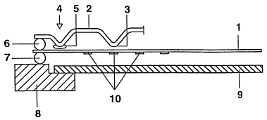
pigure 2 shows an illustration of a detail in a cross
section through a discharge lamp whose structural
details correspond, leaving aside the present
invention, to the illustrations in the earlier
applications WO 02/Z7761 and w0 02/27759 of the same
applicant. 1 designates a first discharge vassal plate,
the thickness or the glass plate being 0.4 mm. 2
designates a second di.scharg~ vessel plate,
specifically a transparent glass plate which has a
thickness of approximat~ly 1 mm ar~.d serves here as
' cover plate and for the exit of light. The second
discharge vessel plate 2 has a structure with inwardly
pointing supporting projections 3 which are of ~.ntcgral
design and run to a point onto the first d~.scharge
vessel plate 1, for which purpose reference may b~ made
to the already cited applications. In the outer, that
is to say in figure 1 left, region, the s~cond
discharc2e vessel plate 2 has a frame 4, likewise of
integral design, of which the underside, facing the
first discharge vessel plate 1, bears a solder glass
material 5.
Outside the frame 4, an outermost region of the second
discharge vessel plate 2 rests on a spacer 6 made from
SF6 glass, the arrangement actually lying in front of
and behind the plane of the drawing, as fellows from
figure 2_ The spacer 6 supports the second discharge
vessel plate 2 against the first discharge vessel plate
1 and. on the other hand leaves a passage to the (later)
discharge vessel interior between the discharge vessel
plates 1 and 2. In the state illustrated in figure 1,
the discharge vessel can therefore be rinsed and filled
from the plates 1 and 2.
CA 02450487 2003-12-11
- 10 -
The first discharge vessel plate 1 rests over a further
spacer 7, which corresponds otherwise to the spacer 6,
on a support 8 which sexves only to produce the
discharge vessel and does not belong to the discharge
vessel itself. Furthermore. a stabilizing plate 9,
specifJ.cally a glass plate with a thickness of
approximately 1 mm, rests on the support 8. In the
state illustrated in figure 1, the spacer ? ensures an
intermediate spacing between thA first discharge vess~al
plate 1 and the stabilizing plate 9.
Provided vn the side, lawer in accordance with
figure 1, of the first discharge vessel plate 1 are
electrodes (not illustrated in the figure) made from
silver (Rg)., which are therefore separated from the
(later) discharge space between the two plates 1 and 2
by the tlrst dlscharqe vessel plate 1. Distributed
furthermore on the sam~ low~r side of the first
discharge vessel plate 1 are solder qiass points lo,
concerning the arrangement of which reference is also
made to figure 2. xn figure 2, the solder glass points
10 are illustrated as points, and the supporting
proj ectivns 3 as crosses . fivwever, it is already to be
seen in figure 1 that one of the solder glass points
lies below the supporting projection 3 of the second
discharge vessel plate 2, and a further one of the
svldez- glass points 10 l~.ea in the region of the frame
5.
Figure 2 shows overall in a schematic plan view that
the solder glass points 10 form a squar~ grid, and the
supporting projections 3 form a face-centered square
grid, the grid spacing between the solder gJ.ass points
7.0 being half as large as that between the supporting
projections 3. In this case, the twe grids are aligned
on one another, and so solder glass points 10 are below
the supporting projections 3 in each case. The maximum
bending lengths between the supporting projections 3
are consequently halved by a solder glass point 10 in
CA 02450487 2003-12-11
_ 11 _
each case. In figure 2, the spacers 6, 7 are
illustrated in the outermost corners of the discharge
vessel plates 1 and Z, but they could also 1i~ at other
points. However, it suffices when they held the plates
1, 2 and 9 sufticiently~ apart from one another before
the final closure (after the filling) of the discharge
vessel.
According to the invention, after the filling of the
discharge space between the plates 1 and 2 and the
softening of the spacers 6 and 7, it is not only that
the solder glass layer 5 below the frame 4 fuses with
the first discharge vessel plate 1, but also the solder
glass points 10 on the underside of th~ first discharge
vessel plate 7, fuse with the Stabilizing plate 9. AS a
result, the vary thin first discharge vessel plate 1 is
connected in a planar fashion to the stabilizing plate
9, and is thus stabilized by the stabili2ing plate 9
both against external damage by impact or pressure, and
2o also with z~egard to bending loads of the discharge
vessel. In this exemplary embodiment, the interspace
between the first discharge vessel plate 1 and the
stabilizing plate 9 is not sealed in a vacuum-tight
fashion, and so atmospheric pressure is present during
operation between the two plates 1 and 9 and in the
event of a (typical) underpressure in the interior of
the da.scharge vessel a portion of the atmospheric
pressure rests On the first discharge vessel plate 1.
Since, however', th~ spacings between the solder glass
points 10 are sufficiently small, even the thin
discharge vessel plate 1 can withstand this external
overpressure.
A reflector layer i9 firstly arranged on the top side
of the first discharge vessel, plate 1, and a phosphor
layer is arranged above it. The dielectrically impeded
discharges generated by electrodes between the plates 1
and 2 produce VW radiation, which excites the phosphor
layer to emit visible light. The reflector layer lying
CA 02450487 2003-12-11
-- 12 -
below the phosphor J.ayer ensures optimization of the
utilization of the visible radiation for emission
upwards through the second discharge vessel plate 2.
The thickness of th~ first discharg~ v~ssol plate 1,
which amounts to 0.4 mm, offers a favorable layer
thickness for the di~lectric barrier on the electrodes
and requires no unnecessary outlay in the electrical
supply of the discharge lamp_ Thr~ stabilizing plate, in
turn, ensures touch protection, which corresponds to a
conventional variant with interior electrodes.