Note: Descriptions are shown in the official language in which they were submitted.
CA 02451003 2003-12-16
DESCRIPTION
INTEGRATED CIRCUIT DEVICE
Technical Field
s The present invention relates to an integrated circuit
device in which data flows can be reconfigured.
Related Art
When data and/or instructions (hereinafter referred to as "data"
Io where there is no particular need to distinguish between "instructions"
and "data', which are stored in a memory, such as a RAM, a ROM, or a
magnetic disc, are processed by a CPU or the like, a high speed memory
called a "cache" or "cache memory" that has a comparatively small
capacity is used and the access speed for the data is improved by
is utilizing the temporal locality and/or spatially locality of the data.
Accordingly, in an integrated circuit device such as a VLSI, a system LSI,
or a system ASIC where a processor or a processor core is incorporated,
a cache system comprising a cache memory and an MMU (Memory
Management Unit) for controlling the cache memory is also incorporated.
2o When a cache memory is used, an MMU and a TLB (Translation
Look-Aside Buffer) are used, so that when the data corresponding to a
virtual or logical address outputted from the CPU core is present in the
cache memory, data is inputted and outputted between the cache
memory and the CPU core. When the data is not present in the cache
2s memory, the virtual address is converted into a physical address by the
MMU and the TLB and an input/output is generated for an external
memory, and the data in the cache memory is also updated. In this way,
due to the cache control mechanism that comprises the MMU and the like,
i
CA 02451003 2003-12-16
the cache memory is constructed as a device that appears to be
transparent to the software that is executed by the CPU core.
Accordingly, software can be developed so as to operate based on virtual
addresses that do not depend on hardware, which makes it possible to
s reduce the time taken and cost incurred by software development and
design. Also, the same software can be run on different hardware,
which means that software resources can be used effectively.
When the data at the virtual address outputted from the CPU core
is not present in the cache memory, which is to say, when a "hit" does
to not occur for the cache memory, an input/output process occurs for an
external memory. When the hit rate of the cache memory is low, the
cache memory becomes merely an overhead that detrimentally affects
the execution time of programs. In order to improve the hit rate,
studies are being performed into techniques such as separating the cache
Is into an instruction cache and a data cache, constructing the cache with a
hierarchical structure, or prefetching data mechanically and/or using
software.
However, when applying the cache that is separated into an
instruction cache and a data cache, if instructions and data are
2o simultaneously present in one block, it becomes difficult to handle the
instructions and the data. For example, rewriting instructions may cause
obstruct to software processing. Also, in software where instructions
and data are not accessed equally, there is no improvement in efficiency
by simply separating the cache. For example, when the accesses to
2s data are sporadic, the usage efficiency of the data cache is low, so that
there is the possibility of this becoming an overhead.
A hierarchical cache is effective when there are large differences in
access time and storage capacity between the cache and the external
2
CA 02451003 2003-12-16
memory. However, when the cache is constructed hierarchically, there
is an inevitable rise in the number of accesses to the memory, so that
there is always the possibility of overheads depending on conditions such
as the structure of the software and the input/output media for the data
s being processed.
Even when prefetching is performed, penalties due to branch
instructions or the like cannot be avoided. In some kinds of software,
for example an arithmetical calculation program, in which many accesses
are preformed to array elements and the element to be accessed can be
to predicted in advance, the number of the cache penalties can be reduced
using prefetch instructions, though CPU time is expended by the
execution of such prefetch instructions and this technique can be used
effectively for limited range of software.
In this way, the above techniques are each capable of raising the
is hit rate of a cache memory in cases where conditions, such as the
software executed by a CPU and the media on which data is stored,
match with the selected method using the cache memory. However,
since cache memory is hardware that is disposed in an intermediate
position between the CPU and the external memory, when there are
2o differences in the processing content of the software to be executed or in
the hardware environment that stores the data to be processed by this
software, this can cause problems such as the predicted cache efficiency
not being obtained and conversely in overheads being produced, which
increases the execution time of the processor. For a processor that is
2s dedicated to a certain application, it may be possible to provide an
optimal cache memory system. However, for a processor that is
designed to have a certain degree of general-purpose applicability, to
ensure that the cache memory is worthwhile, it is necessary to provide a
3
CA 02451003 2003-12-16
cache memory system that does not cause many overheads, even if the
effectiveness of the cache memory system itself is not especially high.
Accordingly, even if a cache memory system is provided, the
improvement in performance is not especially large.
s It is an object of the present invention to provide an integrated
circuit device including a memory that can be used as a cache with the
highest possible efficiency for the processing content of software
executed by a processor and the hardware environment. It is a further
object of the invention to provide an integrated circuit device including a
to control function that can use a memory as a cache with the highest
possible efficiency. It is yet another object of the invention to provide
an integrated circuit device that can execute a variety of software more
efficiently.
15 DISCLOSURE OF THE INVENTION
In recent years, processing units in which the configuration of a
data path or a data flow can be at least partially changed have been
introduced. An FPGA (Field Programmable Gate Array) is an integrated
circuit device in which logic elements or logic blocks of the same
2o construction whose logic can be changed are laid out in an array, with it
being possible to change the interconnects between these elements or
blocks so as to change the configuration or construction of data paths.
Research is also being performed into integrated circuit devices where it
is possible to change the configuration of data paths using medium-scale
2s basic functional units of the same construction that perform a variety of
processes according to instruction sets. The applicant of the present
invention has developed a processing unit including (i) a plurality of types
of special-purpose processing elements, each type of special-purpose
4
CA 02451003 2003-12-16
element having internal data paths suited to respectively different
special-purpose processing, and (ii} sets of wires for connecting these
special-purpose processing elements. In this invention, a circuit that
controls a cache memory is configured using a part of these kinds of
s processing unit where the data flows can be changed or reconfigured.
This is to say, an integrated circuit device according to the present
invention includes a first memory for inputting data into and/or
outputting data from a second memory and a processing unit in which at
least one data flow is formed and at least part of at least one data flow is
to changeable, the processing unit including a data processing section that
processes data that is inputted from and/or outputted to the first
memory, a first address outputting section that outputs a first address of
data that is inputted and/or outputted between the first memory and the
data processing section, and a second address outputting section that
Is outputs a second address of data that is inputted and/or outputted
between the first memory and the second memory. By constructing a
first address outputting section and a second address outputting section
using part of the processing unit where the data flows can be changed,
using the hardware configuration of the data processing section or the
2o software executed in the data processing section, it is possible to change
the data flow of the first address outputting section or the second
address outputting section and to control the outputs of these sections.
Accordingly, a cache system that is optimal for the processing executed
by an integrated circuit device can be configured in the integrated circuit
2s device. Alternatively, it is possible to configure a control circuit for a
cache memory in the integrated circuit device so that a cache system can
be optimally controlled for the processing executed by the integrated
circuit device.
CA 02451003 2003-12-16
With the integrated circuit device of the present invention, the first
memory that is used as the cache memory can be passively controlled by
a second address in a second memory. The second address includes not
only a physical address of data in the second memory but also a logical
s address or virtual address that can be converted into the physical
address. Through such control, it becomes possible to make the first
memory is transparent to the second memory and/or the data processing
section. In addition, according to data or a signal from the data
processing section and/or the first address outputting section, the second
to address outputting section can actively control input and outputs of data
independently of both the data processing section and the first address
outputting section. It is also possible to control input/output operations
between the first memory and second memory in parallel with the
operations of the data processing section and the first address outputting
Is section. Accordingly, it is possible to configure a cache system where
the accessed location of data used by the data processing section and
first address outputting section is determined by the second address
outputting section, so that it is possible to construct not simply a
conventional cache that is transparent for a CPU but a cache that controls
2a the processing in the processing unit.
This is to say, conventional cache architecture is constructed so as
to provide a uniform, transparent interface that can improve the average
execution speed for software that operates on a processing structure of a
standardized hardware construction, such as a CPU core or a DSP core.
2s On the other hand, in the integrated circuit device of the this invention,
a
data processing section that acts as a core is provided by using an
architecture such as an FPGA in which the construction of a data path
itself can be changed, and in accordance with this, the cache construction
6
CA 02451003 2003-12-16
can be dynamically changed to an optimal construction for the
configuration in the data processing section and the software executed
by the configuration of the data processing section. Accordingly, there is
no need for always uniformity or transparency, and an interface or
service that is completely different to a conventional cache can be
provided for a data processing section that is the core or execution unit.
In this way, with the integrated circuit device of the present
invention, the first memory can be used with the highest possible
efficiency as a cache in accordance with the hardware environment and
to the processing content of the software executed by the processing unit.
A cache system that can produce a higher hit rate can be constructed
when a variety of software is executed, so that it is possible to provide an
integrated circuit device where input/outputs for a cache memory do not
cause overheads when a variety of software is executed.
is As one example, when the address in the second memory of data
to be executed by the data processing section is known, it is possible to
prefetch data using the remaining amount of space in the first memory
by the second address outputting section independently. Accordingly,
data can be prefetched into the second memory that is used as a cache
2o by hardware or by software that controls the second address outputting
section without consuming processing time of the data processing section.
In this example, an address in a first memory, that includes not only a
physical address in the first memory but also a virtual address or logical
address that can be converted into the physical address in the first
2s memory, is outputted from the first address outputting section as the
first address, and an address in a second memory, that includes not only
a physical address in the first memory but also a virtual address or
logical address that can be converted into the physical address is
CA 02451003 2003-12-16
outputted from the second address outputting section as the second
address. In the data processing section, hardware or software is
configured so that processing advances using addresses in the first
memory that acts as a cache memory.
s In addition, it is preferable for the second address outputting
section to be capable of operating asynchronously with, which is to say
independently of, the data processing section and/or the first address
outputting section. By doing so, data can be prefetched by parallel
processing independently of the data processing section. To make it
to possible to process inputs and outputs for the second memory
independently and in parallel, it is preferable to provide the first memory
with a plurality of storing sections, such as a plurality of memory banks,
for which inputs and outputs can be performed asynchronously or
independently.
Is It is also possible to configure the second address output section so
as to output the second address based on data in the first memory, by
the second address outputting section alone or by a combination of the
second address outputting section and the data processing section. By
this configuration, data processing can be executed by indirect
2o addressing with no limitations whatsoever.
It is preferable for the first memory that operates as a cache to
include a first input memory that stores data to be inputted into the data
processing section and a first output memory that stores data that has
been outputted from the data processing section. By doing so, inputs
2s and outputs of data for the data flows formed in the data processing
section can be controlled independently. An address in the first memory
is outputted from the first address outputting section, but when there is
no space for storing the data corresponding to the first address or there
s
CA 02451003 2003-12-16
is no data corresponding to the first address in the first memory, a failure
may occur in the processing of a data flow formed in the data processing
section. For this reason, it is preferable to provide a first arbitrating unit
that manages inputs and/or outputs between the first memory and the
s data processing section.
The first arbitrating unit can be provided with a function that
outputs a stop signal to the data processing section when the conditions
for input into or output from the data processing section are not satisfied,
such as when there is no data corresponding to the first address or when
to there is no space for storing data corresponding to the first address.
The data processing section can also be provided with a function for
stopping the processing of at least one data path or data flow that is
configured in the data processing section according to the stop signal, so
that the data path or data flow can be turned on and off by the first
is arbitrating unit. It is possible to easily realize control that has a data
path or data flow that is formed in the data processing section operate
after first waiting until the data to be processed is prepared.
If the first memory includes a first input memory and a first output
memory, it is preferable to provide a first input arbitrating unit that
2o manages data transfers from the first input memory to the data
processing section and a first output arbitrating unit that manages data
transfers from the data processing section to the first output memory as
the first arbitrating unit. It is possible to control data flows formed in
the data processing section independently from both the input side and
2s the output side.
When the first memory includes a plurality of storage sections that
are capable of independent inputs and outputs, the first arbitrating unit
can be provided with a function that manages the plurality of storage
9
CA 02451003 2003-12-16
sections independently. In this case, each of the plurality of data flows
formed in the data processing section can be controlled independently by
the first arbitrating unit according to the state of the corresponding
storing section. On the other hand, the first arbitrating unit can be
s provided with a function that manages a plurality of storing sections
relationally or with the storing sections being associated with one another.
By doing so, it is easy to realize control that has data flows formed in the
data processing section give priority to processing data that is inputted
into a predetermined storing section from an external memory and has
to outputs from data flows outputted with priority to the external memory
via a predetermined storing section.
In addition, when a plurality of data flows can be configured in the
data processing section, it is preferable to provide a plurality of first
memories and to have a pair of first and second address outputting
Is sections configured in the processing unit corresponding to each first
memory. It becomes possible to construct a multilevel or hierarchical
cache by appropriately configure the data processing section and the first
address outputting section. Also, depending on the program executed
by the integrated circuit device, a plurality of first memories can be
2o divided and used as an instruction cache and a data cache, and when a
plurality of data processing sections are provided, the plurality of first
memories can be used for caching the data processed by these data
processing sections and the data cached by the respective first memories
can be appropriately controlled by the second address outputting section.
25 When a plurality of second address outputting sections are
provided, a second arbitrating unit that manages inputs and outputs
between the second memory and the plurality of first memories should
preferably be provided and the second address should preferably be
Io
CA 02451003 2003-12-16
supplied to the second arbitrating unit. When the second memory is an
external memory, the integrated circuit device of the present invention
can access the external memory in the same way as a conventional
integrated circuit device. Also, in an integrated circuit device where the
s second memory is formed on the same chip, it is possible to construct
the cache memory hierarchically by providing a third address outputting
means that outputs a third address of the data that is inputted and/or
outputted between a third memory and the second memory so as to
make it possible to input and/or output data between the second
to memory and the third memory. This is to say, if the third memory is an
external memory, the cache memory can be composed of the first and
second memories. This third address outputting means may be a
conventional cache control mechanism such as an MMU, though it is also
possible for the third address outputting means to have a similar
is construction to the second address outputting section. This is also the
case when control is performed for a fourth or higher level of memory
(which is not restricted to ROM and RAM and may include various types
of storage media such as disks).
A processing unit in which the data flow can be changed or
2o reconfigured may include a type of processing unit that includes a
plurality of logic elements of the same type whose functions can be
changed and a set of wires for connecting these logic elements, which is
an FPGA above, and another type of processing unit in which the data
path arrangement or data flows can be changed using medium-scale
2s basic functional units of the same construction. It is also possible to use
a further different type of processing unit that includes (i) a plurality of
types of special-purpose processing elements, each type of the special-
purpose processing element including internal data paths suited to
11
CA 02451003 2003-12-16
respectively different special-purpose processing and (ii) sets of wires for
connecting these special-purpose processing elements. With this type of
reconfigurable processing unit, it is possible to incorporate special-
purpose processing elements including internal data paths that are suited
s to outputting addresses, so that the processing efficiency for generating
addresses is increased and the processing speed can be further improved.
Also, since there is a reduction in the number of surplus circuit elements,
a reduction can be made in the number of elements that are selected to
change the data flow, the AC characteristics can be improved, and an
to increase is also made in the space efficiency.
Accordingly, by having a control unit, which indicates changes to at
least part of a data flow in the processing unit, execute a process that
instructs the processing unit to construct the data processing section,
first address outputting section, and second address outputting section
is mentioned above, a data flow can be flexibly and dynamically changed in
a short time. This makes it possible to provide a compact, economical
integrated circuit device that includes a flexible cache system.
To facilitate changes in the data flows in the processing unit, it
should preferably be possible to, in addition to change the connections
2o between the special-purpose processing elements, to include (i) means
that select parts of the internal data paths of the special-purpose
processing elements and (ii) configuration memories that store selections
of the internal data paths. The control unit can reconfigure data flows
by rewriting the content of the configuration memories or by indicating
2s changes to at least part of a data flow in the processing unit. If the
processing unit includes special-purpose processing elements, the control
unit can indicate changes in the data flow in the data processing section,
the first address outputting section, or the second address outputting
12
CA 02451003 2003-12-16
section asynchronously and independently. While data is being inputted
into or outputted from the first memory, the special-purpose processing
elements that compose the data processing section and/or first address
outputting section can be used to configure a data flow for another
s purpose. Conversely, while processing is being executed by the data
processing section, the special-purpose processing elements of the
second address outputting section can be used to control a different
memory or be used for a different purpose, so that the resources of the
processing unit can be flexibly and efficiently utilized.
to By incorporating a code memory for storing program code that has
the control unit perform the above processing, it becomes possible to
construct an integrated circuit device, such as a single-chip system t_SI.
Accordingly, it becomes possible to provide integrated circuit devices with
improved execution speed where a cache or cashes are used efficiently
is for a variety of types of software without causing overheads. It is also
possible to provide a processing unit whose data flows can be
reconfigured as a separate chip, as a processor core, or as a chip in
which the first memory used as the cache memory is also incorporated.
In this way, the present invention can be embodied in a variety of ways,
2o with processing devices that correspond to such embodiments also being
included within the scope of the present invention.
Brief Description of the Drawings
FIG. 1 is a block diagram showing an arrangement of an integrated
2s circuit device according to an embodiment of the present invention.
FIG. 2 shows an arrangement of an AAP that is a processing unit.
FIG. 3 shows an arrangement of the matrix unit.
FIG. 4 shows an example of a data path potion that is suited to
13
CA 02451003 2003-12-16
processing that outputs addresses.
FIG. 5 is a diagram showing the construction of the address
generator of the data path portion shown in FIG. 4.
FIG. 6 is a diagram showing the construction of the counter shown
s in FIG. 5.
FIG. 7 is a diagram showing an arrangement of a different address
generator to FIG. 5.
FIG. 8 is a diagram showing how a large-capacity RAM is controlled
as an external memory.
to FIG. 9 is a diagram showing how a large-capacity RAM and a
peripheral device are controlled as an external memory.
FIG. 10 is a diagram showing how a plurality of large-capacity
RAMS and peripheral devices are controlled as an external memory.
FIG. 11 is a diagram showing how a large-capacity RAM is
is controlled as an external memory by a different integrated circuit device
according to the present invention.
Best Mode for Carr~ring Out the Present Invention
The following describes the present invention with reference to the
2o attached drawings. FIG. 1 shows the outline configuration of a system
LSI 10 according to the present invention. This LSI 10 is a data
processing system that includes a processor unit 11, an AAP (Adoptive
Application Processor) portion or unit (hereinafter AAP) 20, an interrupt
control unit 12, a clock generating unit 13, an FPGA unit 14, and a bus
2~ control unit 15. The processor unit 11 (hereinafter "basic processor" or
"processor") that has a general-purpose construction and performs
general purpose processing, including error handling, based on
instruction sets that are provided by a program or the like. In the AAP
14
CA 02451003 2003-12-16
unit 20, data flows or virtual data flows that are suited to special-purpose
data processing are variably formed by a plurality of operation or logical
elements that are arranged in a matrix. The interrupt control unit 12
controls interrupt handling for interrupts from the AAP 20. The clock
generating unit 13 supplies an operation clock signal to the AAP 20. The
FPGA unit 14 further improves the flexibility of the operation circuits that
can be realized by the LSI 10. The bus control unit 15 controls inputs
and outputs of data to and from the periphery. The FPGA unit 14 is an
interface for an FPGA chip that is disposed in the periphery of the LSI 10
to and is referred to hereinafter as the "offchip FPGA" and the '~FPGA". In
the LSI 10 that is the integrated circuit device of the present invention,
the basic processor 11 and the AAP 20 are connected by a data bus 17
on which data can be exchanged between the basic processor 11 and the
AAP 20 and an instruction bus 18 for enabling the basic processor 11 to
control the configuration and operation of the AAP 20. Also, interrupt
signals are supplied from the AAP 20 to the interrupt control unit 12 via a
signal line 19, and when the processing of the AAP 20 has ended or an
error has occurred during such processing, the state of the AAP 20 is fed
back to the basic processor 11.
2o The AAP 20 and the FPGA 14 are connected by a data bus 21, so
that data is supplied from the AAP 20 to the FPGA 14, where processing
is performed, and the result is then returned to the AAP 20. Also, the
AAP 20 is connected to the bus control unit 15 by a load bus 22 and a
store bus 23, and so can exchange data with a data bus on the outside of
the LSI 10. Accordingly, the AAP 20 can receive an input of data from
an external DRAM 2 or another device and output a result produced by
processing this data in the AAP 20 back to the external device. The
basic processor 11 can also input and output data to and from an
CA 02451003 2003-12-16
external device via a data bus 11a and the bus control unit 15.
FIG. 2 shows an outline of the AAP unit 20. The AAP unit 20 of the
present embodiment comprises a matrix unit or portion 28 in which a
plurality of logical blocks, logical units, and/or logical elements
s (hereinafter "elements") that perform arithmetical and/or logical
operations are arranged in a matrix, an input buffer 26 that supplies data
to the matrix unit 28, and an output buffer 27 that stores data that has
been outputted from the matrix unit 28. The input buffer 26 and output
buffer 27 respectively comprise four small-capacity input memories
to (RAMS) 26a to 26d and four output memories (RAMS) 27a to 27d. The
AAP 20 further comprises an external access arbitrating unit (second
arbitrating unit) 25 that controls data input/output operations between
(i) the bus control unit 15 and (ii) the input buffer 26 and output buffer
27 that comprise a plurality of memories.
is The input RAMs 26a to 26d and output RAMs 27a to 27d of the
present embodiment each functions as lKbyte dual-port RAMs, and each
can be used as dual-bank RAMs 81 and 82 that are 64k bits wide and
512 bytes deep. Accordingly, by using different banks for inputs and
outputs for the memory, it is possible to process input and output
2o operations independently. An arbitrating unit 85 (first arbitrating unit)
that manages inputs into and outputs from the RAMS 81 and 82 is also
provided and it is possible to check whether each bank is full or empty by
counting the number of inputs and outputs.
In order to control the inputting and outputting of data into the
2s input RAMs 26a to 26d and out of the output RAMS 27a to 27d, a plurality
of types of control signals are exchanged between (i) the matrix unit 28
and (ii) the RAMS and the arbitrating unit 85. First, 16-bit input readout
address data ("ira" or the "first address") 61 for controlling the data that
16
CA 02451003 2003-12-16
is read out by the matrix unit 28 from the input RAMS 26a to 26d is
outputted to each of the input RAMS 26a to 26d. The input readout
address 61 is a logical or physical address in the input RAMs 26a to 26d.
Also, an input readout address stop signal ("ira_stop") 62 for controlling
s the supplying of the address data 61 depending on the full and/or empty
states is outputted from the arbitrating unit 85 of each of the input RAMs
26a to 26d to the matrix unit 28. The input readout address stop signal
62 is also outputted from the arbitrating unit 85 when the input
conditions for the matrix unit 28 are not ready, such as when there is no
io data corresponding to the address data 61 supplied from the matrix unit
28.
In the matrix unit 28, a data flow or data flows that are formed in
the matrix unit 28 are turned on and off by the stop signals 62.
Accordingly, in the execution process that is performed after the data
is flows have been configured in the matrix unit 28, the execution of the
processing defined by the data flows can be respectively controlled by
the arbitrating units 85 of the input RAMs 26a to 26d. If the data that
corresponds to the input readout address data 61 is not present in the
input RAM 26, the processing of the data flow is placed into a wait state.
2o Conversely, if the data that corresponds to the input readout address
data 61 is present in the input RAM 26, 32-bit input readout data ("ird")
63 is supplied to the matrix unit 28, is processed by the configured data
flow, and is outputted to one of the output RAMs 27. Also, a stop signal
("ird stop") 64 that controls the input readout data 63 is outputted from
2s the matrix unit 28 to each of the input RAMS 26a to 26d so that the
reading out of data is stopped when the operation of the data flow in the
matrix unit 28 has stopped due to a cause on the output side, for
example.
m
CA 02451003 2003-12-16
The arbitrating unit 85 of each of the input RAMs 26a to 26d
fundamentally controls each of the input RAMS 26a to 26d independently.
Accordingly, the exchanging of data between the matrix unit 28 and the
input RAMs 26a to 26d is controlled and executed separately for each of
s the input RAMS 26a to 26d, so that data flows that are formed in the
matrix unit 28 corresponding to the input RAMs 26a to 26d are controlled
independently. This is also the case for the output RAMS 27a to 27d that
are described below. On the other hand, the arbitrating units 85 of the
input RAMs 26a to 26d can connect by wiring between the input RAMs
l0 26a to 26d or by wiring via the matrix unit 28, so that a plurality of
input
RAMS 26a to 26d can be managed relationally or associated with one
another. By managing input RAMS 26a to 26d relationally, it becomes
possible to assign a plurality of input RAMS to a data flow configured in
the matrix unit 28. By attaching an order of priority to the plurality of
Is input RAMs 26a to 26d using the arbitrating units 85, it is also possible
to
perform control that supplies data flows with data from RAMs with high
priority.
Also, 32-bit input write address data ("iwa" or the "second
address") 65, which controls the data to be read out from an external
2o memory 2 via the bus control unit 15 and written in each of the input
RAMs 26a to 26d, and a 4-bit control signal ("iwd_type") 66, which can
indicate the data type, etc., of the input data, are outputted from the
matrix unit 28 in the unit of each of the input RAMs 26a to 26d. The
input write address data 65 and the control signals 66 that correspond to
2s the respective input RAMs 26a to 26d are ail outputted to the external
access arbitrating unit 25. The input write address data 65 is a physical
address in the RAM 2, which is an external memory, or a logical or virtual
address that corresponds to the physical address in the RAM 2. In
Is
CA 02451003 2003-12-16
response to these addresses, stop signals ("iwa stop") 67, each of that
controls the output of the address data 65, are supplied from the
external access arbitrating unit 25 to the matrix unit 28.
Furthermore, 64-bit input write data ("iwd") 68 that corresponds to
s the input write address data 65 supplied to the external access
arbitrating unit 25 is respectively supplied from the arbitrating unit 25 to
each of the input RAMs 26a to 26d, and a stop signal ("iwd stop") 69
that controls the input write data 6~8 is supplied from each of the input
RAMs 26a to 26d to the external access arbitrating unit 25.
to In order to control outputs from the matrix unit 28, 16-bit output
write address data ("owa" or the "first address") 71 for controlling data
that is read out from the matrix unit 28 and written in each of the output
RAMs 27a to 27d is outputted to each of the output RAMs 27a to 27d.
This output write address data 71 is a logical or physical address in each
15 of the output RAMs 27a to 27d. An output write address stop signal
("owa stop") 72, which controls the supplying of the address data 71
based on full and/or empty states, is outputted from the arbitrating unit
85 of each of the output RAMS 27a to 27d to the matrix unit 28. This is
to say, when the conditions for the reception of an output from the
2o matrix unit 28 are not satisfied, the output write address stop signal 72
is
outputted from the arbitrating unit 85. In the matrix unit 28, the data
flows that are configured in the matrix unit 28 are turned on and off by
the stop signals 72, thereby controlling the execution of the processing
defined by the data flows. If there is space in the output RAM 27, 32-bit
2s output write data ("owd") 73 is outputted from the matrix unit 28
together with the output write address data 71. A stop signal
("owd stop") 74 that controls the output write data 73 is supplied from
the arbitrating unit 85 of each of the output RAMS 27a to 27d to the
19
CA 02451003 2003-12-16
matrix unit 28.
Also, 32-bit output readout address data ("ora" or the "second
address") 75 for controlling data to be read out from each of the input
RAMs 26a to 26d via the bus control unit 15 and written into the external
s memory 2 and a 4-bit control signal ("ord type") 76 that can indicate the
data type, etc., of this data are outputted from the matrix unit 28 in the
unit of the output RAMs 27a to 27d. The output read address data 75
and the control signals 76 are all outputted to the external access
arbitrating unit 25. The output read address data 75 is a physical
to address in the DRAM 2, which is an external memory, or a logical or
virtual address that corresponds to the physical address in the DRAM 2.
In response to this, a stop signal ("ora_stop") 77 that controls the
outputting of the address data 75 is supplied to the matrix unit 28 from
the external access arbitrating unit 25.
Is Furthermore, 64-bit output readout data ("ord") 78 is supplied
together with the output readout address data 75 from each of the
output RAMs 27a to 27d to the external access arbitrating unit 25, and a
stop signal ("ord stop") 79, which controls the output readout data 78, is
supplied from the external access arbitrating unit 25 to each of the
20 output RAMS 27a to 27d.
With the AAP unit 20 of the present embodiment, the input data 63
of the matrix unit 28 is supplied from the bus control unit 15, which is
the interface for the external memory 2, via the plurality of input RAMs
26a to 26d and the external access arbitrating unit 25. Also, the output
2s data 73 from the matrix unit 28 is supplied to the bus control unit 15,
which is the interface for the external memory 2, via the plurality of
output RAMs 27a to 27d and the external access arbitrating unit 25. The
input RAMS 26a to 26d and the output RAMs 27a to 27d each have a
CA 02451003 2003-12-16
dual-bank construction, so that (a) the processing between the input
RAMs 26a to 26d, the output RAMs 27a to 27d, and the matrix unit 28,
and (b) the processing between the input RAMs 26a to 26d, the output
RAMS 27a to 27d, and the external access arbitrating unit 25, which is to
say, the processing that involves the external RAM 2, can be executed
independently and asynchronously in parallel.
Between the external access arbitrating unit 25 and the bus control
unit 15, the load bus 22 and the store bus 23 each comprising a 32-bit
address bus and a 256-bit data bus are arranged so that data can be
to inputted and outputted at high speed in block units. The input address
signal 22a and the output address signal 23a are transmitted via the
address bus, and the input data 22b and the output data 23b are
outputted via the data bus. Signal lines that transmit the 5-bit
commands 22c and 23c, signal lines that transmit busy signals 22d and
Is 23d of the bus control unit 15, and a signal line that transmits a ready
signal 22e of the bus control unit 15 are also provided.
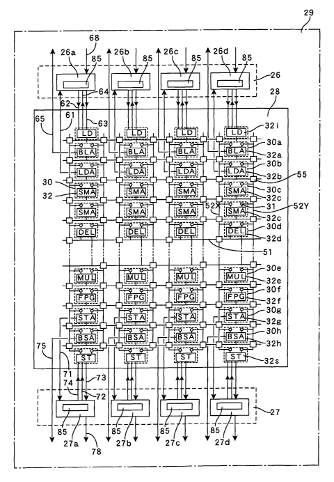
FIG. 3 shows an arrangement of a partial configuration 29 of AAP
20 comprising the matrix unit 28 and the small-capacity RAMS 26a to
26d and 27a to 27d of the present embodiment. In the present
2o invention, the matrix unit 28 is a system corresponding to the processing
unit in which data paths or data flows are reconfigurable or changeable.
The matrix unit 28 comprises a plurality of elements 30 that are
operation units, with these elements 30 being arranged in an array or
matrix so as to form four lines in the vertical direction. Between these
2s elements 30, the matrix unit 28 also comprises row wiring sets 51 that
extend in the horizontal direction and column wiring sets 52 that extend
in the vertical direction. The column wire sets 52 include a pair of wire
sets 52x and 52y that are composed of the wires in the column direction
2i
CA 02451003 2003-12-16
on the left and right sides, respectively, of the operation units 30, with
data being supplied to the individual elements 30 by these wire sets 52x
and 52y.
Switching units 55 are disposed at intersections between the row
s wire sets 51 and the column wire sets 52, with each switching unit 55
being able to switch and connect any of the channels of the row wire set
51 to any of the channels of a column wire set 52. Each switching unit
55 comprises a configuration RAM that stores settings, and by having the
content of the configuration RAM rewritten according to data supplied
io from the processor unit 11, the connections between the row wire set 51
and the column wire set 52 can be dynamically controlled as desired.
Accordingly, in the matrix unit 28 of the present embodiment, a
configuration of at least one data flow that is formed of all or parts of the
plurality of elements 30 by connecting the wire sets 51 and 52 can be
Is dynamically changed as desired.
Each element 30 comprises a pair of selectors 31 that respectively
select input data from the pair of column wire sets 52x and 52y and an
internal data path 32 that performs a specified arithmetic and/or logical
operation process on the selected input data "dix" and "diy" and outputs
20 output data "do" to the row wire set 51. Elements 30 with internal data
paths that execute different processes are arranged on different rows in
the matrix unit 28 of the present embodiment. The row wire sets 51
and column wire sets 52 also comprise wires for transferring carry signals.
The carry signals can be used as signals that show a carry or as signals
2s that show true or false, and in the matrix unit 28, these carry signals are
used for controlling the arithmetic operations and logic operations of each
element 30 and for transferring results to other elements 30.
First, the elements 30 that are arranged on the first row comprise
22
CA 02451003 2003-12-16
data path units 32i that are suited to processing that receives data from
the input buffer 26. If these data bus units ("LD") 32i for load
operations simply receive an input of data, logic gates are not required,
and data is simply received via the load bus 22 and is outputted to the
s row wire set 51. In the matrix unit 28, the data path units 32i for load
operations each have a function for stopping the processing of the data
flow to which the element 30 including this data path unit 32i is
connected when the stop signal 62 is received from the RAM arbitrating
unit 85 of the input RAM 26. Also, the data path units 32i for load
io operations also each have a function for outputting the stop signal 64 to
the arbitrating unit 85 of the corresponding input RAM 26 when the data
flow to which the element 30 including the data path unit 32i is
connected stops due to an internal factor in the matrix unit 28 or an
output-side factor.
Is The elements 30a that are arranged on the second row are
elements for writing data from the external RAM 2 into the input RAMs
26a to 26d of the input buffer 26, and correspond to the second address
outputting sections. Accordingly, these elements 30 each comprise a
data path portion or unit 32a with an internal data path that is suited to
2o generating an address (second address) for block loading. Such data
path units 32a are called BLAB (Background Load Address Generators).
FIG. 4 shows an example of the data path unit 32a that comprises an
address generator 38 composed of a counter, etc., with an address being
outputted from this address generator 38 as the output signal "do". The
2s output signal "do" is supplied via the row wire set 51 and the column
wire set 52 as it is or after processing by other elements 30 to a data
path unit 32 as the input signal "dix" or "diy", one of the supplied
addresses is selected by a selector "SEL", and outputted via a flip-flop
23
CA 02451003 2003-12-16
"FF" from the matrix unit 28 to the external access arbitrating unit 25 as
the input write address data 65.
Like all of the elements 30 that compose the matrix unit 28, the
elements 30 that generate these addresses comprise a configuration RAM
s 39 for setting conditions of an address generator 38 and selector SEL.
The data in the configuration RAM 39 is set by a control signal 18 from
the basic processor 11.
FIG. 5 shows one example of the address generating circuit 38.
This address generator 38 comprises a plurality of counters 38a and an
to adder 38b that performs some operations on the outputs of these
counters 38a and outputs the result as an address. As shown in FIG. 6,
each of the counters 38a comprises a combination of an arithmetic logic
unit ALU 38c and a comparator 38d, with it being possible to set an ADD,
SUB, bit shift, OR, XOR, or a combination of these operations in the ALU
is 38c. The counters 38a each have a function as a function generating
circuit that generates a value every time the clock signal rises. The
functions of the counters 38a can be set by the processor unit 11 via the
configuration RAM 39.
The control signal "en" of the ALU 38c can be set by a carry signal
20 "cy" supplied from another counter 38a and the output of the comparator
38d can be transmitted to another counter 38a as the carry signal "cy".
By using the carry signal in this way, the state of another counter 38a
can be set according to the state of a counter 38a and a desired address
can be generated. Also, though not shown in the drawing, the control
2s signal "en" of the counter 38a can be set according to the carry signal
"cy" supplied from another element 30 and can be transmitted to another
element 30.
The element (BLA) 30a that outputs the input write address data
24
CA 02451003 2003-12-16
65 has a construction of the data path unit 32a including an address
generating circuit 38 that is suited to the generation of addresses, with it
being possible to control the processing content of the address
generation from the processor 11 via the configuration RAM 39. It is
also possible to freely set how the element (BLA) 30a is related to the
other elements 30. The plurality of counters 38a that are included in the
BLA 32a are 32-bit counters, for example, and can generate an address
for DMA transfer from the external memory 2 to the input RAMs 26a to
26b that are local store buffers.
to The elements 30b arranged on the third row in FIG. 3 comprise
data path units 32b that generate input readout addresses 61 for loading
desired data from each of the input RAMS 26a to 26d into the matrix unit
28, and correspond to the first address outputting sections. The data
path unit 32b is called an LDA (Load Address Generator). The
construction of these data path units 32b is fundamentally the same as
the construction of the data path units 32a described above that
generate addresses, except that the data path units 32b output 16-bit
addresses, not 32-bit addresses like the data path units 32a.
Accordingly, the fundamental configuration of the data path units 32b is
2o as shown in FIG. 4.
One example of the address generating circuit 38 included in each
LDA 32b is shown in FIG. 7. This address generator 38 comprises four
16-bit counters 38a and generates an address for transferring data from
the input RAMS 26a to 26b, which are the local store buffers, to the
matrix unit 28. The control signal "en" of the counter 38a can be set by
the carry signal "cy" supplied from another element 30 and is constructed
so that the control signal "en" can be transmitted to another element 30.
Data is supplied from the input RAMs 26a to 26d to the matrix unit 28
CA 02451003 2003-12-16
according to the input readout address data 61 outputted from this
element 30, with this data being processed in some operations
performed by another logic or operation element that composes the
matrix unit 28.
s The elements 30c that are arranged on the fourth and fifth rows
comprise data path units ("SMA") 32c that are suited to arithmetic
operations and logic operations. As one example, these data path units
32c comprise a shift circuit, a mask circuit, an ALU and a configuration
RAM 39 for setting the operation to be executed by the ALU.
to Accordingly, the input data "dix" and "diy" can be subjected to operations
such as addition, subtraction, a comparison, a logical AND or a logical OR
according to an instruction written by the processor 11, with the result
being outputted as the output data "do".
The elements 30d that are arranged on the next row down
is comprise data path units ("DEL") 32d that are suited to processing that
delays the timing at which data is transferred. As one example, a data
path composed of a combination of a plurality of selectors and flip-flop
FFs is provided in these data path units 32d, and by having the input
data "dix" and "diy" take a path that is selected by the selectors
zo according to the data in the configuration RAM 39, the input data "dix"
and "diy" are delayed by a desired number of clocks and then outputted
as output signals "dox" and "doy"
The elements 30e that are arranged on the next row down
comprise data path units ("MUL") 32e that comprise multipliers or the
2~ like and are suited to multiplication. Elements that comprise data path
units 32f for an interface with the FPGA unit 14 that is provided on the
outside of the matrix unit 28 are also provided as another kind or type of
elements 30f, with these elements 30f being able to continuously
26
CA 02451003 2003-12-16
perform processing that supplies data to the FPGA unit 14 and returns
the data to the matrix unit 28 after processing.
Elements 30g and 30h that respectively comprise data path units
32g and 32h that are suited to generating store addresses are arranged
s further below the region correspond to the data processing section in
which the above types of elements are arranged. These data path units
32g and 32h have fundamentally the same construction as the data path
units 32b and 32a respectively that generate addresses and were
described above with reference to FIGS. 4 to 7. The elements 30g that
to comprise the data path units 32g are the first address outputting sections
and output the output write addresses 71 for writing data outputted from
the matrix unit 28 into the output RAMS 27a to 27d. Therefore, the data
outputted from the data processing systems using the various types of
elements 30c to 30f that are described above is written into the output
Is RAMs 27a to 27d. Each data path unit 32g is called an STA (Store
Address Generator) and has the same configuration as the LDA 32b.
The elements 30h that comprise the data path units 32h and are
arranged below these elements (STA) 30g are the second address
outputting sections and output the output readout addresses 75 for
2o reading out data from the output RAMs 27a to 27d and writing data into
the external RAM 2 so that data processed by the matrix unit 28 is
written into the external RAM 2. Each data path unit 32h is called a BSA
(Background Store Address Generator) and has the same construction as
the BLA 32a.
2s Elements 30 comprising data path units 32s that are suited to the
outputting of data for storing are arranged on the final row. These data
path units 32s are called "ST", with it being possible to use data path
units with almost the same construction as the data path units 32c for
27
CA 02451003 2003-12-16
arithmetic operations. Also, in the present embodiment, each data path
unit 32s for outputting is provided with a function for stopping the
processing of the data flow that is connected to the element 30 including
the data path unit 32s when a stop signal 74 is received from the
s arbitrating unit 85 of the output RAM 27.
In this way, the matrix unit 28 of the present embodiment
comprises elements 30a with internal data paths (BLA) 32a that generate
addresses for inputs (block loads) of data from the external RAM 2 into
the input RAMs 26a to 26d and elements 30b with internal data paths
Io (LDA) 32b that generate addresses for inputs of data into the matrix unit
28 from these input RAMS 26a to 26d. The matrix unit 28 also
comprises elements 30g with internal data paths (STA) 32g that
generate addresses for outputs of data from the matrix unit 28 to the
output RAMs 27a to 27d and elements 30h with internal data paths
Is (BSA) 32h that generate addresses for outputs (block loads) of data in
the output RAMs 27a to 27d to the external RAM 2. These elements 30a,
30b, 30g, and 30h each have a data path that is suited to the generation
of the addresses mentioned above, with it being possible to change the
configurations and functions of the data path by rewriting the data in the
2o configuration RAM 39. The connections with the other elements 30 in
the matrix unit 28 can also be changeable by changing the connections of
the row wire sets 51 and the column wire sets 52. Accordingly, data for
address generation can be provided from the processor 1l and/or from
other elements 30 in the matrix unit 28 and the timing at which
Zs addresses are generated can be flexibly controlled.
In this way, according to a variety of conditions and/or
constructions, data can be loaded from the external RAM 2 and input
RAMs 26a to 26d that are used as caches. Separate to this processing,
2~
CA 02451003 2003-12-16
data can also be loaded into the matrix unit 28 asynchronously and/or
independently from the input RAMs 26a to 26d according to different
conditions. In addition, the elements 30a and 30b are independent, so
that such processing can be executed in parallel. Accordingly, the
s plurality of input RAMS 26a to 26d are storage sections where inputting
and outputting can be performed independently.
Since each of the input RAMs 26a to 26d has a dual-bank
configuration, inputting and outputting can be performed in parallel for
each of the input RAMS 26a to 26d, so that with this configuration, the
to inputting and outputting of data into and out of each of the input RAMs
26a to 26d can be performed extremely efficiently. This is also the case
for each of the output RAMs 27a to 27d, those are also storage sections
where inputting and outputting can be performed independently, and
inputting and outputting into and from each of the output RAMs 27a to
Is 27d can be performed independently and in parallel. Accordingly, in this
system, inputs and outputs of data can be performed extremely
efficiently for the RAMs 26a to 26d and 27a to 27d that operate as
caches.
The matrix unit 28 of the present embodiment comprises the
2o elements 30a, 30b, 30g, and 30h with the data path units 32a, 32b, 32g,
and 32h that are fundamentally suited to the generation of addresses,
with the operations of these elements being determined according to
instructions from the basic processor 11. This is to say, according to
instructions that are supplied via the control bus 18 from the basic
2s processor 11, which is the control unit, the circuit for accessing the RAMs
26a to 26d and 27a to 27d, which are the first memory, is determined
and the circuit for accessing the DRAM that is the main memory (the
second memory) is also determined.
29
CA 02451003 2003-12-16
In addition, a circuit for controlling the accesses to these memories
is configured in the matrix, so that it is extremely easy to directly or
indirectly reflect the conditions on the inside of the matrix unit 28, for
example, the configuration of the data flows, the processing results of
the data flows, and also the results of processing that uses other
elements of the matrix unit 28, in the operation of these circuits. The
elements 30a, 30b, 30g, and 30h are not only suited to the generation of
addresses but also be freely wired to other elements in the matrix unit 28
by the wires 51 and 52 in the same way as the other elements. For this
io reason, the outputs from the elements 30a, 30b, 30g, and 30h can be
controlled by changing the parameters and/or the processing content of
the elements 30a, 30b, 30g, and the 30h according to a data flow or data
flows that are configured by the other elements that form the data
processing section in the matrix unit 28 and/or the software that is
Is executed by the data processing section. By constructing a data flow
using the other element in addition to the elements 30a, 30b, 30g, and
30h, the functions of the other elements can also be used for generating
addresses. Therefore, the access method for accessing the RAMS 26a to
26d and 27a to 27d that are the first memory that composes the cache
2o system and the access method for accessing the DRAM 2 that is the main
memory (second memory) can be flexibly determined according to
conditions on the inside of the matrix unit 28, for example, the
construction of the data flows and the processing results.
The matrix unit 28 is reconfigurable according to control from the
25 basic processor 11, so that the internal data paths and functions of the
elements 30a, 30b, 30g, and 30h that generate addresses can also be
dynamically reconfigurable and the connections with other elements can
also be dynamically reconstructed. It is also possible to provide the
CA 02451003 2003-12-16
function for instructing reconfiguration of the connections within elements
or between elements on the inside of the matrix unit 28. When the
configurations of data flows or data paths are rearranged by changing
the connections with the other elements 30 in the matrix unit 28
s according to the processing content executed by the matrix unit 28, it is
also possible to change the configurations that input and output data into
and out of the buffer 26 composed of the input RAM and the buffer 27
composed of the output RAM.
For this reason, it is possible to use a configurtion that is optimally
to suited to the processing executed by the matrix unit 28 for the cache
system that inputs and outputs data to and from the input buffer 26 and
the output buffer 27, so that the hit rate of the cache can be raised, and
the frequency of rewrites of data in the cache can be reduced. It is also
possible to reconfigure the insides of the elements 30a, 30b, 30g, and
is 30h that generate addresses and the data paths related to these
elements on an element-by-element basis and to rearrange the cache
system separately for each of the RAMs 26a to 26d and 27a to 27d. This
makes the present invention extremely flexible. Accordingly, before a
data processing system or systems are configured in the matrix unit 28
2o from the other elements 30, it is possible to realize a data input
configuration that is suited to the data processing system to be
configured and commence data loads. On the other hand, after the data
processing system has been reconfigured for other processing, the data
outputting configuration can be maintained for outputting continuously
2~ the data processed by the data processing system that has been already
reconfigured. In this way, processing that was inconceivable with
conventional techniques can be executed with great flexibility. This is to
say, the processing performed for the RAMS 26 and 27 that are the first
31
CA 02451003 2003-12-16
memory and the DRAM 2 that is the second memory can be executed as
desired independently of other elements and data flows or alternatively
as part of the processing of other elements or data flows. It is also
possible to make the elements 30a, 30b, 30g, and 30h that generate
s addresses to operate relationally or cooperatively, to make a plurality of
elements 30a and/or 30b operate relationally or cooperatively, and to
have the matrix unit 28 use the plurality of RAMs 26 as a single high-
capacity cache.
Also, it is possible for the element 30a to perform a process that
to outputs the input write address 65 and writes data from the RAM 2 when
the input RAM 26a becomes empty, while the element 30b performs a
process that loads data into the matrix unit 28 when there is data in the
RAM 26a. The elements 30a and 30b can be made to operate
independently and in parallel, so that data in the external RAM 2 can be
is prefetched into the input RAM 26a without wasting the processing time of
the data processing system. If the element 30a controls the address at
which data is inputted from the external RAM 2, the processing in a data
processing system composed of the element 30b and the matrix unit 28
can proceed with only an address in the internal RAM 26a. If a data
2o flow-type processing system is defined using a plurality of other elements
30 in the matrix unit 28, data processing can proceeded in the matrix
unit 28 with only the data and without using an address.
It is also possible to configure a system in which a virtual address
is outputted from a data processing system in the matrix unit 28 and the
2s element 30b converts this virtual address into a physical address in the
input RAM 26a and supplies data, with the element 30a converting the
virtual or physical address into a physical address in the external RAM 2
and loading the data from the external RAM 2 when the data is not in the
32
CA 02451003 2003-12-16
input RAM 26a.
It is also possible to configure a system where the element (BLA)
30a generates an address from data inputted from the input RAM 26b,
with this address being used to load data from the external RAM 2 into
s the input RAM 26a. Accordingly, completely indirect addressing control
can be performed by merely the mechanism that performs inputs and
outputs for the input RAM 26 and the output RAM 27 independently of
the data processing system constructed in the matrix unit 28. It is also
possible to realize a multilevel cache system by linking the operations of
to the plurality of input RAMs 26a to 26d, the output RAMs 27a to 27d, and
also the access arbitrating unit 25.
The AAP 20 of the present embodiment is provided with four input
RAMS 26a to 26d and four output RAMs 27a to 27d that correspond to
the elements 30 that are arranged in four columns. Accordingly, the
is input RAMs 26a to 26d and the output RAMs 27a to 27d can be used as
individual cache memories that respectively correspond to the plurality of
data processing systems configured with the other kinds elements 30 in
the matrix unit 28. When a plurality of jobs and/or applications are
executed by the matrix unit 28, the input RAMs 26a to 26d and the
20 output RAMs 27a to 27d can be used separately as optimal caches for
these jobs and/or applications. The elements 30 are arranged in four
columns, though the data processing systems configured with these
types of elements 30 are not limited to four. If three or fewer data
processing systems are configured in the matrix unit 28, the capacity of
2s the cache memory used by one data processing system can be increased
by assigning a plurality of RAMS out of the input RAMs 26a to 26d and
the output RAMs 27a to 27d to one data processing system. When there
are five or more data processing systems are configured, one RAM is
33
CA 02451003 2003-12-16
assigned to a plurality of data processing systems as a cache memory.
In this case, at the worst, the same condition may be occurred as cache
processing for multitasking that is performed in a modern CPU of data
processing system that shares a RAM.
s As shown in outline in FIG. 8, a system LSI 10 that is the
integrated circuit device or processing device of the present invention
comprises a configuration or assembly 29 including a matrix portion or
part that is the processing unit and a small-capacity RAM, with addresses
that are outputted to the external RAM 2 from the matrix part being
io supplied to the external RAM 2 via the arbitrating unit 25. An address
generating mechanism that controls the inputting and outputting of data
into and out of the small-capacity RAM is realized by the matrix port
where data flows can be reconfigured, so that the architecture that
controls the small-capacity RAM that functions as a cache memory can
Is also be reconfigured and so can be changed to an optimal construction
for the software executed by the matrix unit. Accordingly, with the
system LSI 10 that is the integrated circuit device or processing device of
the present invention, the small-capacity RAM can be used as a cache
memory in the most efficient manner for the hardware environment and
2o the processing content of the software that is to be executed. For a
variety of software programs are executed, a cache memory and a circuit
for controlling this cache memory can be configured so that a higher hit
rate is obtained. Accordingly, it is possible to provide an integrated
circuit device or processing device (system LSI or ASIC) in which no
2s overloads are caused by inputs into and outputs from the cache memory
for a variety of software is executed.
The external memory that can be controlled by the system LSI 10,
that is the second memory, is not limited to RAM. The device used as
34
CA 02451003 2003-12-16
the external memory for the input RAM and/or the output RAM is not
limited to a storage device such as a RAM, ROM, or even a hard disk
drive, and includes any device that can input or output data when an
address is indicated. As one example, as shown in FIG. 9, when the LSI
s 10 controls a large-capacity RAM 2 and a peripheral device 3, such as a
printer or a display, as an external memory, the elements BLA 30a and
BSA 30h that perform block loads for the matrix unit 28 may generate
physical addresses that are assigned to the peripheral device 3.
Also, as shown in FIG. 10, it is possible to provide the LSI 10 that
to controls a plurality of large-capacity RAMs 2 and peripheral devices 3 via
a plurality of bus controllers. In this case, modifications, such as the
provision of a plurality of arbitrating units 25, may be applied. Also, a
large-capacity RAM 2 may be implemented inside the LSI 10, and it is
also possible to use a construction where the large-capacity RAM 2 is
is used as a cache memory for the peripheral devices 3. The large
capacity RAM 2 may also be used as a code RAM of the processor 1l.
The above explanation describes one example of the construction
of the matrix unit or part 28, though the present invention is not limited
to this construction. In the above description, operation elements that
2o include the special-purpose data paths 32 suited to special-purpose
processing such as address generation, arithmetic operations, logic
operations, multiplications, and delays are described as the elements
with, though the functions of the data paths and their configurations are
not limited to the examples given above. By arranging elements
2s including data paths with some functions that are suited to the
applications executed by the LSI 10, which is the integrated circuit device
or data processing device of the present invention, in a matrix or in an
array, it is possible to provide a processing unit in which data flows can
3~
CA 02451003 2003-12-16
be changed or reconfigured. A plurality of matrix units 28 may be
implemented or arranged, with the plurality of matrix units being
arranged on the same plane or in three dimensions, so that an integrated
circuit device comprising an even larger number of elements can be
s constructed. Also, the integrated circuit device of the present invention
is not limited to an electronic circuit and can be adapted to an optical
circuit or an optoelectronic circuit.
While the present invention is described above by means of an
example in which an AAP 20, a basic processor 11, and a bus control
Io unit 15 are incorporated in a system LSI 10, the range of the
components to be provided as a single chip depends on conditions such
as the applications to be implemented. The AAP 20 may also be
provided as a single chip, or alternatively the part 29 that includes the
RAMs 26 and 27, which form the cache, and the matrix unit 28 may be
is packaged into a single chip. It is also possible to provide a larger
system LSI or ASIC comprising a plurality of AAP units or other special
purpose circuits in addition to the basic processor 11.
As shown in FIG. 11, the integrated circuit device or processing
device of the present invention can also be realized by using an FPGA as
2o a processing unit in place of the matrix unit 28 and, in the FPGA, in
addition to the data processing section, the first and second address
outputting sections of the present invention can be programmed or
mapped for using the input RAMS 26 and the output RAMs 27 as caches.
An FPGA is an architecture where the configuration of data paths that
2s have wide applicability can be changed at the transistor level. Research
is also being performed into integrated circuit devices where the data
paths or data flows can be reconfigured using medium-scale basic
functional units that are of the same construction, the basic functional
36
CA 02451003 2003-12-16
units consisting the same kinds of elements (though not at the transistor
level) but executing various processes according to an instruction set.
In a processing unit having this kind of architecture, the integrated circuit
device and processing device of the present invention can also be
s realized by configuring (or indicating the configuration of), in addition to
a data processing section, a first and second address outputting section
that have the input RAM 26 and the output RAM 27 function as caches.
Unlike the architecture where basic units of the same construction
are aligned, an architecture based on the matrix unit described above
to comprises a plurality of types of elements, each type of element including
different internal data paths. Since this is not an architecture that needs
to have wide applicability on a transistor level, the packing density can
be raised and a compact, economical system can be provided. Also,
since each of the elements 30 comprises a data path unit 32 that is
Is dedicated to special-purpose processing, a large reduction can be made
in the redundancy in the construction. Compared to an FPGA or another
processing unit in which basic processing units of the same construction
are arranged, a large increase can be made in processing speed and the
AC characteristics can also be improved. Also, since space is used more
2o efficiently, a compact layout can be used, and the lengths of the wires
can also be reduced. Accordingly, the architecture including matrix is
suited to an integrated circuit device or processing device that makes full
use of the efficient cache construction disclosed by the present invention
that makes possible to provide a low-cost processing device with higher
2s speed processing.
Furthermore, unlike an FPGA where circuits are mapped at the
transistor level, i changing the combination of elements 30 that include
the data path units 32 which are suited in advance to special-purpose
37
CA 02451003 2003-12-16
processing has the merit that configurations and functions of the data
processing units, that is the data processing systems configured in the
matrix unit 28, can be changed in a short time that in most cases is one
clock. Also, in each element 30, the functions of the selectors and logic
s gates, such as the ALU, that compose the data path unit 32 can be set
independently by the processor 11 via the configuration memory 39, so
that the data path unit 32 of each element 30 can be flexibly changed
within the range of functions that the data path unit is serviced.
Accordingly, in the matrix unit 28 of the present embodiment, the range
to of functioning that can be executed by data flow-type data processing is
extremely wide. It is also possible to select and arrange suitable types
of operation units 30 for the application, such as network processing or
image processing, for which the LSI 10 is to be used, which makes it
possible to provide an integrated circuit device with even higher
is mounting efficiency and processing speed.
As described above, the present invention forms the first address
outputting section and second address outputting section that control a
first memory which can be used as a cache memory in a processing unit
in which the data flows are changeable. This means that the
2o configuration of the cache system can be dynamically reconfigured to an
optimal configuration for the configuration of the data processing section
and the software that is executed by the data processing section. When
a variety of software is executed, a cache system with a higher hit ratio
can be constructed. Accordingly, it is possible to provide an integrated
2s circuit device that executes a variety of software or applications in a
shorter processing time.
Industrial Applicabilitx
38
CA 02451003 2003-12-16
The processing unit and integrated circuit device of the present
invention can be provided as a system LSI, an ASIC, or the like that can
execute a variety of data processing. The processing unit and integrated
circuit device of the present invention are not limited to electronic
circuits,
s and may be adapted to optical circuits or optoelectronic circuits. The
integrated circuit device of the present invention can execute data
processing at high speed using hardware that can be reconfigured, and
so is suitable for a data processing device that performs processing, such
as network processing and image processing, where high-speed and real-
to time processing is required.
39