Note: Descriptions are shown in the official language in which they were submitted.
CA 02451463 2003-12-18
WO 02/103311 PCT/US02/19195
METHOD AND APPARATUS FOR READOUT OF COMPOUND MICROBOLOMETER ARRAYS
Field of the Invention
This invention relates generally to a microbolometer focal plane array, and
more particularly pertains to an improved readout technique for the
microbolometer
array.
Background
Thermal infrared detectors are detectors, which operate by sensing the
heating effeet of infrared radiation. Thermal detectors generally do not need
to be
cooled below room temperature, which gives them an important practical
advantage.
Thermal infrared detectors that operate at room temperature have been l~nown
for
200 years, but recently the availability of integrated circuit and
rnicromachining
technology has greatly increased interest in this field. It is now practical
to
manufacture an array containing many thousands of thermal infrared detectors,
which operates well at room temperature.
A bolometer is a thermal radiation detector that operates by absorbing
incident electromagnetic radiation (typically infrared radiation), converting
the
absorbed infrared energy into heat, and then indicating the resulting
temperature
change in the detector by a change in its electrical resistance, which is a
function of
temperature. A microbolometer is a small bolometer, typically a few tens of
microns
in lateral size. Microbolometer infrared imaging systems are typically
designed to be
sensitive to long-wave infrared, typically in a wavelength range of about 8-12
micrometers. A two-dimensional array of such microbolometers, typically
120x160
microbolometers, can detect variations in the amount of radiation emitted from
objects within its field of view and can form two-dimensional images
therefrom. A
typical array can have more than 80,000 microbolometers. Linear arrays of
microbolometers may similarly be formed to form line images. In such large
arrays
of microbolometers, it is necessary to measure the resistance of all of the
individual
1
CA 02451463 2003-12-18
WO 02/103311 PCT/US02/19195
microbolometers in the array without compromising lie si'gna'l"'t'o iioise'-
ratio'of~'he~
microbolometers. Because it is impractical to attach thousands of electrical
wires to
such an array to measure all the microbolometer electrical resistances in the
array,
microbolometer arrays are typically built on a monolithic silicon called a
"read out
integrated circuit" (ROIC) which is designed to measure all the individual
microbolometer electrical resistances in the array in a short time, called the
"frame
time." The term "frame time" refers to a time in which a microbolometer array
produces each complete picture or image of an object being viewed. The frame
time
is typically around 1/30~h of a second, but it can be faster or slower than
the typical
time of 1/30th of a second. In order to allow the microbolorneter array to
respond
adequately to time-dependent changes in the detected infrared radiation, the
thermal
response time of each microbolometer is typically adjusted, by power design,
to be
about the same value as the frame time.
A typical method used by the ROIL to measure the electrical resistance of all
the microbolorneters in the array is to apply a "bias pulse" of electrical
voltage (or
current) to each microbolometer in the array, and to measure a resulting
signal
current (or voltage). It is more common to apply a voltage bias pulse to each
rnicrobolometer in the array and to measure a resulting current signal from
each
microbolometer in the array during each frame time. In large arrays such as
the one
included in the ROICs, it is usual to apply such bias pulses to more than one
microbolometer simultaneously, and to measure the resulting signal currents
simultaneously. However, it becomes difficult to read each of the
microbolometers
in the array within the frame time. Therefore, it is advmtageous to divide
such large
arrays into several smaller arrays to ease the reading process of large
arrays. In such
cases, each smaller array would be readout as if it were a separate array
using its own
data readout port and feeding data to a corresponding measurement circuit
associated
with each smaller array. The division of the large arrays need not be a
physical
division.
However, such a scheme of dividing the array into smaller arrays with each
smaller array having its own measurement circuit to ease the reading of the
larger
array can produce undesirable deficiencies in the produced image. This is
generally
2
CA 02451463 2003-12-18
WO 02/103311 PCT/US02/19195
due to different drifts in the output signals of the smaller arrays~iri~ucec~-
by'c'~iariges
in different measurement circuit characteristics, such as offset voltage,
offset current,
and gain.
Therefore, there is a need in the art to design and operate a large array
including multiple smaller arrays having their own data readout ports such
that they
do not produce the undesirable pattern artifacts in the produced image due to
drifts
in measurement circuits associated with each of the smaller arrays.
Summary of the Invention
The present invention provides a technique to reduce undesirable pattern
artifacts in an image produced by a microbolometer array including multiple
smaller
arrays. This is accomplished by applying a bias pulse to each of the
microbolometers
in the multiple smaller arrays and measuring a resulting signal corresponding
to the
applied bias pulse for each of the microbolometers using multiple measurement
circuits associated with the multiple smaller arrays during the frame time.
Further,
the technique requires applying one or more known bias pulses (calibration
signals)
to the multiple measurement circuitry associated with the smaller arrays
during the
frame time and measuring one or more resulting calibration signals
corresponding to
the applied one or more known bias pulses. Thereafter the technique requires
computing an offset parameter fox each of the multiple smaller arrays based on
the
corresponding measured one or more resulting calibration signals and
correcting the
measured resulting signal using the associated computed offset parameter to
produce
an output signal that significantly reduces the undesirable pattern artifact
in the
image.
Other aspects of the invention will be apparent on reading the following
detailed description of the invention and viewing the drawings that form a
part
thereof.
3
CA 02451463 2003-12-18
WO 02/103311 PCT/US02/19195
Brief Description of the Drawings
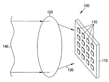
Fig~.~re 1 illustrates the use of a microbolometer array in an imaging system.
Figure 2 illustrates a typical ROIC circuit including multiple smaller arrays
to
ease the readout process.
Figure 3 illustrates a typical readout circuit including an integrator and an
A/D converter used to convert an output signal to a digital signal value from
each of
the multiple smaller arrays.
Figure 4 illustrates a method of reducing undesirable artifacts produced when
using multiple smaller arrays having their own readout circuitry.
Figure 5 illustrates major components of an infrared radiation detector
apparatus and their interconnections according to the present invention.
4
CA 02451463 2003-12-18
WO 02/103311 PCT/US02/19195
Detailed Description
This document describes a technique to reduce undesirable deficiencies in an
image
produced by a microbolometer array including multiple smaller arrays coupled
to
respective multiple measurement circuits.
Figure 1 illustrates one embodiment of using a microbolometer array 110 in an
imaging system 100. The imaging system 100 further includes an infrared-
transmitting lens
120. The array 110 can be a one or two dimensional array. The array 110 is
formed on a
monolithic silicon read out integrated circuit (ROIC) 115. In the embodiment
shown in
Figure 1, the array 110 is disposed in the focal plane of the infrared-
transmitting lens 120,
such that the rays of infrared radiation 130 are focused onto the focal plane
to produce an
image of a distant obj ect or scene 140, in the same way that a photographic
film produces
an image when placed in the focal plane of a camera lens. The heating effect
of the focused
image causes temperature changes in individual microbolometers in the array
110. This
temperature change in each of the microbolometers induces a change in
resistance value in
each of the microbolometers in the array 110. The ROIL 115 interrogates each
microbolometer in the array 110 to measure the change in resistance in each of
the
microbolometers in the array 110. The change in resistance in each of the
microbolometers
is measured within a frame time. Generally, the frame time is around 1/30th of
a second.
The thermal response time of each microbolometer in the array is generally
tailored to be
approximately equal to the frame time. The above-indicated measurement of the
change in
resistance in each of the microbolometers is repeated every frame time so that
a real-time
image ofthe scene and/or object 140 being viewed is displayed.
Figure 2 illustrates one example embodiment of a ROIC 115 used in forming the
microbolometer array 110 including two smaller arrays 280. Each microbolometer
in the
array 110 is represented as an electrical resistor 220. Associated with each
microbolometer
220 in the array 110 is a field-effect transistor (FET) 230. The
microbolometers 220 and
the FETs 230 are interconnected as shown in Figure 2 by thin-film metallic
conductors
240. The ROIL 115 further includes column and row shift registers 250 and 260.
The
5
CA 02451463 2003-12-18
WO 02/103311 PCT/US02/19195
column shift register 250 applies control voltages to columns of the array
110, and the shift
register 260 applies control voltages to a row multiplexer 270. A global bias
voltage
VDDR is applied to all the microbolometers in the array 110. The two output
signal lines
285 associated with each of the two smaller arrays 280 are held at zero volts
by two
measurement circuits 290.
In operation, the ROIC 115 typically applies control voltages so that only one
microbolometer in each of the two smaller arrays 280 has an applied VDDR
across it, and a
signal current flows along the corresponding thin-film row metallic conductor
240, through
the multiplexer 270, and out to the associated output signal lines 285.
Additional current is
supplied from current sources 291 associated with each of the multiple smaller
arrays 280
to bring the net output current substantially close to zero. The current
sources 291 can
apply different bias current values for different microbolometers 220 in the
array 110
during each time interval the microbolometers 220 are being biased, so that
the output
current remains close to zero even if the resistance of different
microbolometers have
slightly different resistance values, due to small fabrication variations
between different
microbolometers 220 in the array 110.
The signal zeroing process called "coarse non-uniformity correction" together
with
other methods and apparatus to correct for coarse non-uniformity are taught in
U.S.Patent
No. 4,752,694. The output signals 294 are input into associated integrators
and A/D
converters 296 to convert the signals 294 to a digital signal value 298.
Calibration circuits
292 for applying calibration bias pulses are coupled to the two measurement
circuits 290,
so that the respective output signals also include calibration signals to
correct for unwanted
drifts in the respective integrators and A/D converters 296.
Figure 3 illustrates a typical measurement circuit 290 coupled to a digital
signal
processor 340. The output signals 285 are integrated using a capacitor 320 and
an amplifier
310 until discharged by a switch 330 during a frame time. The signal 294 is
converted to a
digital signal value 298 using the A/D converter 296. A digital signal
processor 340
includes a digital memory 350, and a correction circuit 360. The digital
memory 350 holds
6
CA 02451463 2003-12-18
WO 02/103311 PCT/US02/19195
correction values for each microbolometer in the respective smaller array 280.
The
correction circuit 360 generates the final output signal 365 using the digital
signal value
298 and the associated correction value stored in the digital memory 350. The
corrections
are typically "fine offset corrections", which generally removes small zero-
error signals.
The corrections can also include "gain correction," which correct for
differing sensitivities
between different microbolometers 220 in the array 110. The corrections can
further
include "dead pixel replacement," which is a replacement of signals from
poorly operating
microbolometers in the array 110 with signal values derived from neighboring
microbolometers. Corrections can also include corrections for contrast,
brightness, and/or
pseudocolor to produce an image that can more readily be perceived by an
observer.
Figure 4 illustrates an overview of one embodiment of the process 400 of the
present invention. As illustrated in step 410, this process applies a separate
bias pulse
during a frame time to each of the microbolometers in a microbolometer array
divided into
multiple smaller arrays. The frame time is the time it takes for the array to
produce one
complete image of an object being viewed by the array. The bias pulse can be a
voltage
bias pulse. The bias pulse can have time duration of in the range of about 0.1
to 20
microseconds. In some embodiments, applying the bias pulse can include
applying multiple
bias pulses so that they are substantially sequential and substantially equal
in magnitude
during the frame time. The multiple bias pulses can be in the range of about 2
to 100 bias
pulses.
Step 420 measures a resulting signal corresponding to the applied bias pulse
during
the frame time for each of the microbolometers in the smaller arrays using
measurement
circuitry associated with each of the smaller arrays. In some embodiments, the
resulting
signal is a current signal. Step 430 applies one or more calibration bias
pulses during the
frame time to each of the measurement circuitry associated with the smaller
arrays. Step
440 measures one or more resulting calibration signals corresponding to the
applied
calibration bias pulses during the frame tune. Step 4S0 computes correction
parameters for
each of the smaller arrays based on each of the associated measured resulting
calibration
7
CA 02451463 2003-12-18
WO 02/103311 PCT/US02/19195
signals. In some embodiments, correction parameters can be offset voltage,
offset current,
and/or gain correction. Step 460 corrects the measured resulting signal using
each of the
associated computed correction parameters to produce an output signal that has
a
substantially reduced undesirable deficiencies in the produced image between
the smaller
arrays. The process 400 includes repeating the above steps each frame time to
reduce
undesirable deficiencies in the produced image by each of the smaller arrays
including its
own measurement circuitry.
In some embodiments, the process 400 can further include applying a corrective
signal to each output signal to correct for resistance non-uniformity between
the
microbolometers in each of the smaller arrays to obtain a substantially more
uniform output
signal. In some embodiments, the substantially more uniform output signal
associated with
each of the microbolometers in the array is converted to a digital signal
value. In some
embodiments, the process 400 can also include passing each of the digital
signal values
associated with each of the microbolometers in the array through a digital
image processor
to correct for image defects. In some embodiments, image defects can include
offsets,
deficiencies, gain non-uniformities, and/or dead pixels.
Figure 5 illustrates major portions of an infrared radiation detector
apparatus 500
and their interconnections according to the present invention. The infrared
radiation
detector apparatus 500 includes a microbolometer array 110. The microbolometer
array
110 is further divided into multiple smaller arrays 280. In the example
embodiment shown
in Figure 5 the microbolometer array 110 is divided into two smaller arrays.
The apparatus
500 further includes first and second timing circuits 510 and 520,
respectively. The
apparatus 500 further includes multiple calibration and measurement circuits
292 and 290,
respectively corresponding to each of the smaller arrays 280. The first timing
circuit is
coupled to the array 110. The second timing circuit 520 is coupled to each of
the
calibration circuits 292. Further, the apparatus 500 includes an integrator
and an A/d
converter 296, and a digital image processor 340. The digital image processor
340 further
includes a correction circuit 360, and digital memories 350.
CA 02451463 2003-12-18
WO 02/103311 PCT/US02/19195
In operation, the first timing circuit 510 applies a bias pulse to each of the
microbolometers in the smaller arrays 280 during a frame time. In some
embodiments, the
bias pulse can include multiple bias pulses that are substantially equal in
magnitude. The
multiple bias pulses can also be applied such that they are substantially
equally spaced in
time. In some embodiments, the bias pulse is a voltage bias pulse. The bias
pulse can have
a time duration of 1 to 100 microseconds. The frame time is the time it takes
for the array
110 to produce a complete image of an object being viewed by the array 110.
The multiple measurement circuits 290 measure resulting signals associated
with
each of the applied bias pulses during the frame time. In some embodiments,
the resulting
signals can be current signals. The second timing circuit 520 applies one or
more bias
calibration bias pulses during the frame time to each of the measurement
circuits 290. Then
the measurement circuits 290 measure one or more resulting calibration signals
corresponding to the applied one or more calibration bias pulses. Then the
measurement
circuits 290 compute correction parameters for each of the smaller arrays
based on each of
the measured one or more resulting calibration signals. Further, the
measurement circuits
290 apply each of the computed correction parameters to the measured resulting
signal to
produce an output signal that reduces undesirable deficiencies in an image
produced by the
microbolometer array including multiple smaller arrays 280. The correction
parameters can
be an offset voltage, an offset current, and/or a gain correction.
In some embodiments, the integrator and A/D converter 296 convert the output
signal to a digital signal value for each of the microbolometers in the
smaller arrays 280. In
some embodiments, the digital image processor 340 including the correction
circuit 360
receives the digital signal value associated with each of the microbolometers
in the smaller
arrays 280 and corrects for image defects such as offsets, gain non-
uniformities, and/or
dead pixels. In some embodiments, the correction circuit 360 further applies a
corrective
electrical signal to correct for any resistance non-uniformity present in each
of the
microbolometers in the smaller arrays 280 to obtain a substantially uniform
output signal
9
CA 02451463 2003-12-18
WO 02/103311 PCT/US02/19195
value. The corrective electrical signals associated with each of the
microbolometers in the
array 110 are stored in the digital memories 350.
Conclusion
The above-described method and apparatus provides reduced undesirable
deficiencies in an image produced by a microbolometer array divided into
multiple smaller
arrays including their own measurement circuits.
The above description is intended to be illustrative, and not restrictive.
Many other
embodiments will be apparent to those skilled in the art. The scope of the
invention should therefore be determined by the appended claims, along with
the
full scope of equivalents to which such claims are entitled.