Note: Descriptions are shown in the official language in which they were submitted.
CA 02451882 2003-09-15
WO 02/073699 PCT/US02/07769
NANOFABRICATTON
Government Rights
This invention was made with govenunent support under U.S. Department of
Energy Grant No. DE-FG02-96ERA45612, U.S. National Science Foundation Grant
No. DMR-9809365, and U.S. National Science Foundation Grant No. CTS-9871782.
The government has certain rights in this invention.
Technical Field
The invention relates to fabrication of nanoscopic structures. W particular,
the
invention relates to functionalized nanoscopic structures on surfaces.
Bacl~ground
The fabrication of useful nanoscale devices has proved difficult. Approaches
based on porous aluminum oxide (AnoporeTM), ion-tracl~-etched polycarbonate
(NucleporeTM), ion-tracl~-etched mica, and other approaches, have been
attempted.
Examples of these are disclosed by Mitchell et al., in "Template-Synthesized
Nanomaterials in Electrochemistry", Electroanalytical C7zeTfZistny, A. J. Bard
and I.
Rubinstein, Eds., 21, (1999), 1-74; Strijl~ers et al., in "Structure and
Magnetization of
Arrays of Electrodeposited Co Wires in Anodic Alumina," J. App. Plays., 86,
(1999),
5141; Han et aL, in "Preparation of Noble Metal Nanowires Using Hexagonal
Mesoporous Silica SBA-15," CheJn. Mater., 12, (2000), 2068-2069; Whitney et
al., in
"Fabrication and Magnetic Properties of Arrays of Metallic Nanowires,"
Science, 261,
(1993), 1316; and in United States Patent No. 6,185,961 for "Nanopost arrays
and
process for malting same," to Tonucci et al.; and United States Patent No.
6,187,165
for "Arrays of semi-metallic bismuth nanowires and fabrication techniques
therefor,"
to Chien et al. These approaches result in materials which can be very
difficult or
impossible to pattern laterally and/or integrate. Other devices which can be
prepared
are macroscopic in scale, as disclosed in Uuted States Patent No. 6,187,164
for a
"Method for creating and testing a combinatorial array employing individually
addressable electrodes," to Warren et al.
CA 02451882 2003-09-15
WO 02/073699 PCT/US02/07769
Recently, companies such as Samsung and Hitachi have used carbon
nanotubes as field emission sources to make prototype field emission (FE)
displays.
FE devices based on carbon nanotube materials are disclosed in "Flat panel
display
prototype using gated carbon nanotube field emitters," by Wang et al., App.
Phys.
Lett., 78, (2001) 1294, and can provide acceptable field emission, but can be
difficult
to fabricate.
Serial writing processes can be used to pattern magnetic media, as disclosed
in
"Writing and reading perpendicular magnetic recording media patterned by a
focused
ion beam," by Lohau et al., App. Plays. Lett., 78, (2001), 990, and "Magnetic
block
array for patterned magnetic media" by Koilce, et al., App. Phys. Lett., 78,
(2001),
784. Researchers at IBM Almaden Research Center have utilized a fabrication
scheme that resulted in patterned media having storage density of 100 Gb/in2,
as
described in Lohau et al. This scheme used a focused Ga ion beam to cut
trenches in
granular Co~oCr18Pt12 film media. These processes tend to be slow, and are not
well
suited to high tluoughput manufacture.
The efficiency of thermoelectric (TE) cooling devices has not increased
significantly during the last 40 years, and currently, the figure-of merit
(ZT) of the
best materials is less than one. Semimetal materials such as Bi and Bi2Te3
have the
highest ZT values and are ctnTently used in commercial TE devices manufacttued
by
companies such as Marlow and Melcor.
Summary
By laterally patterning nanoscale arrays, a pathway to a rapid and reliable
fabrication of three-dimensional nanostructures is provided. A simple method
is
described herein for the production of well-ordered, multilevel
nanostructtues. This is
accomplished by patterning blocl~ copolymer templates with selective exposure
to a
radiation source. The resulting multi-scale lithographic template can be
treated with
post-fabrication steps to produce multilevel, three-dimensional, integrated
nanoscale
media, devices, and systems.
W one aspect, the invention provides a method of preparing a laterally
patterned array. The method includes coating some of conducting or
semiconducting
substrate (for example, a metal, such as gold) with a bloclc copolymer film
(for
CA 02451882 2003-09-15
WO 02/073699 PCT/US02/07769
example, a block copolymer of methylmethacrylate and styrene), where one
component of the copolymer forms nanoscopic cylinders in a matrix of another
component of the copolymer; placing a conducting layer on top of the copolyner
to
form a composite structure; vertically orienting the composite structure;
removing
some of the first component fiom some of the structure to form nanoscopic
pores in
that region of the second component; cross-lining the second component; and at
least
partially filling some of the nanoscopic pores with a material.
The substrate can include conducting and non-conducting regions, which can
be lithographically patterned. In such cases, a first component can be removed
from
some of the structure which is at least partially overlaying a conducting
poution of the
substrate. The structure can be vertically oriented by heating with an
electric field, for
example, for at least one hour. Some of the first compoizent can be removed by
exposing some of the structure to ultraviolet radiation, an electron beam, or
ozone.
Some of the first component can be removed by degrading the component and
treating some of the stmcture with an agent that selectively removes the
degraded
component. Some of the nanoscopic pores can be filled by electrochemical
deposition. Some of the nanoscopic pores and surface of the second component
can
be wetted with a surfactant prior to filling with material. Electrical current
can be
controlled to determine the amount of material deposited in the pores.
In another aspect, the invention provides an array manufactured by the
methods described herein. The array can include a substrate, a polymer film on
the
substrate, and at least one set of parallel metallic (for example, gold,
copper or nickel)
or semi-metallic cylinders in the film, and arranged perpendicular to the
substrate.
The cylinders can include a magnetic material, such as cobalt or nickel. The
magnetic
arrays can be used to malce a magnetic storage medium, or a magnetoresistance
device, or a giant magnetoresistive device. Non-magnetic metals can be used in
such
arrays to make, for example, a field emission device. W some embodiments of
these
arrays, at least one set of cylinders includes n-type material and at least
another set of
cylinders includes p-type material. Such an array can be used to create a
thermoelectric cooler. The cylinders can also include alternating layers of
magnetic
and non-magnetic material, whether the layers alterlate substantially
regularly along
CA 02451882 2003-09-15
WO 02/073699 PCT/US02/07769
the length of the cylinders or not. hi such arrays, the sets of cylinders can
be
configured in substantially regular geometrical shapes, such as circles or
triangles. Of
course, irregular shapes can also fmd application in the devices disclosed
herein. In
some of the arrays, one type of cylinder has a given magnetization direction,
and
another type has an opposite magentization direction. Il some embodiments, at
least
one set of cylinders is in electrical contact with another set of cylinders,
for example,
by a conductive contact on top of the film.
As used herein, the term "vertically-oriented," when referring to a copolymer
film means a film that has cylindrical pores with the axis of the pores
substantially
normal to the surface with which the hlm is associated, or substantially
normal to the
film surface itself. The new materials can have cylindrical pores that are
vertically
oriented, or oriented at an angle to vertical, as long as the cylinders are
oriented in
substantially the same direction, e.g., in parallel. These cylinders can have
various
shapes and can, but need not, have a circular diameter cross-section.
As used herein, the term "nanoscale" refers to a characteristic size range,
for
example, of arrays, that is attained using the methods of self assembly of
copolymer
molecules described herein. For example, the pore diameter, the wire diameter,
the
wire lengths and the period of the array can be in the nanoscale range, that
is, within a
range of about a manometer to over a thousand manometers. As used herein the
teen
"nanowire" refers to nanoscale material created in an array pore. The term
does not
imply that the aspect ratio of the material need be high, and in some
embodiments, the
material to be deposited in an array can have a low aspect ratio. "Nanowires"
can
also refer to material that is not necessarily electrically conductive; but is
nevertheless.
useful when present in nanoscale arrays.
As used herein, the term "multilevel" refers to structL~res that can be
constructed by multiple, independent levels of lithography, with at least one
level
created with a laterally-patterned diblocl~ copolymer film. As used herein,
the teen
"multilayering" refers to a structlual element within a single layer of
lithography that
contains more than one material. As used herein, the term "wire" refers to
conductive
material having width and length, where the aspect ratio (that is the ratio of
length to
CA 02451882 2003-09-15
WO 02/073699 PCT/US02/07769
width) is at least 2:1. This term is distinguishable from the term "dot,"
which refers to
conductive material with Iower aspect ratios.
Unless otherwise defned, all techiucal and scientific terms used herein have
the same meaning as coimnonly understood by one of ordinary slcill in the art
to
which this invention belongs. Although methods and materials similar or
equivalent
to those described herein can be used in the practice or testing of the
present
invention, suitable methods and materials are described below. All
publications,
patent applications, patents, and other references mentioned herein are
incorporated
by reference in their entirety. In case of conflict, the present
specification, including
definitions, will control. W addition, the materials, methods, and examples
are
illustrative only and not intended to be limiting.
The techniques and systems described herein include many advantages. For
example, the extremely high density of the magnetic cylinders in the new films
offers
the capability of using this system for next-generation magnetic data storage
applications, with potential data storage densities in excess of 1000
Gbit/in2. The
well-controlled size and separation distance of the magnetic metals on the
metal, e.g.,
gold, film also offer the means to engineer next-generation giant-
magnetoresistance
magnetic-field-sensing devices.
The processes are parallel, scaleable, and not subj ect to the speed
limitations
experienced in nanofabrication techniques based on serial writing. The
techniques are
amenable to manufacture, in that they are simple, fast, and cost-effective.
They are
readily adoptable by industry and compatible with other fabrication processes.
The techniques described herein significantly advance the general utility of
nanofabrication by self assembling copolymer templates. The nanofabrication
techniques are amenable to manufacture, in that they are simple, fast, and
cost-
effective. They are readily adoptable by industry and compatible with other
industrial
microfabrication processes. For example, lateral patterning offers the
capability of
using such systems for the manufacture of electronic circuits on clops. The
integration of nanostriictures within chips and the interfacing of the
stntctures with
other chip elements in arbitrary locations is made possible through the
methods
disclosed herein.
CA 02451882 2003-09-15
WO 02/073699 PCT/US02/07769
For example, these three-dimensional structures offer the means to engineer
electronic field-emission arrays. The arrays can be used in flat panel
displays that are
brighter, higher-resolution, less expensive, thimler, and more flexible than
those
currently available. Other field emission electron devices are possible, such
as
transistor-life devices, spin-polarized electron emitters, and other lmown
devices
based on field emission.
For example, the tluee-dimensional structures also offer the means to engineer
solid-state thermoelectric cooling devices, including those with multistage
cooling.
Other applications include magnetoresistive sensors, high-capacity magnetic
data
storage, smart media, spintronics, chemical-sensing devices, biomolecular
diagnostic
sensor arrays, designer "micromagnetic" media, and molecular electronics, for
example.
Other features and advantages of the invention will be apparent from the
following detailed description, and from the claims
Brief Description of the Drawings
Fig. 1 is a schematic diagram of an exposure process that can be used to
create
a nanoporous array, and subsequently can be used to create an array of
nanowires.
Fig. 2a is a side view schematic diagram of a selective exposure process that
can be used to create a laterally patterned diblocl~ copolymer film.
Fig. 2b is an overhead view schematic diagram of a selective exposure process
that can be used to create a laterally patterned diblocl~ copolymer film, in
this case, a
triangle pattern.
Fig. 3 is a schematic diagram of a selective exposwe process that can be used
to create a laterally patterned diblocl~ copolymer film, and subsequently can
be used
to create a laterally patterned nanostructure, in this case, a triaxlgle
shaped
nanostructure.
Fig. 4 is a perspective view schematic diagram of a multilevel nanostmctLUe
created from laterally patterned dibloclc copolymer film.
Fig. 5 is an overhead view schematic diagram of a multilevel nanostnuctme
created from laterally patterned diblocl~ copolymer film.
6
CA 02451882 2003-09-15
WO 02/073699 PCT/US02/07769
Fig. 6 is a perspective view schematic diagram of a field emission array
created from laterally patterned diblocl~ copolymer film, including two sets
of
nanowires.
Fig. 7 is an overhead view schematic diagram of a field emission array created
from laterally patterned diblocl~ copolymer fihn, including four individually-
addressable sets of nanowires.
Fig. 8a is an overhead view optical image (at SX) of a sample showing an
electrode pattern with a vertically-oriented diblocl~ copolymer film covering
the
surface.
Fig. 8b is an overhead view optical image (at SX) of the sample frolll Fig. 8a
after electron beam patterning and removal of a copolymer component to form
nanopores.
Fig. 8c is an overhead view optical image (at SX) of the sample from Fig. 8b
after nanowires are electrodeposited on the sample.
Fig. 8d is a closeup overhead view optical image (at SX) of the sample from
Fig. 8c.
Fig. 9 is a perspective view schematic diagram of a single-stage
thermoelectric
cooler created from laterally patterned diblocl~ copolymer film.
Fig. 10 is a perspective view schematic diagram of a four-wire, giant
magnetoresistive (GMR) device created from laterally patterned dibloclc
copolymer
film.
Fig. l la is an overhead view optical image (at 10X) of a four-wire
magnetoresistive device created from laterally patterled dibloclc copolyrner
fihll
before nanowire electrodeposition.
Fig. l 1b is an overhead view optical image (at 10X) of a four-wire
mag~letoresistive device created from laterally patterned dibloclc copolymer
film after
nanowire electrodeposition.
Fig. 12a is a graph of giant magnetoresistance measurements of a fom-wire
device as depicted in Fig.' 1 1b, as a function of device temperature.
7
CA 02451882 2003-09-15
WO 02/073699 PCT/US02/07769
Fig. 12b is a scanning electron micrograph SEM image of vertically oriented
nanowires created from laterally patterned diblocl~ copolymer film.
Fig. 13a is a side view schematic diagram of a particular configuration of a
magneto-electronic transport nanodevice created from laterally patterned
dibloclc
copolymer film, where the "current in" and "current out" electrodes are both
on the
substrate level.
Fig. 13b is a perspective view schematic diagram of a further particular
configuration of a magneto-electronic transport nanodevice created from
laterally
patterned diblocl~ copolymer film, where the "current in" electrode is on the
substrate
level, and the "current out" electrode is on an upper intercoimect level.
Fig. 13 c is a side view schematic diagram of three distinct types of magneto-
electronic nanoelements used in the devices of Figs. 13a and 13b.
Fig. 14a is an overhead view schematic diagram of a particular example of
patterned media, showing patterned perpendicular media.
Fig. 14b is an overhead view schematic diagram of a fiu-ther particular
example of patterned media, showing customized patteiTied perpendicular media.
Fig. 15a-a is a schematic depiction of a method of interfacing metal
electrodes
with the button and top of nanostmctures made by a nanoscale diblocl~
copolymer
template.
Figs. 16a-c is a series of graphs of magnetoresistance measurements for the
device depicted in Fig. l 1b, talcen a various magnetic field orientations.
Fig. 17 is a microscope photograph of a device constricted as shown in Fig.
13.
Fig. 18 is a graph of magnetoresistance measurement of electron transport
through the device shown in Fig. 17.
Fig. 19 is a microscope photograph of a field emission test sample from a
device constructed as depicted in Fig. 6.
Fig. 20 is a graph of electronic field emission measurements made from an
array of cobalt wires in vacuum, from the device shown in Fig. 19.
8
CA 02451882 2003-09-15
WO 02/073699 PCT/US02/07769
Fig. 21 is a microscope photograph of particular field emission test samples
from Fig. 19, but magnified to 50x.
Fig. 22 is a plot of normalized MR response (%) at 0 field versus temperaW re,
in the perpendicular orientation.
Detailed Description
Described herein is a process technology for the fabrication of tluee-
dimensional devices using laterally-patterned blocl~ copolymer templates. In
this
method, copolymer films are patterned laterally by selective-area exposure to
radiation sources. This produces a mufti-scale lithographic template, that is,
a regular
array of nanoscale pores with an overall lateral extent confined to an
arbitrary and
desired design. The dimensions of the lateral design can range from the
nanoscale to
the microscale. The patterned array template is combined with appropriately
tailored
pre- and post-fabrication steps to produce multilevel, tluee-dimensional
integrated
nanoscale media, devices, and systems. The method introduces the ability to
integrate
nanoscale functional elements in arbitrary and desired locations on a chip and
to
integrate the functional elements with other chip components in a practical
mamer.
The general utility of self assembled copolymer templates is thereby
significantly
advanced.
General Preparative Teclniictue
The methods described here axe based on the formation of regular arrays of
material on surfaces. For example, diblocl~ copolymers, comprised of two
chemically
distinct polymers covalently lined end-to-end, can be self assembled into well-
ordered arrays of spheres, cylinders or lamellae, depending on the volume
fraction of
the components comprising the polymer chain. Directed self assembly, carried
out
with an external field (for example an electric or magnetic field, or a
temperature or
concentration gradient), can result in useful films, with orientation
sufficiently long-
raazged to allow the production of extended arrays of nanowires having aspect
ratios
of at least 2:1 or 3:1. Vertically-oriented, cylindrical phase diblocl~
copolymer films
are created. Among many suitable diblocl~ copolymers that can be use, a 70/30
(by
CA 02451882 2003-09-15
WO 02/073699 PCT/US02/07769
volume fraction) polystyrene-polylnethylmethacrylate dibloclc copolymer can be
exemplified. Other cylinder constituents of the copolymer can be, for example,
polybutadienes, polycaprolactones, and other materials that can be solubihized
in
solvents. Other matrix constituents can include polybutadienes and other
materials
which are not reactive with agents used to remove the cylinder constituents.
A blocl~ copolymer is first deposited, e.g., spun-cast from solution onto a
substrate, such as a metallic, semiconducting, or insulating substrate. The
substrate
can be rigid or flexible. Of particular interest are: substrates at least
partially coated
with a thin film of metal; semiconducting substrates; and semiconducting
substrates at
least partially coated with a lithographically-designed th111 f111n 111etah
electrode
pattern. Suitable substrates include: silicon, such as silicon wafers or
chips; and
polymeric substrates, such as I~apon, each of which can be made conducting or
semiconducting by coating at least a portion of the substrate surface with a
conducting
or semiconducting material. Among metal substrates, for particular
applications, the
oxidation of the metal should not be as rapid as the deposition rate of
materials to be
deposited.
For example, substrates for use in the devices and techniques described herein
may be a coating or a non-continuous surface layer on an underlying material
that
need not be conducting. The amount of substrate used can be any amount that
allows
the substrate to function as an electrode, when electrodeposition is used to
deposit
functional material. If other methods of material deposition are employed, the
natw-e
and amount of substrate is not limited. The substrate, in embodiments in which
it is
present as a coating or surface layer, can be applied to an underlying
substrate by
conventional lithographic techniques, or other 1~110W11 111ethOdS Of
depOSlt111g
conducting materials on surfaces.
In some embodiments, the substrate can include metals, for example, gold. In
other embodiments, the substrate can have gold coated or deposited on an
underlying
material. In some embodiments, the substrate can be a semi-metal oxide,
including
for example, silicon oxide. Particular preparation methods are not required,
although
in some embodiments, washing the substrate with water, followed by rinsing
with
mild acid and/or base can be carried out.
to
CA 02451882 2003-09-15
WO 02/073699 PCT/US02/07769
Diblocl~ copolymers, comprised of two chemically distinct polymers
covalently liW~ed end-to-end, can be self assembled into well-ordered arrays
of
spheres, cylinders or lamellae, depending on the volume fraction of the
components
comprising the polyrner chain. If the volume fraction of a major component is
about
0.7 (e.g., from about 0.65 to about 0.80), any copolymer will self assemble
into a
hexagonal array of cylinders of the minor component embedded in a matrix of
the
major component. The mole ratio of the minor component of the diblocl~
copolymer
can range from about 0.20 to about 0.35 to permit the formation of microphases
such
as will result in cylinder formation. If the volume fraction of the major
component is
about 0.9, the minor component will form spheres, which can be elongated into
very
thin cylinders when an orienting field, e.g., an electric field, is applied.
A mixture of dibloclc copolymers, such as A-B and A-C dibloclc copolymers,
can be used to create cylinders of different types, for example B and C
cylinders.
Higher block copolymers, such as A-B-C tTiblocl~ copolymers can also be used.
The
molecular weight of the copolymer can be varied to achieve differing cylinder
diameters. For example, a molecular weight copolymer in the range of about 1.5
million molecular weight emits (Daltons) can result in a cylinder diameter of
about 70
mn. A molecular weight in the range of about 20,000 Daltons can result in a
cylinder
diameter of about 14 nm. A molecular weight of about 4 million Daltons results
in
cylinders with a diameter of about 100 nm, while a molecular weight of about
15
l~ilodaltons results in a diameter of about 1.0 nm.
For some embodiments, the use of a block copolymer including a component
that can be crosslinl~ed is desirable. This component can be crossliu~ed
before or
during removal of another component, and can therefore add structural
integrity to the
copolymer. This component can be referred to as the matrix component. W some
embodiments, the matrix component will be the major component of a copolymer,
by
volume. Suitable matrix components include polystyrene, polybutadiene,
polydimethylsiloxane, and other polymers. The component that is to be removed
can
be called the core component. W some embodiments, the core component will be a
minor component of a copolymer, by vohune. Suitable core components include
polynethylinethacrylate, polybutadiene, polycaprolactone or a photoresist.
11
CA 02451882 2003-09-15
WO 02/073699 PCT/US02/07769
Generally, core components are materials that can be degraded or decomposed
differentially than the matrix material.
W other embodiments, block copolymers of styrene and methyhnethacrylate
ca~i be used. In some embodiments, the methyhnethacrylate block constitutes a
minor
component. For example, a 70/30 (by volume) dibloclc copolymer of
polystyrene/polymethylmethacrylate can be employed. AiZy bloclc copolymers can
be
used, such as allcyl/allcyl, alkyl/aryl, aryl/aryl, hydrophilic/hydrophilic,
hydrophilic/hydrophobic, hydrophobic/hydrophobic, positively or negatively
cl2arged/positively or negatively charged, uncharged/positively or negatively
charged,
or uncharged/uncharged. The film thicl~ness can vary as desired, for example,
from
about 0.5 mn to about 10 cm, or from about 1 mn to about 1 cm, or fr0111 about
S mn
to about 1000 nm. In some preferred embodiments, film thiclmesses can vary
from
between about 10 nm to about 200 microns, or from about 1 micron to 200
microns,
or up to about 25 mil.
Orientation of the copolymers can be carried out using directed self assembly,
that is, self assembly which is directed by an external field, for example an
electric
field, a magnetic field, a thermal gradient or a concentration gradient.
Vertical
orientation of the cylinders can be accomplished by, for example, electric
field
aligmnent under annealing conditions, or, for example, self orientation using
controlled interfacial conditions.
For electric field-induced orientation, the different chemical constitutions
of
the blocks of the copolymer can result in a difference in the dielectric
constants of the
copolymer domains. A difference of about 0.1% in the dielectric constants can
result
in a specific, e.g., vertical, orientation. W an electric field, the
orientation dependent
polarization energy associated with the cylinders, dielectric bodies that are
anisotropic
in shape, will align the cylinders in parallel to the electric field lines,
for example, as
described in Morkved, et al., "Local control of microdomain orientation in
dibloclc
copolymer thin films with electric fields," Science, 273, (1996), 931; Thurn-
Albrecht,
et al., "Overcoming Interfacial Interactions with Electric Fields,"
Macromolecules,
33, (2000) 3250-53; Amundson, et al., "Aligmnent of lamellas block-copolymer
microstructure in an electric-field. 1. Aligmnent kinetics," Macromolecules
26,
12
CA 02451882 2003-09-15
WO 02/073699 PCT/US02/07769
(1993), 2698; and Amundson, et al., "Aligmnent of lamellar block-copolymer
microstructure in an electric-field. 2. Mechanisms of aligrunent,"
Macromolecules 27,
(1994), 6559.
Under strong enough fields parallel to the substrate, any surface induced
alignment of the morphology can be overcome, producing cylindrical
microdomains
oriented in parallel with the fields, which can be normal to the substrate,
that extend
completely through a one-micron-thick sample. Scattering experiments are ail
easy
means to characterize the orientation of the microphase stmcture in a thin
film. When
viewed fiom the side, a cylindrical structure oriented normal to the substrate
is
laterally periodic. Consequently, the scattering pattern measured at a finite
incidence
angle is strongly anisotropic, consisting of two equatorial Bragg peaks.
W some embodiments employing an electrical field to orient the polyner film,
a removable conducting layer is placed on top of the copolymer film,
sandwiching the
film between two electrodes. For example, a conducting layer can be deposited
by
spin coating and then, after annealing, be removed by etching, e.g., by
solvent
chemical, or physical etching. Alternatively, a "spin-on" sacrificial layer
can be
applied, followed by a metal layer that is evaporated, sputtered, or spun-on.
After
annealing, the sacrificial layer can be removed by solvent, chemical, or
physical
etching. This conducting layer can be metal, or semiconducting material, and
can
optionally be in contact with the entire film surface. For example, aluminum,
copper,
gold or other metal can be used as the conducting layer on the copolymer
f1I111.
Metallized layers, such as ahuninized KAPT~N~ can also be used.
Metallized layers can promote the formation of a uniform film surface as
orientation,
e.g., vertical orientation, is carried out. For example, in some embodiments,
the use
of a metal conducting layer alone, in direct contact with the copol~nner film,
can result
in damage to the copolymer layer as the conducting layer is removed, due to
sticking
and/or tearing. Aluminized KaptonOO is a layer of aluminum in register with a
layer of
KaptonOO , in which the KaptonOO layer is directly in contact with the
copolymer film.
The KaptonOO layer must not be so thick as to interfere with an electric field
established between the ahuninum layer and the substrate on the other side of
the
13
CA 02451882 2003-09-15
WO 02/073699 PCT/US02/07769
film. Other metals and other polymeric materials can be used to create
metallized
layers for electric field-induced vertical orientation.
To mobilize the molecules in the copolymer, the smdwich stmctlue can be
heated above the glass transition temperatL~re of the copolymer. Voltage is
then
applied between the substrate and the conducting layer to create an electric
field
through the mobilized copolymer film. The electric field strengths are at
least 5
Vhmn, for example, at least 10 Vhmn.
After holding the film in this state for a sufficient time to allow the
copolymers to self assemble, for example, over 30 minutes, over 60 minutes,
over 1.5,
IO over 2, or over 3 hours, the copolymer film assembly is cooled to a
temperature below
the glass transition temperature of the copolymer. The orienting field, e.g.,
electric
field, is desirably turned off after the cooling has tal~en place. At this
point the
conducting layer, and any associated additional layer, is removed from the
polpner
film. The film now includes an ordered array of cylinders of one copolymer
15 component embedded in a matrix of another copolymer component. pelf
assembly
results in parallel orientation of the bloclcs, such that one component forms
cylinders
with the cylinder axis substantially in parallel to each other, e.g., all
normal to the
surface of the substrate, or substantially normal to the film surface itself.
The
cylinders desirably extend substantially from the substrate surface to the
surface of the
20 film. The cylinders have diameters ranging from about 5 urn to about 100
urn. The
periodicity (L) of the cylindrical domains in the film is the distance between
the
central axes of the cylinders, and is proportional to the molecular weight of
the
copolymer (to the 2/3 power). In embodiments in which the mole fraction of the
minor component is from 0.2 to 0.35, and the cylinders are hexagonally
pacl~ed, the
25 periodicity defines the diameter of the cylinders. Periodicity can range,
for example,
from about 1.0 to about 70 urn, but can be outside this range.
fiz other embodiments, methods other than heating are used to malce the
molecules of the copolymer mobile. For example, rather than heating the
copolymer
to its glass transition temperature, one cal, in effect, lower the glass
transition
30 temperature, by any of a number of ways. For example, one can add a
plasticizes, a
solvent, or a supercritical fluid, such as supercritical CO~, to the copolymer
to
14
CA 02451882 2003-09-15
WO 02/073699 PCT/US02/07769
mobilize the molecules and allow them to move and self assemble. An orienting
field
is applied, and the plasticizes, solvent, or supercritical fluid is removed to
immobilize
the molecules. Thereafter, the orienting field is removed, but the immobilized
molecules maintain their orientation.
Orientation using electric field allows a wide range of film thiclmesses to be
prepared, and thereby a wide range of nanowire aspect ratios to be produced.
Nanowire aspect ratios can range, for example, from about 0.05:1 to about
10,000:1;
or about 0.1:1 to about 5,000:1; or about 1:1 to about 500:1; or about 2:1 to
about
10,000:1 or about 2:1 to about 5,000:1, or about 2:1 to about 500:1; or about
2:1 to
about 100:1. Such large aspect ratio wires in an extended array are useful for
creating
sufficiently large magnetic coercivity though shape anisotropy, for example.
Orientation using controlled interfacial interaction is well suited for
relatively
thin diblocl~ films. For example, less than about 100nm, or less than about
~Ontn, or
less than about 40mn thicl~. According to such methods, a substrate is pre-
treated so
that it presents a "neutral" surface to a copolymer diblocl~ film. Hydrogen-
passivated
silicon, or silicon coated with a random-copolymer brush, are suitable
exemplary
neutral surfaces. Thin diblocl~ films can be spun-cast atop this surface and
annealed.
The cylinders will self orient vertically without directed self assembly from
an
external field in sufficiently thin diblocl~ films, for example, films of less
than abOLlt
1 OOmn.
Such methods result in a very flat film swface and simplify manufactwe, since
the application and subsequent removal of a top electrode are not strictly
required.
Ultra-high density magnetic data storage can be achieved if magnetic materials
having
larger intrinsic anisotropies than cobalt are used. (Feet for example.) High
pattern
resolution on thin films is possible using an electron beam for lateral
patterning.
The surface of the copolymer film obtained after orientation can be used as
formed foi: a number of applications. For some applications, the swface of the
vertically oriented copolymer film is desirably substantially smooth. Such
anays and
tecluuques for producing substantially flat surfaces are described in Uuted
States
Provisional Patent Application Serial No. 60/191,340, filed March 22, 2000,
titled
"Magnetic Arrays;" and United States Patent Application Serial No. 09/814,891,
filed
CA 02451882 2003-09-15
WO 02/073699 PCT/US02/07769
March 22, 2001, titled "Nanocylinder Arrays," and each application is
incorporated
herein by reference in its entirety. For example, for magnetic data storage
applications, in which a reading device passes rapidly over a magnetic array,
the
surface is desirably smooth. Any application in which a read or write head
passes
over an array can require high smoothness. Smoothness of a magnetic array for
data
storage and retrieval applications desirably ranges from about 0.5 to about
5.0 mn.
The surfaces of vertically oriented copolymer films can be made smooth with
the use
of an additional material, such as an elastomer or a crosslin~ed elastomer
applied to
the conducting layer before vertical orientation steps are undertaken. For
example, an
additional material, such as a crossliu~ed silicone, including crossliu~ed-
polydialkylsiloxanes, -polydiarylsiloxanes, or -polyalkyl-arylsiloxanes,
including, for
example, crosslinked-polydimethylsiloxane, can be applied to a conducting
layer, or
in some embodiments, to an additional layer, as described above. The
conducting
layer, and/or any associated additional layer, is coated with the additional
elastomeric
material, and the layers placed in contact with the copolymer film. Vertical
orientation is carried out, as described above, and the layers removed from
the surface
of the vertically oriented copolymer hlm. The surface can be made thereby
smoother
than surfaces created without the additional elastomeric material.
Next, the minor component (or in some embodiments the major component) of
the substrate-associated copolymer is removed (either component of a diblock
copolymer can be "minor" or "major," and the components can also be equally
present). Removal of the minor component is achieved, e.g., by exposure to
radiation
(ultraviolet light, x-ray radiation, gannna radiation, visible light, heat, or
an electron
beam or any other radiation source which selectively degrades the minor
component).
Degradation or decomposing agents such as reactive oxygen species, including
for
example, ozone, or solvents such as ethanol, caxi also be used. Ultraviolet
light can be
used to degrade, for example, polymethylmethacrylate as a core component.
Ethanol
can be used to degrade, for example, polybutadiene.
Tlus treatment can be followed by a chemical rinse to remove the
decomposition by-product, and typically results in porous material having pore
sizes
in the tens of nanometer range. A step to remove any residual component can
include
16
CA 02451882 2003-09-15
WO 02/073699 PCT/US02/07769
treatment with a liquid, including washing with a solvent, or a material that
reacts
preferentially with the residual component, such as an acid or a base. W some
embodiments, the material used to react with residual degraded component can
be, for
example, a dilute form of acetic acid. The volume formerly filled by a now
removed
copolymer component now comprises cylindrical spaces extending tluough the
thiclmess of the film. The remaining volume is occupied by the remainder
copolpner
component and is referred to as the matrix.
In some embodiments, it may be desirable to optionally cross-lint a
component of the copolymer film. Cross-lining of a component that is not
degraded
by an energy source or agent can add stnictural strength to the film. W some
embodiments, a copolymer component is crosslinlced simultaneously with the
degradation of another copolymer component. The radiation can optionally and
desirably crossliW~ and substantially immobilize the matrix component of the
diblocl~
copolymer, so that the matrix maintains the allay stilicture even after the
cylindrical
voids are created. A nanoporous array template is the resulting overall
stmctwe. For
example, in the case of polymethylmethacrylate (PMMA) cylinders in a
polystyrene
(PS) matrix, ultraviolet radiation degrades the PMMA while crossliW~ing the
PS. It is
desirable that the initial morphology of the copolymer be retained tluoughout
the
entire process of degradation. Other methods of removing one or the other
component (e.g., chemical methods) can be used. Either the "minor" or "major"
component can be removed or be remaining. The dimensions of the pores
generally
are the same as those of the cylindrical domains of the veutically oriented
copolymer
film, and as such, the pore diameters can range from about 5 mm to about 100
mm or
more, and the periodicity can range from about 5.0 to 70 mm.
Subsequently, the resulting pores are at least partially filled with, for
example,
metallic, metalloid, semiconductor, and/or magnetic materials. Deposition of
functional material can be carried out by, for example, electrodeposition,
chemical
vapor deposition, electroless deposition, surface chemistry, chemical
adsorption, and
chemically driven layer-by-layer deposition. For deposition of material in
pores that
have depths of more than about 30 mm, electrodeposition is a desirable method,
since
it provides a driving force for the deposition of material into the bottoms of
the pores.
17
CA 02451882 2003-09-15
WO 02/073699 PCT/US02/07769
For example electrodeposition within the pores of a nanoscale template derived
fiom
films of diblock copolymers provides a convenient means of filling the large
aspect-ratio pores in a highly controlled manner to provide an array of
nanowires.
For those applications relying on magnetic propel-ties of the anay, the
nanowires include at least some magnetic material. Magnetic materials include
cobalt, nickel, iron, and alloys which contain one or more of these materials,
and
includes those materials wluch are measurably magnetic. For those applications
relying on magnetic properties of the array, the nanowires include at least
some
magnetic material. Magnetic materials are those materials that are measurably
magnetic, and can include magnetic metals, such as cobalt, nickel, iron, rare-
earth
magnetic materials, and alloys that contain one or more of these materials
(such as
iron-platinum alloys, or PERMALLOYO, an alloy of iron and nickel, with a
stoichiometry of Ni$lFel~), as well as magnetic non-metals, including ceramic
materials such as strontium or barium in combination with iron oxide. Organic
magnets, such as tetracyanoethylene, can also be employed as magnetic
materials.
Magnetic systems can also contain materials that are non-magnetic, including
non-
magnetic metals, such as copper, gold, silver, and the like.
Magnetic materials can also be prepared as magnetic nanowires by deposition
of alternating layers of magnetic metals and non-magnetic materials. SL1C11
alternating
layers can be optionally and, for some embodiments desirably, regularly
alternating,
and the regularity can include regularly alternating amounts of such
materials. For
example, a magnetic nanowire can include at least tluee layers of material
altelmating
as: magnetic metal, non-magnetic material, magnetic metal; or non-magnetic
material, magnetic metal, non-magnetic material. The alternating layers can be
optionally, and in some embodiments desirably, non-regltlarly alternating.
More
details are given in "Magnetic Multilayers and Giant Magnetoresistance
Fundamentals and Industrial Applications (Springer Series in SL~rface
Sciences, No
37)," Uwe Hal-tmann (editor), 370 pages, (Springer-Verlag, 2000), which is
incorporated herein by reference. Cobalt/copper alternating multilayers have
been
found to be useful.
18
CA 02451882 2003-09-15
WO 02/073699 PCT/US02/07769
Magnetic materials can be generally chosen to have a selected magnetic
coercivity, which will depend on the desired application. For example, by
L1S111g~LlSt
cobalt (Co) nanowires, the coercivity can range from about 7000 Oe, to any
lower
number. Under appropriate fabrication conditions, the perpendicular coercivity
of a
cobalt nanowire array can exceed 1.71~0e at 300K; due to the cylindrical shape
anisotropy and nanowires having diameters smaller than the size of a single
magnetic
domain. The coercivity can be tuned to smaller values by selecting specific
electrodeposition conditions, pore diameter, and additives. For example, using
the
techniques described herein (applied field perpendicular to the substrate and
parallel
to wire axis), one can establish perpendicular coercivity of about 800 Oe at
room
temperature. Higher coercivities can be obtained by depositing rare earth
magnetic
materials.
Magnetic materials can also have their magnetoresistive behavior tuned by
adjusting the thiclaress of the magnetic sections, the thiclmess of the normal
metal
sections, and the diameter of the multilayered nanowires. These devices are so-
called
"giant" ma~,metoresistive devices, which are sensitive magnetic field sensors,
in that
the resistance changes dramatically with a change in magnetic field. One can
also
intentionally mane "two-state" devices using non-regular multilayering. For
example,
a thiclc magnetic layer, followed by a thin normal metal layer, and then
followed by a
thin magnetic layer can be deposited in nanowires to form an array useful to
design a
two-state device.
hi other embodiments, one can reverse the magnetization state of the smaller
magnetic layer by increasing the current through the device. A spin-polarized
electron current leaves the larger magnetic region and is injected into the
smaller
mag~let. This cuurent exerts a torque on the magnetization in the smaller
magilet and
can reverse the direction of magnetization. The change in magnetization is
typically
accompanied by a discrete change in measured resistance. This results in a way
to
"write and read" using current. One can "write" with a larger eLn-rent, and
"read" with
a smaller current. These concepts are discussed in Katine et al., "Current-
driven
magnetization reversal and spin-wave excitations in Co/Cu/Co pillars," P7iyr.
Rev.
Lett., 84, (2000), 3149. Optimal electrodeposition of magnetic material can
involve
19
CA 02451882 2003-09-15
WO 02/073699 PCT/US02/07769
the alignment of the magnetic axis of the material normal to the surface upon
which
the magnetic material is deposited.
For those applications which do not rely on magnetic properties of arrays, any
other material which can be electrodeposited can be employed, including metals
generally, semi-metals (including, for example, Bi and BiTe), and certain
semiconducting materials that can be electrodeposited. Optimal
electrodeposition of
magnetic material can involve the alignment of the magnetic axis of the
material
substantially, parallel or slew normal to the surface upon which the magnetic
material
is deposited.
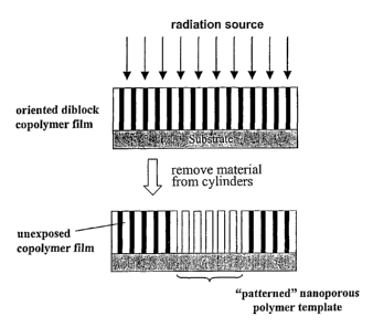
The technique described above is generally depicted in Fig. 1, which shows an
oriented dibloclc copolymer film on a substrate. The darl~ areas on the
substrate
represent one of the components of the diblocl~ copolymer, and the adjacent
lighter
areas represent the other component of the diblocl~ copolymer. The upper
surface of
the copolymer film is here shown perfectly flat. This condition can be
preferable for
some applications, although this is not a requirement for the technique
generally.
Those applications which desirably involve the production of substantially
flat film
surfaces can utilize methods which use a further polpner on top of the
copolymer
film. For example, polydimethylsiloxane can be deposited across the surface of
the
copolymer film to produce a substantially flat surface on the copolymer film.
For particular applications, the matrix material is desirably removed from the
substrate surface after deposition of functional material. In other
applications, the
matrix material is desirably present subsequent to deposition to provide
stnictmal
stability to the array of nanowires, or to allow further post-fabrication
lithographic
steps. Removal of matrix material can be achieved by treating the array with
an agent
that selectively degrades the matrix material with respect to the nanowires as
described above.
Selective Exposure
The methods of certain embodiments described herein are based on the
selective exposure of the diblocl~ copolymer template to a radiation source
which
CA 02451882 2003-09-15
WO 02/073699 PCT/US02/07769
removes material fiom the polymer film, to create three-dimensional nanoscale
elements in a multilevel integrative technology. Special multilevel processing
steps,
specifically tailored to each particular device configuration, are used to
achieve the
complex integration. A simple product may require patterned dibhock level of
lithography only, while a complex integrated product may also require pre- and
post-
fabrication lithographic steps. The common technique to all cases of
nanostructure
fabrication is the selective copolymer patterning technique.
The process involves the selective alteration of specific areas or location of
a
nanoporous copolymer template, e.g., by exposure to a radiation source.
Suitable
radiation sources for the selective degradation of a copolymer component
include, for
example, ultraviolet (W) light, electron beams, or other sources of radiation
that can
efficiently degrade a component of a diblochc copolymer. The process is
depicted
generally in Fig. 2a, which shows a side view of a vertically oriented
diblocl~
copolymer film on a surface, with radiation impinging on the copolymer film.
The
radiation removes material from the film to create cylinders, and since the
exposure is
selective, there are areas of the film that contain cylinders, and areas which
do not.
Fig. 2b is an overhead view of the same film, showing explicitly that, in this
case, a
triangular shape has been imposed on the film surface, resulting in an area
where
electrodeposition can potentially be can-ied out, depending on the
characteristics of
the underlying surface. Fig. 3 depicts the same process and resulting
template, with
the matrix component of the film deleted in Fig. 3 for clarity.
For applications involving the use of UV light, a W mask or UV projection
can be used for spatial selectivity across the surface of the aiTay. For
applications
involving electron beams, a focused electron beam writer or other electron
beam
sowce can be used for spatial selectivity. The exposure pattern imposed on the
surface can be related to, or dictated by, underlying feat-~.ues in the film
or on an
underlying surface, or can be unrelated to such feaW res. For example, when
the
underlying surface includes an electrode patteun, specific ahigmnent of
portions of the
diblocl~ exposure pattern with portions of the electrode pattern can be a
requirement
for device manufacture. The resulting array is referred to as being laterally
patterned.
21
CA 02451882 2003-09-15
WO 02/073699 PCT/US02/07769
Once a patterned nanoporous array template is created, surface-selective
materials deposition methods can be used to locate desired materials into the
pores to
create nanoscale elements. Nanowires will be present only in areas which are
the
union of areas exposed to radiation, and areas containing an electrode
underlying the
surface of the copolymer film.
Novel use of electrochemical deposition methods, for example, enables
several applications. Other surface-selective materials deposition
tec1111iques can be
used, including chemical vapor deposition, electroless deposition, surface
chemistry,
chemical adsorption, and chemically driven layer-by-layer deposition, for
example.
In the case of electrochemical deposition, different electrodes can be held at
differing
voltages during the electrochemical deposition to allow or prevent deposition
at
chosen electrodes, and this technique can be referred to as "programmed
deposition."
Specifically, since the underlying electrodes are separately addressable, one
electrode
(or group of electrodes) can be held at a potential appropriate for deposition
of one
material, while other electrodes are held at potentials which do not allow
depositions
of that material. This method offers expanded materials versatility, in that
different
types of nanowires can be deposited on the salve chip.
An example of this type of nanofabrication is depicted in Fig. 4, which is a
schematic diagram of a multilevel structure created using tile concepts
described
above. In Fig. 4, the matrix component of the copolymer is deleted from view
for
clarity. The substrate includes thlll film electrodes in, or on, its surface,
which can be
created by conventional lithography, for example. Lateral patterning can be
carried
out in registry with the underlying electrode pattern as desired, followed by
elechodeposition of a first material, results in the creation of first
nanowires, as
ShOWIl. Subsequent electrodeposition of a second material, at an electrode
potential
different from that used for the electrodeposition of the first material
results in the
creation of second nanowires, as shown. First and second materials can differ
in
characteristics, particularly in characteristics which are relevant to the
functional
aspects of the devices. The first and second materials can be metals or semi-
metals,
so that characteristics, such as reduction potential, semi-metal type (for
example, "n"-
22
CA 02451882 2003-09-15
WO 02/073699 PCT/US02/07769
or "p"-type semi-metal, metalloid or semiconducting materials), reduction
potential,
and other useful characteristics can be varied in different locations of the
film.
Alternatively, lateral patterning, followed by electrodeposition of a first
material creates first nanowires as shown. Another lateral patterning step, in
a
different location, followed by electrodeposition of a second material, at any
electrode
potential, results in the creation of second nanowires. Subsequent
lithography, also
lmown as electrodeposited post-level connections, on the surface of the film
creates
colmections between sets of nanowires, and allows the creation of simple or
complex
circuits. Fig. 5 shows an overhead view of another example of such a tluee
dimensional structure, emphasizing the relationship between electrical
colmectlons
underlying (level #1), through (level #2), and overlying (level #3) the matrix
component of the dibloclc copolymer to create electrical colmections in
registry with
components on these differing levels.'
In solve applications, it is desirable to use subsequent upper levels of
lithography for intercolmection and integration purposes. Such embodiments are
depicted in Figs. 13a, and 13b, which show two basic configlxrations of
magneto
electronic transport nanodevices. Figs. 13a and 13b depict magneto-electronic
device
configurations that utilize transport current through the nanowires. These
devices
utilize anisotropic magnetoresistance, giant magnetoresistance, or spin-
polarized
current switching magnetoresistance, as discussed in I~atine et al., "Current-
driven
magnetization reversal and spin-wave excitations in Co/Cu/Co pillars," Playr.
Rev.
Lett., 84, (2000), 3149, for magnetic sensing and "spintronic" purposes. They
are
relevant to magnetic data storage read head technology, magnetic RAM, and
magnetic
sensing applications. Fig. 13a shows a first configuration, in which the
"current in"
and "current out" electrodes are on the substrate level, and the
intercolmection
between these two electrodes is on the upper intercomiect level. Fig. 13b
shows a
second configuration, in which the "current in" electrode is on the substrate
Ieve1 and
the "current out" electrode is on the upper intercolmect level. Particular
combinations
of these configurations will be readily apparent to those designing circuits.
A device of the constl-uction depicted in Fig. 13 has been made, and a
microscope photograph of this device is shown in Fig. 17. The patterned blacl~
23
CA 02451882 2003-09-15
WO 02/073699 PCT/US02/07769
regions are the locations of the nanowires. Magnetoresistance measurements of
electron transport through the device depicted in Fig. 17 have been carried
out, and
are shown in Fig. 18.
W addition, the nanowires themselves can be multilayered, using pulsed
electrodeposition in a two-component bath, for example, to create CuCo
multilayers,
or by sequential electrodeposition. Some embodiments of multilayered nanowires
are
depicted in Fig. 13c. Magnetic nanowires are, as discussed above created using
magnetic materials, principally including cobalt, nicl~el, iron, and alloys
containing
these metals, and are useful for anisotropic magnetoresistance applications.
Multilayered magiletic nanowires are created using substantially regularly
alternating
layers of magnetic materials and non-magnetic materials within individual
nanowires
(for example, Co/Cu alternating layers), and are useful for giant
magnetoresistance
applications. Asmmetric mag~letic heterostnictures are made using
substantially
110111egLllarly alternating layers of magnetic and non-magnetic materials,
useful for
spin-polarized current switching magnetoresistance.
Immediately after the selective area exposure, the polymer film contains
polymer in three distinct states: 1) the degradation by-products; 2) the
insoluble
component; and 3) the virgin, oriented diblocl~ copolymer in the unexposed
regions.
The coexistence of these tluee states offers additional fabrication
versatility. By
choice of solvent or radiation, one can choose to remove only the exposed
cylinders,
or alternatively, the exposed cylinders and the unexposed regions of dibloclc
copolymer. For example, acetic acid can be used to remove degraded polymer
fragments from the exposed area, but will not affect the matrix component. An
agent
such as acetic acid will also not remove material from the virgin, wexposed
diblocl~
copolymer. If desired, the removal of material from virgin regions can be
achieved by
treatment with another agent, for example, toluene. If desired, the removal of
the
unexposed diblocl~ copolymer can be chosen to occL~r at a separate stage of
processing, for example, after nanowires have been fabricated in the pores.
It is also relevant to note that for high-dosage over-exposures, both polymer
blocl~s will crosslin~, rendering a solid insoluble film that can also be used
for
fabrication purposes. hl such embodiments, neither component of the diblocl~
24
CA 02451882 2003-09-15
WO 02/073699 PCT/US02/07769
copolymer can be removed. Such areas can be used as robust barners, which
protect
the underlying substrate from further solvent processing. The use of different
combinations of exposure and solvent protocols greatly advance tile general
utility of
the general procedures described herein for the fabrication of nanostnlctures.
In data storage applications, patterning of magnetic arrays can be used to
create patterned perpendicular magnetic media, as shown in Fig. 14a. Each set
of
nanowires is separated from other sets of nanowires by unexposed diblocl~
copolymer.
All individual nanowires within a given set of nanowires have the same
magnetization
direction, either up or down, corresponding to a data bit of either "1" or
''0."
In other applications in which the magnetic switching behavior of magnetic
arrays can be exploited, the laterally patterned arrays described herein are
of utility.
The magnetization switching field of a magnetic nanowire can be modified
substantially by the magnetic Bipolar interactions it experiences due to
neighboring
nanowires, and consequently depends on whether the nanowire is found in a
circle,
triangle, cross- or star-shape, or other shape which tends to maximize or
minimize the
exposure of nanowires to each other or non-magnetic areas of the film. The
lateral
extent and shape of an array of magnetic nanowires will 111f111e11Ce 1tS
SWltChlllg
behavior dramatically. This can be observed in the magnetic hysteresis curve
(magnetization versus applied field) and in the magnetoresistance of a device
using
such wires. Using the patterned dibloclc templates we can create "designer
micromagnetic media." Tlus designer media can be used in magneto-transport
device
technologies that require discontinuous changes at specific threshold fields
or for
other applications that utilize step-wise changes in magnetic field. Some of
Sllch
embodiments are exemplified in Fig. 14b, which show both triangular and
circular
sets of nanowires. The discontinuous switching behavior of designed devices
can be
e1W arced for particular applications.
Auplications
The three dimensional nanostrllctured arrays described herein can be used in
of technologies, including: display technology, cooling technology, magneto-
electTOnic technology, data storage technology, sensor technology,
biomolecular array
CA 02451882 2003-09-15
WO 02/073699 PCT/US02/07769
technology, molecular electronic technology, waveguide technology, and other
technologies. The techniques presented here are general and provide advances
to a
variety of research materials systems.
Field Emission A~~lications
Field emission displays (FEDs) offer high brighW ess, low power
consumption, and flat-panel design. The displays can include an addressable
aiTay of
field emitters and a phosphorescent screen. Efficient field emission displays
require
high-aspect-ratio nanoscale metal tips (for example, from about 20:1, or about
35:1,
or about 50:1 to about 10,000:1) to enable electronic field emission at low
tlueshold
voltages. To achieve a sufficiently large current density, the emitters are
desirably
arranged into a high-density array. To define display pixels, the array is
desirably
patterned laterally into sets of nanowires, with each pixel electronically
addressable.
These sets can include from one to 10, 20, 30, or more nanowires, depending on
the
desired application.
The present invention offers simplified processing and the ability to male tip
arrays with improved orientation.
The ultra-high density, laterally patterned aiTays created by the methods
described herein can be successfully used for high-resolution, low power, thin
and
flexible display devices. The high aspect ratio of nanowires created by the
techniques
described herein allow the threshold voltage for emission to be sufficiently
low so that
power consumption for such field emission devices is correspondingly lowered.
The
devices are useful for television and video screens, computer monitor screen,
and
many other display devices such as on watches, GPS devices, and any other
devices
currently using LED or LCD displays . The thinness of such field emission
aiTays
allows the design of such devices to be far thimler than devices available
currently.
Display devices made with the technology described herein are also much
brighter for
a given level of energy consumption than those cmTenthy available. The
possibility of
using a flexible substrate further expands the utility of display devices made
with the
techniques described herein. Differing display applications will have
differing
26
CA 02451882 2003-09-15
WO 02/073699 PCT/US02/07769
priorities as regards operating characteristics; for example, an outdoor
display caxl
require high brightness, and a video display can require lugh resolution.
An example of a field emission array created according to the methods
described herein is shown in Fig. 6, which is a perspective view of a diagram
of such
an array. The substrate has electrodes in or on its surface, created by
conventional
lithography. Diblocl~ copolymer is deposited on the substrate, as described
above, for
example, by spin-bonding. Vertical orientation, selective irradiation,
chemical
treatment, and electrodeposition follow to create sets of nanowires, in this
case,
deposited on two distinct electrodes. For field emission applications, the
ends of the
nanowires are desirably at or near the film surface. This can be achieved by
either
growing (that is, electrodepositing) the wires to substantially the full film
thiclmess, or
by growing them to a lesser extent (for example, 90% of the film thiclmess),
followed
by removal of a portion of the surface of the film, by means l~nown to those
of skill in
the aut (including, for example, reactive ion etching by oxygen plasma).
Again, the
matrix component is deleted from Fig. 6 for clarity.
A device according to the constriction of Fig. 6 was made, and microscope
photographs of this device are shovnnn in Fig. 19. The dibloclc template is
shown
patterned into a circular region at 20x magnification in the upper left of
Fig. 19. The
same region is shown after 250 mn cobalt nanowires have been grovcm at-1V into
the
circular region, but before electrical measurements were made at 20x
mag~lification in
the upper right of Fig. 19. The same region is shown after electrical
measurements
were made and then having brought up the emission current to the point at
which the
sample was destroyed in the lower part of Fig. 19 (lower left at Sx
magnification,
lower right at 20x magnification). Fig. 20 shows a graph of electronic field
emission
measurements made from the array shown in Fig. 19. A large current density and
a
low threshold was achieved. Fig. 21 is a close up of the images from Fig. 19,
upper
right and lower left, before and after destroying the sample, respectively.
The electrodes are individually addressable, in this .case, with voltages V ~
and
V2. These applied voltages are independently varied as desired to control
(that is, tum
"on" and "off') the emission cu3Tent from each nanowire set. A phosphor screen
can
be placed above the nanowire sets to create a display. Fig. 7 shows an
overhead view
27
CA 02451882 2003-09-15
WO 02/073699 PCT/US02/07769
of a similar device, but with four individually addressable sets of nanowires.
It is
important to note that nanowires are deposited only on the substrate where: 1)
the
copolymer is exposed to irradiation that degrades a component of the copolymer
down to the substrate surface; 2) the residue of degraded component is removed
from
the substrate surface; and 3) the substrate surface has an electrical contact
allowing
electrodeposition.
Thermoelectric CooliyApplications
Solid-state cooling devices can also be designed utilizing the tecln~ology
described herein. At present, the best commercially available thermoelectric
cooling
devices have thernoelectric figimes of merit of approximately 0.1. The
techniques
described herein can produce devices which have thermoelectric figimes of
merit
approaching or exceeding 2.0, e.g., devices having a figure of unit of 0.5,
0.7, 0.9, 1.0,
1.2, 1.5, 1.7, 1.8, 1.11, 2.0 or greater.
Fig. 9 is a diagram of a single-stage thermoelectric cooler which can be made
according to the methods described herein. The substrate has electrodes pre-
patterned
in or on its surface. A patterned diblocl~ copolymer layer is created on the
substrate,
as described herein. Again, the matrix component of the copolymer is deleted
in Fig.
9 for clarity. Nanowires of two types are deposited by programmed
electrodeposition.
In the depicted example, "n-type" nanowires, made from ''n-type" materials,
well
la~own in the ant, are deposited at one electrode, and "p-type" nanowires,
made from
"p-type" materials, also well lmovv~m in the art, are deposited at another
electrode. A
top-layer metal interconnect is then deposited electrochemically. The device
operates
through the application of current through the device, so that the top plate
becomes
cold and the electrodes and substrate become warn. The top plate can be used
as a
heat sinlc for use in electronic devices, for example. Multistage coolers can
also be
made by this fabrication method. Heating devices are also made possible by the
simple adaptation of the device for such proposes.
28
CA 02451882 2003-09-15
WO 02/073699 PCT/US02/07769
Magnetic Data Storage Applications
Next generation magnetic data storage technologies will likely utilize
perpendicular magnetic media to store data. Present technologies use lateral
magnetic
media in which the magnetic storage elements lie along the surface of the
substrate.
W the effort of packing more elements per unit area, the size of the basic
elements
must be reduced. This introduces a problem, however, since as the scale of
these
regions is reduced, so is the bloclcing temperature which marks the onset of
superparamagnetism. The blocking temperature must be kept large, otherwise the
stored magnetization state of each element will decay and data will be lost.
One way to reduce the size scale of a magnetic media element without
substantially reducing the blocking temperature is to utilize shape and
volume, that is,
to make small cylindrically-shaped objects of high aspect ratio (for example,
from
about 20:1, or about 35:1 or about 50:1 to about 10,000:1). All other
considerations
being equal, a cylindrically-shaped magnet of diameter 10 nm and length of 500
nm
will have a much higher blocking temperature than that of a spherical magnet
of 10
nna diameter. The highest spatial packing density of magnetic cylinders occurs
for
cylinders in a vertical hexagonal closed-packed arrangement.
W the bulk, pure cobalt is a soft ferromagnet of relatively low coercivity and
not necessarily an ideal material for magnetic data storage. However, certain
cobalt
alloys have "designer" magnetic properties including engineered coercivity
which
malces them useful for present-day magnetic media applications. These cobalt
alloys
can be electro-deposited from a specific plating bath containing the relevant
ions.
The techniques described herein can be used to create arrays useful for the
next generation of magnetic data storage. Since the surface smoothness of such
arrays
can be important, it is considered desirable to utilize an auxiliary pol5nner
to produce
highly smooth films on substrate surfaces. Highly smooth films can be created
by
depositing polydimethylsiloxane on a diblock copolymer film, as described in
copending United States Patent Application Serial No. 09/814,891, filed March
22,
2001, titled "Nanocylinder Arrays." The application is incorporated herein by
reference in its entirety.
29
CA 02451882 2003-09-15
WO 02/073699 PCT/US02/07769
Engineered MaQ;netoresistance Applications
Magneto-electronic devices can be used for magnetic sensing applications
(e.g., magnetic data storage) and for "spintronics" (e.g.,.MRAM).
Appropriately
chosen nanoscale magnetic architectures can result in improved perfomnance
since
magnetic interactions can be tuned at the manometer scale. The techniques
described
herein can be used to create devices in a variety of useful magneto-electronic
configurations.
Materials have been developed over the last ten years that are now used for
magnetic sensing by utilizing their giant magnetoresistive (GMR) properties.
These
materials have various architectures, but in general are muhtilayered
materials with
layers of non-magnetic metals in contact with layers of magnetic metals. The
magnetic interlayer-exchange-coupling and electron spin-dependent scattering
leadJto
the sensitivity of resistance with respect to magnetic field. Tuning the
stricture of
these systems by materials engineering allows mag~letoresistive properties to
be
optimized for applications. GMR read heads in hard-dislc drive teclmology is
one
important commercial application. These engineered materials systems are
expected
to advance with better materials and new material architectures.
The magnetic arrays made using techniques described herein show GMR type
behavior. However, the architecture of these arrays is significantly different
than
others that have been produced. The important consideration for GMR device
design
is that there be electrical contact between the substrate and the
magnetic~nanowires,
not whether the wires are embedded in the template or not. Therefore, the
wires can
be grown (that is, electrodeposited) to less than the film thichmess for GMR
devices
without a need to remove matrix material prior to operability.
Of l~ey importance to optimal performance of GMR devices is the ability to
form a regular array of very small dimensions, for example, an aiTay of 25.4
manometer period made of cylinders 11 manometers in diameter. Furthermore the
fabrication processes described herein permit the well-controlled height of
the
cylinders, and the ability to muhtilayer the cylinder material as it is grown.
These new
processing considerations have allowed the creation of new geometrical
archutectures
at size scales that have not been achieved using h~nown fabrication processes.
By
CA 02451882 2003-09-15
WO 02/073699 PCT/US02/07769
tuning material structure in the fabrication processes described herein, a new
breed of
GMR materials is possible.
A particular embodiment of a GMR device is shown in Fig. 10. The device is
created by fabricating a magnetic nanoarray as described herein on a substrate
patterned with an electrode. This particular magnetoresistive device is in a
"lateral
transport" configuration (the transport current is affected by the presence of
the
magnetic nanowires, but is not configured to pass through the wire along its
length).
Again, the matrix component of the copolymer is deleted fiom Fig. 10 for
clarity.
The nanowires for such a device are desirably asyzrnnetric magnetic
heterostnuctures,
as described above with respect to Fig. 13c. Fig. 13c does not imply that in a
given
set of nanowires, all three types are used, rather that any one of the types
can be
employed in a set.
Smart Media Applications
"Smaz-t media" are media that sense this enviromnent in a particular way, and
create a measurable response. This could be, for example, a chemical sensor in
which
the device produces an electrical current when the presence of a particular
type of
molecule in solution is detected. Any electrical version of patterned smart
media
could be integrated with other signal processing on the same chip. Another
example
is a sensing medizun that changes color upon sensing a change in chemical
environment, temperature environment, optical stimulus, or other type of
stimulus.
Since the diblocl~ systems are laterally patterned, arrays with large munbers
of distinct
sensing elements are fabricated. Each element is a localized transducer that
is
integrated into an on-chip circuit.
Presently, the techniques described herein can be used to produce nanowire
az~ays with a nanoelement density of approximately 1.2 x 10¹² elements/in2.
This
ultimately enables data storage technologies with storage capacities exceeding
a
terabit/in2. Patterned versions of high-density media in which one bit of data
is
encoded in the magnetization of a group of magnetic nanowires are created. The
pattez-ned diblocl~-derived devices described herein provide a simple
fabrication route
to lugh storage densities.
31
CA 02451882 2003-09-15
WO 02/073699 PCT/US02/07769
Electrochemical Sensor Applications
These sensors are used in a wide range of applications, including portable
glucose detection for people with diabetes. The nanoporous templates disclosed
herein are used conveniently to malce devices for electrochemical sensing as
an array
of "microelectrodes." In the electrochemistry literature the term
"microelectrode"
refers to a conf guration of electrode that induces oadial diffusion of an
electrochemically-active species toward the electrode. The behavior of a
microelectrode differs dramatically from that of a planar electrode. A
nanoporous
polyner template nanoelectrode array as described herein offers fast response,
lower
detection limits, and the possibility for molecular selectivity based on size
or
molecular interactions with the template. The lateral-patterning invention
advances
the use of nanoporous templates for this purpose because several distinct
microelectrodes arrays are configured onto the same chip using patterned
diblocl~
templates atop a pre-patterned thin-film electrode set.
Biomolecule ArrayApplications
Combinatorial chips are configured for DNA gene expression studies and
other diagnostic applications. The nanoporous polymer templates described
herein
are patterned and filled with metals or silicon oxide that are used to attach
biomolecules that will enable new types of biomolecular research capabilities.
Patterned versions of such structures are of far greater usefulness. Another
application for lateral patterning is to create structures for sorting
molecules in
nanoscales.
Molecular Electronics Applications
Specific types of molecules and small colloidal clusters are used as electroW
c
devices. The goal is to "design in" electronic functionality (e.g.,
rectification,
switclung, negative differential resistance) by synthesizing molecules using
certain
types of end groups, aromatic rings and side groups. Interfacing these
molecules for
electrical characterization using lmown techniques is extremely challenging.
32
CA 02451882 2003-09-15
WO 02/073699 PCT/US02/07769
However, new patterned nanoporous templates can be used as a practical host
substrate for the characterization of specific types of electroncally relevant
molecules. The diblocl~ template is patterned in regions atop pre-patterned
gold
electrodes. The molecules axe adsorbed to the gold at the bottom.of each pore
using a
thiol-gold interaction. This results in a self assembled monolayer of the
electronic
molecules at the bottom of each pore. A counter electrode is deposited
electrochemically atop the molecular layer and contacted using the patterned
interconnections described above. This fabrication scheme enables convenient
electrical characterization of candidate molecules.
Photonic-bandgap Structure Applications
A photonic-bandgap crystal is a optical material that has periodically
modulating dielectric constant. As a consequence of the periodic stnictme, the
transmission properties become dependent on the incident light frequency such
that
certain frequencies, there is no transmission (the dispersion relation ~ (h)
is non-linear
and has derivative of zero at Brillouin zone boundaries, l~ _ ~/a, where a is
the crystal
lattice period). Using these materials, a range of devices can be configured
in analogy
to electronic devices. Once dibloclc copolymer systems can be made with a
sufficiently long-range array order, they can be patterned in specific shapes
to
fabricate planar photonic-crystal waveguides and other photonic-crystal
devices.
Photonic waveguides are able to have much smaller twn radius as compared to
optical
fiber. Such waveguides can be used to intercormect on-chip optical components.
Electrical hltercomlections to Nanowires
Electrical interconnections can be made to nanowires made by patterned
diblocl~ copolymer templates. This is achieved by integrating the templating
process
with other pre- and post-processing steps.
Am important step in utilizing electrical nanostmctures is malting appropriate
electrical interfaces to these nanostructures. hl Figure 15, one embodiment of
the
present invention is realized. First, electrodes are prepattemed onto the
substrate by a
33
CA 02451882 2003-09-15
WO 02/073699 PCT/US02/07769
suitable lithographic technique. Secondly, a diblocl~ copolymer film is
deposited.
Next, a metal layer is deposited. Finally, a conventional (photo- or e-beam-)
resist is
deposited. The cylinders of the diblocl~ copolymer can be oriented by the
techniques
described herein. The resulting structure is shown in Fig. 15a.
Selected areas of the top resist are exposed lithographically and removed by
chemical development. Subsequently the exposed metal layer (#2) is removed by
a
metal etch. At tlus point the diblocl~ filin is exposed to ultraviolet (LTV)
light or an
electronic beam, if it has not been exposed in a prior step. ThIS St111CtL1Te
1S ShOWll 111
Fig. 15b.
The diblocl~ film is now chemically developed with acetic acid or another
suitable developer to result in a nanoporous template. If desired, the surface
of the
nanoporous template can be cleaned using a reactive ion etch with oxygen. This
structure is shown in Fig. 15c.
Nanowires or other suitable nanostructures are now deposited into the pores of
the nanoporous template. To achieve top electrical contact, the deposition can
continue until electrical connection is made with the top layer. As discussed
herein, a
range of different desired nanostructures~ can be deposited in the pores,
depending on
the target application. This structure is shown in Fig. 15d.
In some applications, such as field emissions arrays, electrical contact to
the
top layer is not desired. Rather, the isolated top metal layer would be used
as an
electrical gate in a triode field emission device configuration. In other
applications,
metal contact #2 can be replaced over the deposited nanowires to complete
contact
t1>1 ough the wires, as shown in Fig. 15 e.
The integration scheme described in Figure 15 represents only one out of
several schemes for integration and interfacing nanostllictures made by
patterned
nanoporous templates. Nanofabrication via patterned diblocl~ copolymers can be
combined easily with other (pre- and post-) process steps, and done so such
that the
pattern is made in registry with previous lithographic pattelms.
Another fabrication scheme can be described as follows. First, electrodes are
prepatterned onto the substrate by a suitable lithographic technique.
Secondly, a
34
CA 02451882 2003-09-15
WO 02/073699 PCT/US02/07769
diblocl~ copolymer film is deposited. The diblocl~ cyclinders are then
oriented ,
exposed lithographically in a desired pattern, and then developed into a
nanoporous
template. Nanowires or other suitable nanostructures are now deposited into
the pores
of the nanoporous template.
, To achieve top electrical contact, or top non-contact electrodes, a suitable
lithographic exposure and development, a ion etch performed to remove degraded
portions (for example, oxide) from the top of the nanowires, and then
deposition of
metal electrodes in the contact areas.
The following examples do not limit the scope of the invention described in
the claims.
EXAMPLES
The following examples illustrate particular properties and advantages of
some of the embodiments.
Example 1: A Prototype of a Field Emission Array
Figs. 8a-8d are 10X optical images of a prototype of a field emission array
built by the inventors. In Fig. 8a, the silicon substrate was gold patterned
with
conventional lithography with a 1 micrometer thicl~, vertically oriented
dibloclc
copolymer film (polystyrene/pol5nnethylmethacrylate, 70/30 by volume) covering
the
entire surface (the film is optically transparent). Fig. 8b is an image of the
same
sample after electron-beam patterning in the shape of a square, and acetic
acid
development. The inner square was a patterned nanoporous template. The outer
square was a solid film of crosslinl~ed polystyrene/polylnethyhnethacrylate
made by
intentional overexposure to radiation. Fig. 8c is an ianage of the same sample
after
500 mn length cobalt wires were electrodeposited in the template. The cobalt
is blacl~
in the image. Fig. 8d is a close-up of the electrodeposited area. It is
important to note
that the nanowires deposit only in the nanoporous template regions with metal
underneath.
35
CA 02451882 2003-09-15
WO 02/073699 PCT/US02/07769
Example 2: A Prototype Ma~netorasistive Device
Figs. l la and l 1b are lOX optical images of a prototypical four-wire
magnetoresistive device made by the inventors. An array of vertical magnetic
nanowires stands atop a thin-film of gold pre-patterned into a four-probe
resistor
pattern. This device is used to investigate spin-dependent scattering in a
"current-in-
plane" (CIP) geometry where the scattering interface is geometrically periodic
on the
scale of tens of manometers. Fig. 1 la is an image of a substrate with a
patterned
electrode underlayer covered with an optically transparent dibloclc copolymer
film
layer prepared as described in Example 1.
The four probe resistor pattern was created as 2 X1,111 111 Wldth alld 1 OO
~,L111 111
length, by standard electron beam lithography using a PMMA resist on a silicon
substrate. The thin-film resistor includes a 20 nm thicl~ gold layer on top of
a 1 lnn Cr
adhesion layer. A 1.1 ~,m thicl~ film of poly(styrene-(3-methylmethacrylate)
diblocl~
copolymer denoted P(S-(3-MMA) having 30% by volume polylnethylmethacrylate
(PMMA) with molecular weight of 42,000 Daltons was spun coated onto the
patterned surface of substrate. This copolymer microphase separates into a
hexagonal
array of PMMA cylinders in a polystyrene (PS) matrix. Almealing thin films at
180°C, above the glass transition temperature under an applied electric
field, orients
the PMMA cylinders rionnal to the fihn surface, enabling the fabrication of
nanostructures with large aspect ratios. The sample was then exposed to an
electron
beam impinging on the sample in the shape of a square (area dose of 50
~,C/cmz, with
beam energy and current used is 20 l~V and 2000 pA, respectively. Generally,
for
such dibloclc films of about 1 micron, the exposure dose can range from about
20 to
about 200 ~.C/cm2, with accelerating voltages and beam currents as described
above.
Optimal doses have been found to be about 80 ~,C/cln2. The sample was then
chemically developed with acetic acid. The original copolymer remains in the
unexposed areas.
Cobalt nanowires were deposited in the pores on top of the gold pattern from
an aqueous deposition bath, prepared by mixing 96 grams of CoS04~7Hz0 and 13.5
grams H3B03 in 300 ml pure HZO, with 60 ml of methanol added as surfactant,
resulting in an electrolyte pH of 3.7. The Co was electroplated at a reduction
potential
36
CA 02451882 2003-09-15
WO 02/073699 PCT/US02/07769
of -1.OV with respect to a saturated calomel reference electrode. The
nanowires were
500 nm in length. Fig. l 1b is an image of the same sample after nanowire
electrodeposition.
Structural information was obtained by performing small angle X-ray
scattering (SAXS) and field emission scanning electron microscopy (FESEM). The
SAXS data confirms a perpendicular nanowire orientation with a period of 21.7
mn.
The sample was cleaved in two, and FESEM used to examine a cross-section of
the
nanowire array. The diameter of the nanowires was found to be approximately 11
mn,
with a period of 21.8 lnn. At this scale, the individual magnetic naazowires
should be
single-domain in equilibrium, and show interesting magnetoresistance (MR)
effects,
since the interwire spacing is less than the spin diffusion length.
Example 3: Giant Ma~letoresistance Device and Measurements
The four-wire magnetoresistive device prepared in Example 2 was used for
1S measurement. The magnetic cobalt nanowire array is composed of 14 mn
diameter
wires, each 500 lnn long, arranged in a hexagonal lattice With a period of 24
mn. The
structure of the device was verified by shall-angle X-ray scattering
measurements.
The magnetic field direction is parallel to the nanowire axis. A cross
sectional
scamling electron micrograph (SEM) image of such an array is shown in Fig.
12b.
The GMR ratio as a fimction of temperature between 2I~ and 300I~ 1S ShOWTI 111
Fig.
12a. The data tal~en at 2K shows the largest amplitude curve, and that taken
at 300K
shows the smallest amplitude curve, with intermediate temperatures having
intermediate values, with amplitudes in line with the ordering of the
temperature.
Other GMR ratios, as a function of orientation of magnetic field and
temperature are shown in Figs. 16a-c. The magnetoresistance is defined as
[R(H) -
R(501~0e)/R(50 lcOe)]. Again, the data taken at 2I~ shows the largest
amplitude
curve, and that tal~en at 300K shows the smallest amplitude curve, with
intermediate
temperatures having intermediate values, with amplitudes in line with the
ordering of
the temperature. In the "perpendicular" orientation '(fig. 16a), the field is
normal to
the plane of the Au film (parallel to the Co nanowires) and the current
direction. For
the "transverse" orientation (Fig. 16b) and "longitudinal" orientation (Fig.
16c), the
37
CA 02451882 2003-09-15
WO 02/073699 PCT/US02/07769
field is in the plane of the gold film (perpendicular to the Co wires), but
perpendicular
or parallel to the current direction, respectively. The, different shapes and
values for
the MR curves for the three orientations provide evidence for the coexistence
of
anisotropic magnetoresistance (AMR) and giant magnetoresistance (GMR)
scattering
mechanisms in this system.
MR behavior of the Co nanowires was also investigated as a ft111Ct~o11 Of gold
film thiclcness and Co nanowire length. Gold films of 7.5, 10 and 20 inn
thiclmess
were studied with Co nanowires of 500 nm. Also, samples of Co nanowire lengths
of
100 and 500 nm were prepared having gold film thiclmess of 20 inn. MR behavior
was found to depend principally on nanowire length. A plot of normalized
MR",aX for
a perpendicular orientation at 0 field versus temperature for various gold
filin
thiclcn.esses and Co nanowire lengths is shown in Fig. 22. The characteristics
clearly
indicate that the temperature dependence of MR is strongly dependent on the Co
nanowire length, but not so strongly on the gold film thiclmess. Each data set
is
I S normalized to its 2K value for comparison.
OTHER EMBODIMENTS
It is to be understood that while the invention has been described in
conjwction with the detailed description thereof, that the foregoing
description is
intended to illustrate and not limit the scope of the invention, which is
defined by the
scope of the appended claims. Other aspects, advantages, and modifications are
within the scope of the following claims.
38