Note: Descriptions are shown in the official language in which they were submitted.
CA 02451931 2008-02-15
PHASE CHANGE INK IMAGING COMPONENT
WITH NANO-SIZE FILLER
BACKGROUND OF THE INVENTION
The present invention relates generally to an imaging apparatus
and layers for components thereof, and for use in offset printing or ink jet
printing apparatuses. The layers herein are useful for many purposes
including layers for transfer components, including transfix or transfuse
components, imaging components, and like components. More
specifically, the present invention relates to layers comprising nano-size
fillers. The layers of the present invention may be useful in components
used in combination with ink, dye or pigment-based materials. In
embodiments, the layers can be used in combination with phase change
inks such as solid inks, gel-based inks, ultraviolet curable inks, and other
phase-change inks.
Ink jet printing systems using intermediate transfer, transfix or
transfuse members are well known, such as that described in U.S. Patent
4,538,156. Generally, the printing or imaging member is employed in
combination with a printhead. A final receiving surface or print medium is
brought into contact with the imaging surface after the image has been
placed thereon by the nozzles of the printhead. The image is then
transferred and fixed to a final receiving surface.
More specifically, the phase-change ink imaging process begins by
first applying a thin liquid, such as, for example, silicone oil, to an
imaging
member surface. The solid or hot melt ink is placed into a heated reservoir
where it is maintained in a liquid state. This highly engineered ink is
formulated to meet a number of constraints, including low viscosity at
jetting temperatures, specific visco-elastic properties at component-to-
media transfer temperatures, and high durability at room temperatures.
Once within the printhead, the liquid ink flows through manifolds to be
ejected from microscopic orifices through use of proprietary piezoelectric
transducer (PZT) printhead technology. The duration and amplitude of the
-1-
CA 02451931 2008-02-15
electrical pulse applied to the PZT is very accurately controlled so that a
repeatable and precise pressure pulse can be applied to the ink, resulting
in the proper volume, velocity and trajectory of the droplet. Several rows
of jets, for example four rows, can be used, each one with a different
color. The individual droplets of ink are jetted onto the liquid layer on the
imaging member. The imaging member and liquid layer are held at a
specified temperature such that the ink hardens to a ductile visco-elastic
state.
After depositing the image, a print medium is heated by feeding it
through a preheater and into a nip formed between the imaging member
and a pressure member, either or both of which can also be heated. A
high durometer synthetic pressure member is placed against the imaging
member in order to develop a high-pressure nip. As the imaging member
rotates, the heated print medium is pulled through the nip and is pressed
against the deposited ink image with the help of a pressure member,
thereby transferring the ink to the print medium. The pressure member
compresses the print medium and ink together, spreads the ink droplets,
and fuses the ink droplets to the print medium. Heat from the preheated
print medium heats the ink in the nip, making the ink sufficiently soft and
tacky to adhere to the print medium. When the print medium leaves the
nip, stripper fingers or other like members, peel it from the printer member
and direct it into a media exit path.
To optimize image resolution, the transferred ink drops should
spread out to cover a predetermined area, but not so much that image
resolution is compromised or lost. The ink drops should not melt during
the transfer process. To optimize printed image durability, the ink drops
should be pressed into the paper with sufficient pressure to prevent their
inadvertent removal by abrasion. Finally, image transfer conditions should
be such that nearly all the ink drops are transferred from the imaging
member to the print medium. Therefore, it is desirable that the imaging
member has the ability to transfer the image to the media sufficiently.
The imaging member is multi-functional. First, the ink jet printhead
-2-
CA 02451931 2008-02-15
prints images on the imaging member, and thus, it is an imaging member.
Second, after the images are printed on the imaging member, they can
then transfixed or transfused to a final print medium. Therefore, the
imaging member provides a transfix or transfuse function, in addition to an
imaging function.
In order to ensure proper transfer and fusing of the ink off the
imaging member to the print medium, certain nip temperature, pressure
and compliance are required. Unlike laser printer imaging technology in
which solid fills are produced by sheets of toner, the solid ink is placed on
the imaging member one pixel at a time and the individual pixels must be
spread out during the transfix process to achieve a uniform solid fill. Also,
the secondary color pixels on the imaging member are physically taller
than the primary color pixels because the secondary pixels are produced
from two primary pixels. Therefore, compliance in the nip is required to
conform around the secondary pixels and to allow the primary pixel
neighbors to touch the media with enough pressure to spread and
transfer. The correct amount of temperature, pressure and compliance is
required to produce acceptable image quality.
Currently, the imaging member useful for solid inks or phase
change inks comprises anodized aluminum. This member operates at
about 57 C to about 64 C and can be used with a heater that preheats the
print media prior to entering the nip. Otherwise, the imaging member may
include a heater associated therewith. The heater may be associated
anywhere on the offset printing apparatus. The current aluminum-imaging
member has several drawbacks. A high nip load of up to about 770
pounds is needed for transfix or transfuse operations. Further, because of
the high nip load, bulky mechanisms and supporting structures are
needed, resulting in increased printer weight and cost. One example is
that a fairly complex two-layer pressure roller is needed. In addition, the
first copy out time is unacceptable because of the bulky weight.
Moreover, low cohesive failure temperature is another drawback to use of
an anodized aluminum drum.
-3-
CA 02451931 2008-02-15
Several coatings for the imaging member have been suggested.
Examples are listed below.
U.S. Patent 5,092,235 discloses a pressure fixing apparatus for ink
jet inks having 1) outer shell of rigid, non-compliant material such as steel,
or polymer such as acetal homopolymer or Nylon 6/6 and 2) an underlayer
of elastomer material having a hardness of about 30 to 60, or about 50 to
60.
U.S. Patent 5,195,430 discloses a pressure fixing apparatus for ink
jet inks having 1) outer shell of rigid, non-compliant material such as steel,
or polymer such as acetal homopolymer or Nylon 6/6 and 2) an underlayer
of elastomer material having a hardness of about 30 to 60, or about 50 to
60, which can be polyurethane (VIBRATHANETM, or REN:C:O-thaneTM).
U.S. Patent 5,389,958 discloses an intermediate transfer
member/image receiving member having a surface of metal (aluminum,
nickel, iron phosphate), elastomers (fluoroelastomers,
perfluoroelastomers, silicone rubber, polybutadiene), plastics
(polyphenylene sulfide), thermoplastics (polyethylene, polyamide (nylon),
FEP), thermosets (metals, ceramics), and a pressure roller with elastomer
surface.
U.S. Patent 5,455,604 discloses a fixing mechanism and pressure
wheels, wherein the pressure wheels can be comprised of a steel or
plastic material such as DELRINTM. Image-receiving drum 40 can be a
rigid material such as aluminum or stainless steel with a thin shell
mounted to the shaft, or plastic.
U.S. Patent 5,502,476 teaches a pressure roller having a metallic
core with elastomer coating such as silicones, urethanes, nitriles, or
EPDM, and an intermediate transfer member surface of liquid, which can
be water, fluorinated oils, glycol, surfactants, mineral oil, silicone oil,
functional oils such as mercapto silicone oils or fluorinated silicone oils or
the like, or combinations thereof.
U.S. Patent 5,614,933 discloses an intermediate transfer
member/image receiving member having a surface of metal (aluminum,
-4-
CA 02451931 2008-02-15
nickel, iron phosphate), elastomers (fluoroelastomers,
perfluoroelastomers, silicone rubber, polybutadiene), plastics
(polyphenylene sulfide), thermoplastics (polyethylene, polyamide (nylon),
FEP), thermosets (metals, ceramics), or polyphenylene sulfide loaded with
PTFE, and a pressure roller with elastomer surface.
U.S. Patent 5,790,160 discloses an intermediate transfer
member/image receiving member having a surface of metal (aluminum,
nickel, iron phosphate), elastomers (fluoroelastomers,
perfluoroelastomers, silicone rubber, polybutadiene), plastics
(polyphenylene sulfide), thermoplastics (polyethylene, polyamide (nylon),
FEP), thermosets (metals, ceramics), or polyphenylene sulfide loaded with
PTFE, and a pressure roller with elastomer surface.
U.S. Patent 5,805,191 an intermediate transfer member/image
receiving member having a surface of metal (aluminum, nickel, iron
phosphate), elastomers (fluoroelastomers, perfluoroelastomers, silicone
rubber, polybutadiene), plastics (polyphenylene sulfide), thermoplastics
(polyethylene, polyamide (nylon), FEP), thermosets (metals, ceramics), or
polyphenylene sulfide loaded with PTFE, and an outer liquid layer of
liquid, which can be water, fluorinated oils, glycol, surfactants, mineral
oil,
silicone oil, functional oils such as mercapto silicone oils or fluorinated
silicone oils or the like, or combinations thereof.
U.S. Patent 5,808,645 discloses a transfer roller having a metallic
core with elastomer covering of silicone, urethanes, nitriles, and EPDM.
U.S. Patent 6,196,675 B1 discloses separate image transfer and
fusing stations, wherein the fuser roller coatings can be silicones,
urethanes, nitriles and EPDM.
U.S. Patent 5,777,650 discloses a pressure roller having an
elastomer sleeve, and an outer coating that can be metals, (aluminum,
nickel, iron phosphate), elastomers (fluoroelastomers,
perfluoroelastomers, silicone rubber, polybutadiene), plastics
(polyphenylene sulfide with PTFE filler), thermoplastics (polyethylene,
polyamide (nylon), FEP), thermosets (acetals, ceramics). Preferred is
-5-
CA 02451931 2008-02-15
anodized aluminum.
In addition, many different types of outer coatings for transfer
members, fuser members, and intermediate transfer members have been
used in the electrostatographic arts using powder toner, but not with liquid
inks or phase change inks. Several examples are listed herein.
U.S. Patent 5,361,126 discloses an imaging apparatus including a
transfer member including a heater and pressure-applying roller, wherein
the transfer member includes a fabric substrate and an impurity-absorbent
material as a top layer. The impurity-absorbing material can include a
rubber elastomer material.
U.S. Patent 5,337,129 discloses an intermediate transfer
component comprising a substrate and a ceramer or grafted ceramer
coating comprised of integral, interpenetrating networks of haloelastomer,
silicon oxide, and optionally polyorganosiloxane.
U.S. Patents 5,340,679 discloses an intermediate transfer
component comprised of a substrate and thereover a coating comprised of
a volume grafted elastomer, which is a substantially uniform integral
interpenetrating network of a hybrid composition of a fluoroelastomer and a
polyorganosiloxane.
U.S. Patent 5,480,938 describes a low surface energy material
comprising a volume grafted elastomer which is a substantially uniform
integral interpenetrating network of a hybrid composition of a
fluoroelastomer and a polyorganosiloxane, the volume graft having been
formed by dehydrofluorination of fluoroelastomer by a nucleophilic
dehydrofluorinating agent, followed by a hydrosilation reaction, addition of
a hydrogen functionally terminated polyorganosiloxane and a hydrosilation
reaction catalyst
U.S. Patent 5,366,772 describes a fuser member comprising a
supporting substrate, and a outer layer comprised of an integral
interpenetrating hybrid polymeric network comprised of a haloelastomer, a
coupling agent, a functional polyorganosiloxane and a crosslinking agent.
-6-
CA 02451931 2008-02-15
U.S. Patent 5,456,987 discloses an intermediate transfer
component comprising a substrate and a titamer or grafted titamer coating
comprised of integral, interpenetrating networks of haloelastomer, titanium
dioxide, and optionally polyorganosiloxane.
U.S. Patent 5,848,327 discloses an electrode member positioned
near the donor member used in hybrid scavengeless development,
wherein the electrode members have a composite haloelastomer coating.
U.S. Patent 5,576,818 discloses an intermediate toner transfer
component including: (a) an electrically conductive substrate; (b) a
conformable and electrically resistive layer comprised of a first polymeric
material; and (c) a toner release layer comprised of a second polymeric
material selected from the group consisting of a fluorosilicone and a
substantially uniform integral interpenetrating network of a hybrid
composition of a fluoroelastomer and a polyorganosiloxane, wherein the
resistive layer is disposed between the substrate and the release layer.
U.S. Patent 6,035,780 discloses a process for forming a layer on a
component of an electrostatographic apparatus, including mixing a first
fluoroelastomer and a polymeric siloxane containing free radical reactive
functional groups, and forming a second mixture of the resulting product
with a mixture of a second fluoroelastomer and a second polysiloxane
compound.
U.S. Patent 5,537,194 discloses an intermediate toner transfer
member comprising: (a) a substrate; and (b) an outer layer comprised of a
haloelastomer having pendant hydrocarbon chains covalently bonded to
the backbone of the haloelastomer.
U.S. Patent 5,753,307 discloses fluoroelastomer surfaces and a
method for providing a fluoroelastomer surface on a supporting substrate
which includes dissolving a fluoroelastomer; adding a dehydrofluorinating
agent; adding an amino silane to form a resulting homogeneous
fluoroelastomer solution; and subsequently providing at least one layer of
the homogeneous fluoroelastomer solution to the supporting substrate.
-7-
CA 02451931 2008-02-15
U.S. Patent 5,840,796 describes polymer nanocomposites including
a mica-type layered silicate and a fluoroelastomer, wherein the
nanocomposite has a structure selected from the group consisting of an
exfoliated structure and an intercalated structure.
U.S. Patent 5,846,643 describes a fuser member for use in an
electrostatographic printing machine, wherein the fuser member has at
least one layer of an elastomer composition comprising a silicone
elastomer and a mica-type layered silicate, the silicone elastomer and
mica-type layered silicate form a delaminated nanocomposite with silicone
elastomer inserted among the delaminated layers of the mica-type layered
silicate.
U.S. Patent 5,933,695 discloses a rapid wake up fuser member
comprising a substrate, a heat transmissive layer provided on the substrate
and having a silicone material and a Q-resin, and a toner release layer
comprising a polymer and provided on the heat transmissive layer.
U.S. Patent 4,853,737 discloses rollers having an outer layer
comprising a cured fluoroelastomer containing pendant
polydiorganosiloxane units that are covalently bonded to the backbone of
the fluoroelastomer.
Some elastomer coatings have been shown to provide a multi-
functional imaging member for use with phase change ink printing
machines, which has the ability to receive an image, and either transfer, or
transfer and fuse the image to a print medium. In addition, the imaging
member having embodiments of elastomer coatings, has also been shown
to be thermally stable for conduction for fusing or fixing. Moreover, the
imaging member having certain elastomer coatings has been shown to
have a relatively low nip load, in order to decrease the weight and cost of
the printing machine, and in order to provide an acceptable first copy out
time. Also, the elastomers enable low load, high temperature process for
low unit manufacturing costs, and high speed printing. Further, some
elastomers have been shown to increase print quality.
-8-
CA 02451931 2008-02-15
However, some disadvantages of the elastomeric imaging member
coatings include the life shortfall versus the hard anodized component
counterpart. The shortfall could be due to coating wear, peel-off from the
imaging member substrate, external scratches, or other reasons.
Therefore, it is desired to provide a coating for an imaging member,
which has the above superior qualities of elastomeric coatings, and which
has an increased wear and life. It is further desired to provide improved
surface wear resistance and improved gloss maintenance life against
paper abrasion. In addition, it is desired to provide a coating with control
over surface roughness and lower coefficient of friction.
SUMMARY OF THE INVENTION
The present invention provides, in embodiments: an offset printing
apparatus for transferring a phase change ink onto a print medium
comprising: a) a phase change ink component for applying a phase
change ink in a phase change ink image; b) an imaging member for
accepting the phase change ink image from the phase change ink
component, and transferring the phase change ink image from the imaging
member to the print medium, the imaging member comprising: i) an
imaging substrate, and thereover ii) an outer coating comprising a nano-
size filler having an average particle size of from about 1 to about 250
nanometers.
The present invention further provides, in embodiments: an offset
printing apparatus for printing a phase change ink onto a print medium
comprising: a) a phase change ink component for applying a phase
change ink in a phase change ink image; b) an imaging member for
accepting the phase change ink image from the phase change ink
component, and transferring the phase change ink image from the imaging
member to the print medium and for fixing the phase change ink image to
the print medium, the imaging member comprising in order: i) an imaging
substrate, ii) an intermediate layer, and iii) an outer coating comprising a
nano-size filler having an average particle size of from about 1 to about
250 nanometers; and c) a heating member associated with the offset
-9-
CA 02451931 2008-10-24
printing apparatus.
In addition, the present invention provides, in embodiments: an
offset printing apparatus comprising a phase change ink component
containing a phase change ink; an imaging member comprising a
substrate, and thereover an outer coating comprising a nano-size filler
having an average particle size of from about 1 to about 250 nanometers;
and a heating member associated with the offset printing apparatus,
wherein the phase change ink component dispenses the phase change ink
onto the imaging member, and wherein the phase change ink is solid at
room temperature.
According to another aspect of the present invention, there is
provided an offset printing apparatus for transferring a phase change ink
onto a print medium comprising:
a) a phase change ink component for applying a phase change
ink in a phase change ink image; and
b) an imaging member for accepting the phase change ink
image from the phase change ink component, and transferring the phase
change ink image from the imaging member to the print medium, the
imaging member comprising:
i) an imaging substrate, and thereover
ii) an outer coating comprising a nano-size filler having
an average particle size of from about 1 to about 250 nanometers, wherein
the phase change ink is applied on the imaging member in a molten state.
According to a further aspect of the present invention, there is
provided an offset printing apparatus for printing a phase change ink onto a
print medium comprising:
a) a phase change ink component for applying a phase change
ink in a phase change ink image;
b) an imaging member for accepting the phase change ink
image from the phase change ink component, and transferring the phase
change ink image from the imaging member to the print medium and for
-10-
CA 02451931 2008-10-24
fixing the phase change ink image to the print medium, the imaging
member comprising in order:
i) an imaging substrate,
ii) an intermediate layer, and
iii) an outer coating comprising a nano-size filler having
an average particle size of from about 1 to about 250 nanometers,
wherein the phase change ink is applied on the imaging member in
a molten state; and
c) a heating member associated with the offset printing
apparatus.
According to another aspect of the present invention, there is
provided an offset printing apparatus comprising:
a) a phase change ink component containing a phase change
ink;
b) a imaging member comprising:
i) a substrate, and thereover
ii) an outer coating comprising a nano-size filler having
an average particle size of from about 1 to about 250 nanometers,
wherein the phase change ink is applied on the imaging member in
a molten state; and
c) a heating member associated with the offset printing
apparatus, wherein the phase change ink component dispenses the phase
change ink onto the imaging member, and wherein the phase change ink is
solid at about 25 C.
BRIEF DESCRIPTION OF THE DRAWINGS
The above embodiments of the present invention will become
apparent as the following description proceeds upon reference to the
drawings, which include the following figures:
Figure 1 is an illustration of an embodiment of the invention, and
includes a transfer printing apparatus using an imaging member in the form
of a drum.
-10a-
CA 02451931 2008-10-24
Figure 2 is an enlarged view of an embodiment of a printing drum
having a substrate and an outer layer thereon having nano-sized fillers
dispersed or contained in the outer layer.
Figure 3 is an enlarged view of an embodiment of a printing drum
having a substrate, an optional intermediate layer, and an outer layer
thereon having nano-sized fillers dispersed or contained in the outer layer.
DETAILED DESCRIPTION OF THE INVENTION
The present invention is directed to an offset printing apparatus
useful with phase-change inks such as solid inks, and comprising a coated
imaging member capable of accepting, transferring and in some
embodiments, fixing an ink image to a print medium. The imaging
member can be a roller such as a drum, or a film component such as a
film, sheet, belt or the like. In embodiments, the imaging member
-10b-
CA 02451931 2008-02-15
comprises a substrate and an outer layer comprising nano-size fillers
dispersed or contained in the outer layer. In an alternative embodiment,
the imaging member comprises a substrate, an optional intermediate
layer, and outer layer comprising nano-size fillers dispersed or contained
in the outer layer. The substrate, and/or intermediate layer may also
comprise fillers, and even nano-size fillers, dispersed or contained therein.
The details of embodiments of phase-change ink printing processes
are described in the patents referred to above, such as U.S. Patents
5,502,476; 5,389,958; and 6,196,675 B1. An example of one embodiment
of a phase-change ink printing process is set for the below.
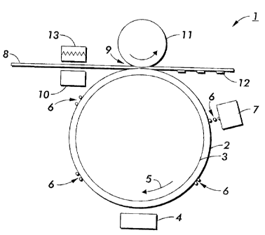
Referring to Figure 1, offset printing apparatus 1 is demonstrated to
show transfer of an ink image from the imaging member to a final printing
medium or receiving substrate. As the imaging member 3 turns in the
direction of arrow 5, a liquid surface 2 is deposited on imaging member 3.
The imaging member 3 is depicted in this embodiment as a drum
member. However, it should be understood that other embodiments can
be used, such as a belt member, film member, sheet member, or the like.
The liquid layer 2 is deposited by an applicator 4 that may be positioned at
any place, as long as the applicator 4 has the ability to make contact and
apply liquid surface 2 to imaging member 3.
The ink used in the printing process can be a phase change ink,
such as, for example, a solid ink. The term "phase change ink" means
that the ink can change phases, such as a solid ink becoming liquid ink or
changing from solid into a more malleable state. Specifically, in
embodiments, the ink can be in solid form initially, and then can be
changed to a molten state by the application of heat energy. The solid ink
may be solid at room temperature, or at about 25 C. The solid ink may
possess the ability to melt at relatively high temperatures above from
about 85 C to about 150 C. The ink is melted at a high temperature and
then the melted ink 6 is ejected from printhead 7 onto the liquid layer 2 of
imaging member 3. The ink is then cooled to an intermediate temperature
of from about 20 C to about 80 C, or about 72 C, and solidifies into a
-11-
CA 02451931 2008-02-15
malleable state in which it can then be transferred onto a final receiving
substrate 8 or print medium 8.
The ink has a viscosity of from about 5 to about 30 centipoise, or
from about 8 to about 20 centipoise, or from about 10 to about 15
centipoise at about 140 C. The surface tension of suitable inks is from
about 23 to about 50 dynes/cm. Examples of a suitable inks for use
herein include those described in U.S. Patent 4,889,560; 5,919,839;
6,174,937; and 6,309,453.
Some of the liquid layer 2 is transferred to the print medium 8 along
with the ink. A typical thickness of transferred liquid is about 100
angstroms to about 100 nanometer, or from about 0.1 to about 200
milligrams, or from about 0.5 to about 50 milligrams, or from about 1 to
about 10 milligrams per print medium.
Suitable liquids that may be used as the print liquid surface 2
include water, fluorinated oils, glycol, surfactants, mineral oil, silicone
oil,
functional oils, and the like, and mixtures thereof. Functional liquids
include silicone oils or polydimethylsiloxane oils having mercapto, fluoro,
hydride, hydroxy, and the like functionality.
Feed guide(s) 10 and 13 help to feed the print medium 8, such as
paper, transparency or the like, into the nip 9 formed between the
pressure member 11 (shown as a roller), and imaging member 3. It
should be understood that the pressure member can be in the form of a
belt, film, sheet, or other form. In embodiments, the print medium 8 is
heated prior to entering the nip 9 by heated feed guide 13. When the print
medium 8 is passed between the printing medium 3 and the pressure
member 11, the melted ink 6 now in a malleable state is transferred from
the imaging member 3 onto the print medium 8 in image configuration.
The final ink image 12 is spread, flattened, adhered, and fused or fixed to
the final print medium 8 as the print medium moves between nip 9.
Alternatively, there may be an additional or alternative heater or heaters
(not shown) positioned in association with offset printing apparatus 1. In
another embodiment, there may be a separate optional fusing station
-12-
CA 02451931 2008-02-15
located upstream or downstream of the feed guides.
The pressure exerted at the nip 9 is from about 10 to about 1,000
psi., or about 500 psi, or from about 200 to about 500 psi. This is
approximately twice the ink yield strength of about 250 psi at 50 C. In
embodiments, higher temperatures, such as from about 72 to about 75 C
can be used, and at the higher temperatures, the ink is softer. Once the
ink is transferred to the final print medium 8, it is cooled to an ambient
temperature of from about 20 C to about 25 C.
Stripper fingers (not shown) may be used to assist in removing the
print medium 8 having the ink image 12 formed thereon to a final receiving
tray (also not shown).
Figure 2 demonstrates an embodiment of the invention, wherein
imaging member 3 comprises substrate 15, having thereover outer coating
16 having nano-sized fillers 18 dispersed or contained therein.
Figure 3 depicts another embodiment of the invention. Figure 3
depicts a three-layer configuration comprising a substrate 15, intermediate
layer 17 positioned on the substrate 15, and outer layer 16 positioned on
the intermediate layer 17. Outer layer 16 comprises nano-size fillers 18
dispersed or contained therein. In embodiments, the substrate 15, and/or
intermediate layer 16 may comprise nano-size fillers. In embodiments, an
outer liquid layer 2 (as described above) may be present on the outer layer
16. In the Figures, the nano-size fillers are dramatically enlarged to show
them.
In embodiments, the outer layer comprises an elastomer, such as a
haloelastomer. Examples of elastomers comprising halogen monomers
include chloroelastomers, fluoroelastomers and the like. Examples of
fluoroelastomers include ethylenically unsaturated fluoroelastomers, and
fluoroelastomers comprising copolymers and terpolymers of
vinyl idenefluoride, hexafluoropropylene and tetrafluoroethylene, which are
known commercially under various designations as VITON A , VITON B ,
VITON E , VITON F , VITON E60C , VITON E45 , VITON E430 , VITON
B 910 , VITON GH , VITON B50 , VITON E45 , and VITON GF . The
-13-
CA 02451931 2008-02-15
VITON designation is a Trademark of E.I. DuPont de Nemours, Inc.
Three known fluoroelastomers are (1) a class of copolymers of
vinylidenefluoride, hexafluoropropylene and tetrafluoroethylene, known
commercially as VITON A , (2) a class of terpolymers of vinylidenefluoride,
hexafluoropropylene and tetrafluoroethylene known commercially as
VITON B , and (3) a class of tetrapolymers of vinylidenefluoride,
hexafluoropropylene, tetrafluoroethylene and a cure site monomer, for
example, VITON GF.
In another embodiment, the fluoroelastomer is a tetrapolymer
having a relatively low quantity of vinylidenefluoride. An example is VITON
GF , available from E.I. DuPont de Nemours, Inc. The VITON GF has 35
weight percent of vinylidenefluoride, 34 weight percent of
hexafluoropropylene and 29 weight percent of tetrafluoroethylene with 2
weight percent cure site monomer. The cure site monomer can be those
available from DuPont such as 4-bromoperfluorobutene-1, 1,1-dihydro-4-
bromoperfluorobutene-1, 3-bromoperfluoropropene-1, 1,1-dihydro-3-
bromoperfluoropropene-1, or any other suitable, known, commercially
available cure site monomer.
Other fluoroelastomers that may be used include AFLAS ,
FLUOREL I, FLUOREL II, TECHNOFLON and the like commercially
available elastomers.
In embodiments, the outer layer may comprise a hybrid elastomer, a
blend, a thermoplastic material, thermosetting material, a haloelastomer
having pendant chains, a fluorosilicone material, a latex fluoroelastomer, a
mica-type silicate material, a Q-resin, or other like material as described in
the applications cited in the "Cross Reference to Related Applications."
The hardness of the outer layer is typically from about 10 to about
95 Shore A, or from about 60 to about 95 Shore A.
In embodiments, the thickness of the outer layer is from about 5 to
about 250 microns, or from about 15 to about 150 microns, or from about
20 to about 25 microns.
In embodiments, the outer layer comprises a nano-size filler
-14-
CA 02451931 2008-02-15
dispersed or contained therein. The substrate, optional intermediate layer,
and/or outer layer, in embodiments, can comprise nano-size fillers
dispersed therein. These fillers can have the ability to increase the
material hardness or modulus into the desired range.
Examples of nano-size fillers include fillers having an average
particle size of from about 1 to about 250 nanometers, or from about 5 to
about 150 nanometers, or from about 10 to about 100 nanometers, or
from about 20 to about 50 nanometers. Suitable nano-size fillers include
fillers such as metals, metal oxides, carbon blacks, polymers, and sol-gel
particles, and mixtures thereof, as long as they are nano-size. Examples
of suitable nano-size metal oxide fillers include nano-size silicon oxide,
aluminum oxide, chromium oxide, zirconium oxide, zinc oxide, tin oxide,
iron oxide, magnesium oxide, manganese oxide, nickel oxide, copper
oxide, conductive antimony pentoxide and indium tin oxide, and the like,
and mixtures thereof. Other examples of nano-size fillers include high
(HAF) or super (SAF) abrasion carbon black particles such as carbon
black N110, N220, N330, N550 and N660, Regal 999, and conductive XC-
72; thermally conducting carbon fillers; oxidized and reduced C 975U
carbon black from Columbian and fluorinated carbon black such as
ACCUFLUOR or CARBOFLUOR , and the like, and mixtures thereof.
Examples of nano-size silica include silica from Degussa AerosilTM 90,
AerosilTM 130, AerosilTM 150, OX50, and PDMS coated L90 from Cabot,
and the like and mixtures thereof. Examples of nano-sized polymer fillers
include polytetrafluoroethylene, nano-size Q-resin and T-resin, polyimide,
polyphenylene sulfide, poly(ether ether ketone), and the like, and mixtures
thereof. Suitable metal oxides include those made by the sol-gel process.
Examples of sol-gel nano-size particles include hydrolyzed metal
alkoxides or aryloxides such as tetraalkoxy orthosilicates, titanium
isbutoxide, and the like, and mixtures thereof.
The sol-gel particles may be grown inside the outer layer elastomer,
in embodiments. The chemistry of the sol-gel process is shown below:
-15-
CA 02451931 2008-02-15
CF3
Si(OR)4 + -CF2CH2CFCF2CF2-
(Viton )
Hydrolysis Hp
Condensation
O R
O-Si-O
I Si_O__
O R n
In the above scheme, n is a number of from about 1 to about 200,
or from about 1 to about 50, or from about 1 to about 25.
In embodiments, the nano-size particles may be prepared in the
elastomer matrix, by dissolving an effective amount of the elastomer, for
example, from about 1 to about 35 percent by weight, or from about 5 to
about 15 percent by weight of total solids, in an effective amount of a
suitable solvent, such as an aliphatic hydrocarbon including for example
methyl ethyl ketone, methyl isobutyl ketone, and the like, at any effective
temperature, such as 25 C. Acetic acid catalyst is added in an effective
amount, for example, from about 1 to about 15 percent by weight, or from
about 3 to about 10 percent by weight relative to the weight of the
elastomer, followed by stirring of the solution for about 15 to about 60
minutes at a temperature of about 45 C to about 100 C. An effective
amount of a silane compound such as tetraethoxyorthosilicate, for
example, from about 1 to about 75 percent by weight, or from about 5 to
about 50 percent by weight relative to the weight of elastomer, is then
added and heating is continued at a temperature of about 4 C to about
100 C. for an additional 20 minutes to about 10 hours. Any effective
sequence of addition of the various components may be used to prepare
this composition. For example, in embodiments, the elastomer may be
-16-
CA 02451931 2008-02-15
added to a solvent already containing the acetic acid and/or the silane
compound. The time of reaction is about 4 hours at about 65 C.
In embodiments, the process to prepare the nano-size silica
particles in a elastomer matrix may also include other components to
facilitate the preparation thereof. For example, a nucleophilic curing agent
for the elastomer such as VITON Curative No. 50 and diamines such as
Diac available from E.I. Dupont deNemours, Inc. may be employed at an
effective concentration, such as from about 1 to about 15 percent by
weight, or from about 2 to about 10 percent by weight, relative to the
weight of the elastomer. VITON Curative No. 50, which incorporates an
accelerator (a quaternary phosphonium salt or salts) and a crosslinking
agent, such as bisphenol AF in a single curative system, may be added in
a 3 to 7 percent solution predissolved to the elastomer compound. Also,
the basic oxides such as MgO and/or Ca(OH)2 in effective amounts, such
as from about 0.5 to about 10 percent by weight, or from about 1 to about
3 percent by weight, relative to the weight of the elastomer, may be added
in particulate form to the solution mixture.
The above mixture including the curative and the oxides, is then
ball milled for about 2 to about 24 hours or from about 5 to about 15 hours
to obtain a fine dispersion of the oxides. The curative component can also
be added after ball milling in a solution form. The solution of the curative
is
generally prepared by dissolving VITON Curative No. 50 in methyl ethyl
ketone ("MEK") or methyl isobutyl ketone ("MIBK"). The concentration of
the solids, can vary from about 5 percent to about 25 percent by weight or
from about 10 to about 15 percent by weight.
Providing an effective layer of the polymer composite with nano-
size silica particles on the substrate may be accomplished by any suitable
known method such as by spraying, dipping, flow, web or the like to a level
of film of from about 10 to about 150 microns in thickness or from about
50 to about 100 microns in thickness. The thickness of the overcoating is
selected to provide a layer thick enough to allow a reasonable wear life.
While molding, extruding and wrapping techniques are alternative means
-17-
CA 02451931 2008-02-15
that may be used, in embodiments, flow coating of successive
applications of the dispersion can be used. When the desired thickness of
coating is obtained, the coating is cured, by any suitable known method,
and thereby bonded to the surface. A typical step curing process is
heating for about 2 hours at about 93 C, followed by about 2 hours at
about 149 C, followed by about 2 hours at about 177 C, followed by about
16 hours at about 208 C.
The nano-size filler may be present in the substrate, optional
intermediate layer, and/or outer layer in an amount of from about 1 to
about 50 percent, or from about 1 to about 30 percent by weight of total
solids in the layer. Total solids by weight, as used herein, refers to the
total amount by weight of outer layer elastomer, fillers, additives, and any
other solids.
The nano-size fillers provide antistatic properties to the outer layer
in a highly conductive range of from about 104 to about 1012 ohm-cm or
from about 108 to about 1010 ohm-cm.
The imaging substrate can comprise any material having suitable
strength for use as an imaging member substrate. Examples of suitable
materials for the substrate include metals, fiberglass composites, rubbers,
and fabrics. Examples of metals include steel, aluminum, nickel, and their
alloys, and like metals, and alloys of like metals. The thickness of the
substrate can be set appropriate to the type of imaging member
employed. In embodiments wherein the substrate is a belt, film, sheet or
the like, the thickness can be from about .5 to about 500 mils, or from
about 1 to about 250 mils. In embodiments wherein the substrate is in the
form of a drum, the thickness can be from about 1/32 to about 1 inch, or
from about 1/16 to about 5/8 inch.
Examples of suitable imaging substrates include a sheet, a film, a
web, a foil, a strip, a coil, a cylinder, a drum, an endless strip, a circular
disc, a belt including an endless belt, an endless seamed flexible belt, an
endless seamless flexible belt, an endless belt having a puzzle cut seam,
a weldable seam, and the like.
-18-
CA 02451931 2008-02-15
In an optional embodiment, an intermediate layer may be
positioned between the imaging substrate and the outer layer. Materials
suitable for use in the intermediate layer include silicone materials,
elastomers such as fluoroelastomers, fluorosilicones, ethylene propylene
diene rubbers, and the like, and mixtures thereof. In embodiments, the
intermediate layer is conformable and is of a thickness of from about 2 to
about 60 mils, or from about 4 to about 25 mils.
The nano-size filled coating has the superior qualities of the
elastomeric coatings, and also increased wear and life. The nano-size filled
coating also provides improved surface wear resistance and improved
gloss maintenance life against paper abrasion.
Specific embodiments of the invention will now be described in
detail. These examples are intended to be illustrative, and the invention is
not limited to the materials, conditions, or process parameters set forth in
these embodiments. All parts are percentages by weight of total solids as
defined above unless otherwise indicated.
EXAMPLES
Example I
Preparation of Nano-sized Filled Fluoroelastomer Imaging Member Outer
Layer
An aluminum substrate imaging member having the dimensions of
about 10 inches long, about 4 inches in diameter, and about 0.25 inches
thick, was first sanded with 400 grit sand paper, and cleaned with methyl
ethyl ketone. The cleaned drum was then air dried, followed by
compressed air treatment to remove residual dust particles. The cleaned
drum was then coated uniformly with about 3 grams of a primer solution of
ChemlokT"" 5150 primer (an amino silane as identified by the
manufacturer) solution (9:1 dilution with methanol), and allowed for
hydrolysis. The primed aluminum base drum was then air dried and
allowed for further primer hydrolysis for at least 30 minutes. The primed
drum was usually coated within 48 hours of primer application.
-19-
CA 02451931 2008-02-15
A fluoroelastomer outer coating solution was prepared by mixing a
fluoroelastomer (such as VITON GF, VITON B50, TECHNOFLON
P959, or the like), comprising a curative (VC-50, Diak III, or A0700),
curative base metal oxides (magnesium oxide and/or calcium hydroxide)
and nano-size fillers.
In an embodiment, VITON B50 from DuPont Dow Elastomers was
added at 100 pph, along with 17.5 pph of nano-size silica AerosilTM 130
from Degussa, Akron, Ohio (having a 20 nanometer filler particle size), 1.5
pph additive (N-330 carbon black colorant from R.T. Vanderbilt Company,
Inc. Norwalk, Connecticut), 5 pph VC-50 curative, 2 pph MgO, and 1 pph
Ca(OH)2. The mixture was then mixed with a paint-shaker until a uniform
solution was obtained. The coating with the above fluoroelastomer
solution having the nano-size filler was flow coated onto an imaging drum
as described above, to a weight based thickness of from about 15 to about
100 microns. The percent extractables were less than about 5 percent, and
the surface roughness was less than about 0.2 microns.
After the coating was air dried overnight, the coated imaging
member was oven dried at 120 F for about 4 hours, followed by step heat
curing at 200 F for 2 hours, 300 F for 2 hours, 350 F for 2 hours, 400 F for
2 hours, and 450 F for 6 hours. The final elastomer thickness was from
about 15 to about 150 microns. The cured imaging member was then
cooled to room temperature and ready for print testing.
The following Table 1 shows the materials and amounts used.
Table 1
. .. ... .
Base elastomer Viton TM B50 100 pph
Base filler Nano-sized A130 17.5 pph
Filler particle size -20 nm
Additive N-330 CB colorant 1.5 pph
Curative & catalyst VC-50 5.0 pph
Base metal oxide 1 M O 2.0 pph
Base metal oxide 2 Ca OH Z 1.0 pph
Weight Based Thickness 20-25 Demonstrated
% Extractables <5% 160K prints average
-20-
CA 02451931 2008-02-15
= == =.= =
Surface roughness, R. <0.2 life of machine
Comparative Example 2
Preparation of Imaging Member Fluoroelastomer Outer Coating with Sub-
micron-sized Filler
The process for making a fluoroelastomer filled outer layer as in
Example 1 was repeated, except that the following materials and amounts
shown in Table 2, were substituted for the above ingredients shown in
Table 1. The base filler was changed from a nano-size filler to a
submicron-size filler, and the amount was increased for the submicron-size
filler to 75 pph from 17.5 pph. Also, the additive was changed from a
carbon black colorant at 1.5 pph, to a VITON Graft additive at 55 pph. In
addition, the base elastomer was changed from VITON B50 to VITON
GF.
Table 2
Components Materials Loading
Base elastomer VitonTM GF 100 pph
Base filler N-990 Carbon Blank 75 pph
Filler particle size -0.5 p
Additive Viton Graft 55 pph
Curative & catalyst VC-50 5.0 pph
Base metal oxide 1 M O 2.0 pph
Base metal oxide 2 Ca OH 2 1.0 pph
Weight based thickness (p) 40 Gloss life
% Extractables <10% (-50K prints)
Surface roughness, Ra (p) -0.2 shortfall
Example 3
Testing of the Fluoroelastomer Imaging Drum Coatings
The coated drums prepared in accordance with Examples 1 and 2
were tested in modified Phaser 860 lab solid ink printers.
The results are shown in Table 3 below.
-21-
CA 02451931 2008-02-15
Table 3
Imaging Member Number of prints with acceptable
image gloss level
Example 1 (nano-sized filler) 160,000 prints
Comparative Example 2 (submicron 50,000 prints
filler)
The above results from Table 3 demonstrate that by use of the
nano-size fillers, the imaging drum printed acceptable image gloss prints
for the life of the machine, or 160,000 prints. Conversely, the imaging
drum with the coating having submicron-size particles provided unfavorable
results, and only printed 50,000 acceptable image gloss level prints.
The coating having the nano-size filler provides, in embodiments,
control of surface roughness, lower coefficient of friction, less surface
damage, durability against paper handling, and improved gloss life.
Example 4
Preparation of Sol-gel Nano-size Silica Particles in VITON GF Laver
An aluminum substrate imaging member having the dimensions of
about 10 inches long, about 4 inches in diameter, and about 0.25 inches
thick, was first sanded with 400 grit sand paper, and cleaned with methyl
ethyl ketone. The cleaned drum was then air dried, followed by treatment
with compressed air to remove residual dust particles. The cleaned drum
was then coated uniformly with about 3 grams of a primer solution of
ChemlokT"" 5150 primer (an amino silane as identified by the
manufacturer) solution (9:1 dilution with methanol), and allowed for
hydrolysis. The primed aluminum base drum was then air dried and
allowed for further primer hydrolysis for at least 30 minutes. The primed
drum was usually coated within 48 hours of primer application.
The polymer nanocomposite composition containing nano-size silica
particles was prepared as follows. A stock solution of VITON GF was
prepared by dissolving 250 g of VITON GF in 2.5 liters of methylethyl
-22-
CA 02451931 2008-02-15
ketone (MEK) with stirring at room temperature. A four liter plastic bottle
and a moving base shaker were used to prepare the stock solution.
Approximately one hour to two hours was used to accomplish the
dissolution. The above solution was then transferred to a four-liter
Erlenmeyer flask and 25 ml of glacial acetic acid, which can be obtained
from VWR Scientific Products of Cincinnati, Ohio. The contents of the flask
were then stirred using a mechanical stirrer while maintaining the
temperature between 55 C and 60 C. After stirring for 30 minutes, 12.5
grams of tetraethoxyorthosilicate (TEOS), available from Huls America Inc.,
was added and stirring continued for another five minutes. To this mixture,
another aliquot of 12.5 grams of tetraethoxyorthosilicate (TEOS) was
added followed by 25 mils of acetic acid. The stirring was continued while
heating the contents of the flask at around 65 C for another 4 hours. The
contents of the flask were then cooled to room temperature.
Subsequently, 5 grams of magnesium oxide, 2.5 grams of calcium
hydroxide and 12.5 grams of curative VC-50 available from Dow Chemical
Co. were added. The above contents were then ball jarred with ceramic
balls as media for 17 hours. This dispersion was then flow coated onto an
imaging drum substrate. The dry film was then cured by the following
heating procedure: 2 hours at 93 C, 2 hours at 149 C, 2 hours at 177 C,
and thereafter heating for 16 hours at 208 C. The thickness of the cured
film as determined by permoscope was found to be about 4 mils.
Example 5
Preparation of Sol-gel Nano-size Titania Particles in VITON GF Layer
For precipitating nano size titania particles in the VITON GF matrix,
the procedure of Example 4 was repeated with the exception that instead
of tetraethoxyorthosilicate, 12.5 grams of titanium isobutoxide was used.
The final thinkness of the coating was determined to be about 3 mils.
Example 6
Preparation of Sol-gel Nano-size Silica Particles in VITON GF Layer
-23-
CA 02451931 2008-02-15
The procedure of Example 4 was repeated with the exception that
the amount of tetraethoxyorthosilicate was 37.5 grams. A dry cured film of
about 5 mils thickness was obtained.
Example 7
Preparation of Sol-gel Nano-size Titania Particles in VITON GF Layer
The procedure of Example 5 was repeated with the exception that
the amount of titanium isobutoxide was 50 grams. A dry cured film of about
6 mils thickness was obtained.
While the invention has been described in detail with reference to
specific and preferred embodiments, it will be appreciated that various
modifications and variations will be apparent to the artisan. All such
modifications and embodiments as may readily occur to one skilled in the
art are intended to be within the scope of the appended claims.
-24-