Note: Descriptions are shown in the official language in which they were submitted.
CA 02452519 2003-12-04
1 CA,CN,EP,KR,TW,US-X0626
PACKAGE FOR HOUSING SEMICONDUCTOR CHIP, FABRICATION METHOD
THEREOF AND SEMICONDUCTOR DEVICE
BACKGROUND OF THE INVENTION
1. Field of the Invention
[0001 The present invention relates to a package for
housing semiconductor integrated circuit chips such as ICs and
LSIs, as well as field effect transistors (FET: Field Effect
Transistor) or a variety of other semiconductor chips, and more
particularly to a package for housing a semiconductor chip used
in high power, high frequency transistors and power amplifiers
for electrical/electronic components in telecommunication
base station, as well as to a semiconductor device employing
this package for housing semiconductor chip.
2. Description of the Related Art
[0002] A wireless semiconductor package, which is one
type of conventional package for housing semiconductor chip
(referred to as semiconductor package hereinbelow), is formed
such that a thermal diffusion substrate is mounted on a
rectangular parallelepiped-shaped metal substrate and a
semiconductor chip is mounted atop the thermal diffusion
substrate.
[0003] According to the enhanced autput of semiconductor
chips in recent years, the applied power has increased, and the
amount of heat generated has also steadily increased.
Accordingly, measures have been taken to improve the
performance about cooling chips by adopting a high thermal
conductive material such as a Cu or Cu-W composite material for
the metal substrate and heat-spreasing substrate. More
particularly, where the most recent forms of package are
CA 02452519 2003-12-04
2 CA,CN,EP,KR,TW,US-10626
concerned, a package produced by forming a ceramic wall on a
Cu-W composite alloy substrate so that this ceramic wall
encloses the semiconductor chip, and then mounting an
input/output terminal on this ceramic wall has become
mainstream.
[0004] This type of package is introduced in Japanese
Patent Publication No. H4-65544B. According to the description
in this publication, in a thermal conductive substrate
consisting of a copper-tungsten and/or copper-molybdenum
composite material, by using a composite material whose copper
content is equal to or less than 30~ mass as the thermal
conductive substrate, the ceramic, which constitutes a package
circumferential member, is not damaged. And, by using a
composite material whose copper content is equal to or less than
25 o mass, practical use is unproblematic even when the thermal
conductive substrate and circumferential member that consists
of ceramic are directly connected by brazing material.
[0005] In addition, Japanese Patent Publication No.
2002-121639A reports on a procedure for optimizing Young's
modulus while retaining the thermal conductivity by adjusting
the amount of ferrous metal contained in addition to
controlling the amount of copper in the material. Because, in
a thermal conductive substrate consisting of a copper-tungsten
and/or copper-molybdenum composite material, when the copper
content is less than 25o mass, the rigidity of the substrate
itself increases. Consequently, in the case of a package with
a large heat-generating chip in particular, when a considerably
thick brazing material layer or stress alleviation layer is not
interposed between the connecting sections of the package, this
layer sometimes does not withstand the heat-cycles during
application.
[0006] Japanese Patent Publication No. 2001-244357A
introduces a semiconductor housing package where the stress is
laid on economic efficiency while at the same time ensuring high
CA 02452519 2003-12-04
3 CA,CN,EP,KR,TW,US-10626
thermal conductivity by applying a diamond and/or diamond-
coated substrate only directly below the semiconductor chip
mounting space.
[0007] However, the amount of heat that is generated
during operation, in depending on the further enhancements of
the output of semiconductor chips in recent years is gradually
increasing, and this heat builds up rather than being diffused.
As a result, the operability of the semiconductor chip is
compromised, and there is the problem of thermal degradation.
As means for resolving this problem, although consideration may
also be paid to adding cooling equipment to the outside and
increasing the size to raise the thermal conduction efficiency,
in this case, the electrical power consumption of the enclosure
for housing the semiconductor package increases or the
enclosure is enlarged, which represents a deviation from the
recent trend toward miniaturization, a lighter weight and
reduced electrical power consumption.
[0008] Further, a package employing a diamond and/or
diamond thin film substrate is highly effective in spreading
heat generated locally by the semiconductor chip.
However, the possibility exists that the performance of cooling
chips will be inferior to the increased amount of heat
generation in the future, particularly in a system in which heat
is diffused (conducted) to the outside of the package, because
this package has a constitution in which a substrate whose
thermal conductivity is inferior to that of diamond and a
diamond thin film substrate is disposed. In addition, with
regard to a monocrystalline diamond that is larger than the
semiconductor chip or a monocrystalline/polycrystalline
diamond formed by chemical vapor deposition (CVD), and a
diamond thin film substrate formed by chemical vapor deposition,
the synthesis costs and the costs involved in machining the
shape of the substrate surface to a level permitting the
semiconductor chip to be mounted thereon cannot be adequately
CA 02452519 2003-12-04
c~
4 CA,CN,EP,KR,TW,US-10626
cut, and hence, from an economical perspective, usage is
restricted to special applications.
[0009] These problems are not limited to the above
semiconductor package, being equally related to semiconductor
packages that allow the substrate to function as a heat
spreading plate and that house semiconductor integrated
circuit chips such as ICs and LSIs ~ as well as FETs or a variety
of other semiconductor chips.
SUN~tARY OF THE INVENTION
(0010] Accordingly, the present invention was completed
in view of the foregoing problems, an object thereof being to
provide an economical package for housing semiconductor chip
that allows a semiconductor chip to operate normally and stably
over long periods by efficiently transferring heat generated
during the operation of semiconductor integrated circuit chips
such as ICs and LSIs, as well as a variety of semiconductor chips
such as FETs, LDs, LEDs and PDs, and particularly high-power,
high frequency transistors, to the package mount substrate.
(0011] The present invention was completed when, as a
result of the present inventors carrying out a thorough
investigation, they discovered that the above problems can be
resolved by enhancing the substrate, the constitution of this
invention being as follows:
[0012] (1) A package for housing semiconductor chip
comprising:
a substrate, whose upper face is provided with a mounting
space whereon a semiconductor chip is mounted, and whose
opposite sides are provided with a screw mounting part that is
a through-hole or notch, and at least a portion of the substrate
below the mounting space comprising
a metal-diamond composite comprising diamond
grains,
CA 02452519 2003-12-04
CA,CN,EP,KR,TW,US-10626
a metal carbide covering a surface of the diamond
grains, and
a metal containing silver and/or copper as a main
component and laying between the diamond grains by
infiltrating therebetween, and
wherein, a remaining part that includes the screw
mounting part consists of a metal~
a frame on the upper face of the substrate so as to
surround the mounting space, the frame having a joint for an
input/output terminal at a side or top thereof; and
an input/output terminal being connected to the joint.
[0013] (2) A package for housing semiconductor chip
according to ( 1 ) above, wherein at least a portion of a surface
of said substrate comprising the metal and the metal-diamond
composite, and/or a portion of a surface of said frame, and/or
a portion of a surface of said input/output terminal is plated
with gold.
[0014] (3) A package for housing semiconductor chip
according to (1) or {2) above, wherein the metal of the
substrate, which comprises the metal and the metal-diamond
composite, is a metal or a metal alloy containing at least one
element selected from Cu, Fe, Mo, W, Ni, Co and Cr.
[0015] (4) A package for housing semiconductor chip
according to any of {1) to (3) above, wherein a thermal
expansion coefficient of the metal of said substrate, which
comprises the metal and the metal-diamond composite, is the
same as or greater than a thermal expansion coefficient of the
metal-diamond composite.
[0016] (5) A package for housing semiconductor chip
according to any of {1) to (4) above, wherein a method for
joining said metal and said metal-diamond composite is brazing.
[0017] (6) A package for housing semiconductor chip
according to any of (1) to (4) above, wherein a method for
joining said metal and said metal-diamond composite is a method
CA 02452519 2003-12-04
6 CA,CN,EP,KR,TW,US-10626
involving diffusion of the metals.
[0018] (7) A package for housing semiconductor chip
according to any of (1) to (4) above, wherein a method for
joining said metal and said metal-diamond composite is
tight-fit bonding.
[0019] (8) A package for housing semiconductor chip
according to any of ( 1 ) to ( 7 ) above, wherein an average grain
diameter of the diamond grains is 10 to 700 Vim.
[0020] (9) A package for housing semiconductor chip
according to any of ( 1 ) to ( 8 ) above, wherein an average grain
diameter of the diamond grains is 50 to 700 pm at the center
of the metal-diamond composite and 10 to 60 um at the
circumference thereof.
[0021] (10) A semiconductor device comprising:
the package for housing semiconductor chip according to
any of (1) to (9) above;
a semiconductor chip being mounted on and fixed to the
mounting space; and
a lid being joined to an upper face of the frame.
[0022] (11) A method for fabricating a package for
housing semiconductor chip comprising:
inserting a metal-diamond composite into part of a hole
in a metal substrate provided with a hole, the metal-diamond
composite comprising diamond grains whose surface is covered
with a metal carbide and a metal containing silver and/or copper
as a main component and the metal laying between the diamond
grains by infiltrating therebetween; and
joining the metal substrate and the metal-diamond
composite together to form a substrate;
providing a mounting space to mount a semiconductor chip
on an upper face of the substrate;
providing a screw mounting part that is a through-hole
or notch at opposite sides of the substrate; and
assembling the substrate, a frame to be on the upper face
CA 02452519 2003-12-04
7 CA,CN,EP,KR,TW,~15-10626
of the substrate so as to surround the mounting space and having
a joint for an input/output terminal at a side or top thereof,
and an input/output terminal to be connected to the joint.
[0023] (12) A method for fabricating a package for
housing semiconductor chip comprising:
filling diamond grains, a powder of a metal containing
copper and/or silver as a main component and a powder of a metal
used to form a carbide, into a hole in a metal substrate provided
with a hole;
packing a mixture of the diamond grains and the metal
powders so that the diamond grains and the metal powders are
distributed at a uniform density;
heating the packed mixture so as to form a metal-
composite in which a carbide covers a surface of the diamond
grains, and to join the metal-diamond composite and the metal
substrate together to form a substrate, by allowing the metal
containing copper and/or silver as a main component to
infiltrate a gap in the powders;
providing a mounting space to mount a semiconductor chip
on an upper face of the substrate;
providing a screw mounting part that is a through-hole
or notch at opposite sides of the substrate; and
assembling the substrate, a frame to be on the upper face
of the substrate so as to surround the mounting space and having
a joint for an input/output terminal at a side or top thereof,
and an input/output terminal to be connected to the joint;
[0024] (13) A method for fabricating a package for
housing semiconductor chip comprising:
press-molding a diamond grains, a powder of a metal
containing copper and/or silver as a main component and a powder
of a metal used to form a carbide, so as to form a temporary
molded body in which the diamond grains and the metal powders
are distributed at a uniform density;
filling the temporary molded body into a hole in a metal
CA 02452519 2003-12-04
8 CA,CN,EP,KR,TW;US-10626
substrate provided with a hole;
allowing the powder of a metal containing copper and/or
silver as a main component to infiltrate the temporary molded
body so as to form a metal-diamond composite in which a carbide
covers a surface of the diamond grains, and to join the
metal-diamond composite and the metal substrate together, for
obtaining a substrate;
providing a mounting space to mount a semiconductor chip
on an upper face of the substrate;
providing a screw mounting part that is a through-hole
or notch at opposite sides of the substrate; and
assembling the substrate, a frame to be on the upper face
of the substrate so as to surround the mounting space and having
a joint for an input/output terminal at a side or top thereof,
and an input/output terminal to be connected to the joint.
[0025] (14) A method for fabricating a package for
housing semiconductor chip according to ( 13 ) above, wherein the
temporary molded body is sandwiched between a molded bodies of
the powder of a metal containing copper and/or silver as a main
component, and then the metal containing copper and/or silver
as a main component is allowed to infiltrate the temporary
molded body by heating.
[0026] According to the constitution in ( 1 ) and ( 2 ) above,
the semiconductor package can be rigidly bonded to an external
electrical circuit, and, even when the amount of heat generated
during operation of the semiconductor chip is extremely large,
this heat can be efficiently transferred to a heat sink, and,
by forming a gold plated layer, which is a stable material,
degradation with respect to humidity and so forth can also be
suppressed, and the semiconductor chip housed within the
semiconductor package can be allowed to operate normally and
stably over long periods.
[ 0027 ] As for the substrate that comprises a metal and a
metal-diamond composite, because a metal or metal alloy
CA 02452519 2003-12-04
9 C~-1,CN,EP,KR,TW,US-10626
including at least one element of Cu, Fe, Mo, W, Ni, Co and Cr
is used as the metal, a raw material cost reduction greater than
when the whole body is the metal-diamond composite can be
achieved. Furthermore, metal machining in which the
workability of the external form that is also generally used
can be applied. A reduction in the machining costs as well as
a shortage of the machining time can be achieved by omitting
the special machining steps arising from the inclusion of
diamond, then a package cost reduction is possible.
[0028] In the package of the present invention, because
the thermal expansion coefficient of the metal of the substrate
comprising a metal and a metal-diamond composite is the same
as or larger than the thermal expansion coefficient of the
metal-diamond composite, cracks do not occur at the interface
between the metal of the substrate and the metal-diamond
composite, even though a temperature rises when joining the
semiconductor chip to the mounting space of the substrate by
using a gold solder and the temperature drops after mounting.
[0029] Moreover, according to the package of the present
invention, because brazing is employed as the method for
joining the metal portion of the substrate comprising a metal
and a metal-diamond composite, with the metal-diamond
composite, a rigid join can be achieved.
(0030] In the package of the present invention, because
the method for joining the metal-diamond composite to the metal
portion of the substrate which comprises a metal and a
metal-diamond composite is implemented via the diffusion of the
metals, a rigid join can be achieved. And, the characteristics
such as the thermal expansion coefficient close to the end of
the interface, the thermal conductivity, and so forth, are the
intermediate characteristics of the metal and the metal-
diamond composite. A concentration of thermal stress can also
be alleviated with respect to temperature variations due to the
rise and fall in temperature during mounting of the
CA 02452519 2003-12-04
CA,CN,EP,KR,TW,US-10626
semiconductor chip, thermal shock, temperature cycle tests and
so forth.
[0031] About the package of the present invention, the
method for joining the metal-diamond composite to the metal
section of the substrate which comprises a metal and a
metal-diamond composite permits a rigid join by means of
tight-fit bonding.
[0032] In the package of the present invention, because
the average grain diameter of a diamond grain is 10 to 700 ,um,
the metal-diamond composite can be afforded a moderate thermal
expansion coefficient. When this diameter is less than 10 Vim,
a sufficient thermal conductivity is not obtained because a
multiplicity of diamond grains lining up in the thermal
conduction path from the upper face of the substrate to the
bottom face thereof and an increase in the metal layer lying
between the grains is caused. Meanwhile, when the average grain
diameter is larger than 700 Vim, only one or two diamond grains
can be included when the thickness of the substrate is about
1.4 mm, and the thermal expansion coefficient of the metal-
diamond composite is close to the thermal expansion coefficient
of diamond, meaning that the difference from the thermal
expansion coefficient of the semiconductor chip being mounted
is large.
[0033] Furthermore, in the package of the present
invention, by making the average grain diameter of the diamond
grains 50 to 700 pm at the center of the metal-diamond composite
and 10 to 60 um at the circumference, the thermal conductivity
can be raised and damage to the metallic mold can be reduced.
That is, by arranging diamond grains of a relatively large
diameter at the center, the thermal conductivity can be raised.
Also, by arranging diamond grains of a relatively small
diameter at the circumference, damage to the metallic mold in
the process of manufacturing the metal-diamond composite can
be reduced and surface roughness in the vicinity of the upper
CA 02452519 2003-12-04
11 CA,CN,EP,KR,TW,US-10626
and lower faces of the substrate can be diminished.
[0034] Moreover, a semiconductor device of the present
invention is equipped with the above-described package for
housing semiconductor chip of the present invention; a
semiconductor chip, which is mounted on and fixed to the
mounting space and electrically connected to the input/output
terminal; and a lid that is joined to the upper surface of a
frame, whereby a highly reliable semiconductor device
employing the semiconductor package can be provided.
BRIEF DESCRIPTION OF THE DRAWINGS
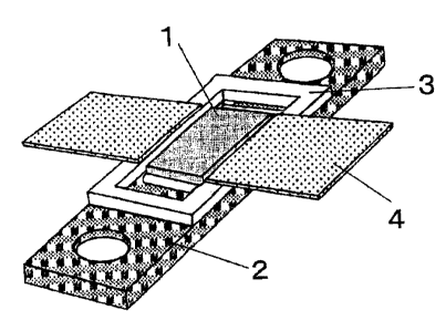
[0035] Fig. 1 is a perspective view of an example of the
package for housing semiconductor chip of the present
invention.
[0036] Fig. 2 provides a top view and cross-sectional view
of the package for housing semiconductor chip in Fig. 1.
[0037) Fig. 3 is an upper view of the parts of the package
for housing semiconductor chip in Fig. 1.
[0038] Fig. 4 is an enlarged cross-sectional view of the
metal-diamond composite.
[0039] Fig. 5 shows an example of the fabrication method
for the metal-diamond composite in the present invention.
[0040) Fig. 6 shows an example of the fabrication method
for the metal-diamond composite according to the present
invention;
[0041] Fig. 7 shows the state of the join between the
substrate and metal-diamond composite when a tapered hole is
provided in the substrate.
[0042] Fig. 8 shows the state of the join between the metal
and the metal-diamond composite.
DETAILED DESCRIPTION OF THE PREFERRED EMBODIMENTS
CA 02452519 2003-12-04
12 CA,CN,EP,KR,TW,US-10626
[0043] The package for housing semiconductor chip
according to the present invention will be described in detail
below. Figs. 1 to 3 show an example of the embodiment of the
semiconductor package of the present invention. Fig. 1 is a
perspective view of the semiconductor package, Fig. 2 provides
a top view and cross-sectional view of the substrate of the
semiconductor package, and Fig. 3 is an upper view of the parts
of the semiconductor package.
[0044] In Figs. 1 to 3, 1 is a semiconductor chip that is
mounted on and fixed onto a section 2d that is formed from the
metal-diamond composite of a substrate 2. 2 is the substrate,
3 is a frame, and 4 is an input/output terminal that is connected
to a joint 3a of the frame 3, the container for housing the
semiconductor chip being mainly constituted by the substrate
2, the frame 3, and the input/output terminal 4. In the
substrate 2, 2a denotes the metal portion, 2b denotes the screw
mounting part, 2c denotes the semiconductor chip mounting space,
and 2d denotes the metal-diamond composite.
[0045] Moreover, Fig. 4 is an enlarged cross-sectional
view of the metal-diamond composite, the metal-diamond
composite comprises diamond grains d, metal carbide m, and a
metal n that contains copper and/or silver as a main component.
The surface of the metal-diamond composite preferably has a
gold plated layer (n layer) deposited thereon.
[0046] The thermal expansion coefficient of the metal-
diamond composite employed by the present invention is 5 to
10x10-6/°C as a result of the metal-diamond composite being
infiltrated with a metal whose principal constituents)
is(are) copper and/or silver. Copper and/or silver is used as
the metal with which the metal-diamond composite is infiltrated
because of virtue of the characteristics of copper and/or
silver, the thermal expansion coefficient being 17 to
20x10-6/°C, the thermal conductivity being not less than 390
W/m~K, the modulus of elasticity being not less than 80 GPa,
CA 02452519 2003-12-04
13 CA,CN,EP,KR,TW,US-10626
and the melting point being not less than 900 °C. These
characteristics are preferable from the perspective of the
fabrication and characteristics of the semiconductor package.
[0047] Describing this specifically, where the thermal
expansion coefficient is concerned, if the base matrix in which
diamond grains are joined via a metal carbide is infiltrated
at an appropriate volume with a metal containing copper and/or
silver as the main component, the thermal expansion coefficient
of the metal-diamond composite does not rise to an extent where
same differs greatly from that of the semiconductor chip.
Moreover, there is the advantage that the heat generated during
operation of the semiconductor chip is transmitted because the
thermal conductivity of copper and silver is extremely high.
[0048] In addition, because the melting point of the metal
whose principal component is copper and/or silver is extremely
high, no melting of the semiconductor package occurs even when
same is assembled by means of silver brazing material or another
brazing material with a melting point of about 780 °C or more.
And, the inside of the matrix in which diamand grains are joined
via metal carbide can thus always be stabilized. On the other
hand, when a metal that melts at the abovementioned temperature
is used, the metal sometimes melts and escapes from the end
faces of the substrate and the frame, and hence this kind of
metal is not suitable as a material to be used for the
semiconductor package.
[0049] Methods for constituting part of the substrate
with the metal-diamond composite include such as a method
involving the fitting of a pre-fabricated metal-diamond
composite in a hole provided in the substrate, or producing the
metal-diamond composite within the hole provided in the
substrate. Although outlines of fabrication examples are
illustrated below, the method for fabricating the metal-
diamond composite according to the present invention is not
limited to or by the following fabrication examples.
CA 02452519 2003-12-04
14 CA,CN,EP,KR,TW,US-10626
[0050] (Fabrication example A)
This fabrication example is illustrated on the basis of
Figs. 5(a) to 5(f).
First of all, as shown in Fig. 5 ( a ) , diamond grains 2 are
packed into a container 1. Next, a metal block 3 is provided
so as to make contact with the diamond grains 2 as shown in Fig.
5(b). The metal block 3 is an alloy containing at least one
element selected from the Groups 4a to 6a (a metal component
serves as the metal carbide ) and at least one element selected
from Ag, Cu, Au, Al, Mg and Zn. The metal component of the metal
carbide is, in addition to Ti, particularly preferably Zr, Hf .
A smaller quantity of the metal forming the carbide is
preferable in terms of the thermal characteristics. However,
if this quantity is too small, the effects are not yielded. For
this reason, the quantity of the metal forming the metal carbide
is preferably such that the thickness of the carbide reaction
layer formed on the diamond grain surface is 0.01 to 1.0 Vim.
[0051 Next, as shown in Fig. 5(c), the metal block 3 is
heated so that same melts, and, when the molten metal 4 has
infiltrated between the diamond grains 2 , a metal carbide 5 is
formed on the surface of the diamond grains 2 as a result of
the Ti contained in the molten metal 4 reacting with the diamond
2, as shown in Fig. 5(d).
[ 0052 ) Thereafter, the materials are heated in a vacuum,
whereby, the metal 4 is caused to evaporate until gaps are
established between the diamond grains . As shown in Fig . 5 ( a ) ,
gaps are opened between the diamond grains 2 and a state where
the diamond 2, the metal carbide 5 and part of the metal 4
remains is formed.
[0053] Next, for the purpose of filling the gaps between
the diamond grains 2, a metal block of a metal containing at
least one element selected from Ag, Cu, Au, Al, Mg and Zn is
placed into a container and then held under reduced pressure
and heated such that the metal melts, and, as shown in Fig. 5 ( f ) ,
CA 02452519 2003-12-04
15 CA,CN,EP,KR,TW,US-10626
permeates the gaps between the diamond grains 2 so as to fill
the gaps. After the metal 6 that has thus permeated the gaps
has solidified, the container is removed, whereby a metal-
diamond composite can be obtained.
[0054] (Fabrication example B)
First of all, a mixed powder that comprises diamond
grains, a powder of metal 1 composed of one or more element ( s )
selected from Ag, Cu, Au, Al, Mg and Zn, and a powder of a metal
2 composed of one or more element ( s ) selected from Groups 4a,
5a and 6a is prepared. Or, a mixed powder comprises diamond
grains and an alloy powder of metal 1 and metal 2 is prepared.
This mixed powder is pressure-molded to obtain a mixed powder
molded body. On the other hand, a powder of a metal 3 that is
composed of one or more elements) selected from Ag, Cu, Au,
Al, Mg and Zn is pressure-molded to obtain a metal powder molded
body. The metal powder molded body is disposed on top of the
mixed powder molded body, and, in a non-oxidizable atmosphere,
the two molded bodies are held in contact with each other while
being heated at or above the melting point of metal 3 such that
the carbide of metal 2 is formed on the diamond grain surface,
and the molten metal 3 inf filtrates the gaps between the diamond
grains in an unloaded state to form a dense body, whereby the
metal-diamond composite is obtained.
[0055] Here, metal 2 and metal 3 do not need to be a simple
substance, but may instead be a metal whose main constituent
is any of Ag, Cu, Au, Al, Mg, and Zn. Metal 2 doesn't need to
be a simple substance either, and instead may be a compound
whose main component is one element selected from the Groups
4a, 5a and 6a. Metal 1 and metal 3 may be the same metal or
may be different metals.
[0056] The metal-diamond composites thus obtained by the
above-described fabrication methods A and B both have a
structure that comprises diamond grains, whose surface is
covered with the metal carbide, and a metal whose main component
CA 02452519 2003-12-04
16 C.A,CN,EP,KR,TW,US-10626
is silver and/or copper lies between the diamond grains . The
metal-diamond composite used in the first to third Examples was
produced by the fabrication method B.
[0057) Furthermore, with regard to the method that
involves fabricating the metal-diamond composite within the
hole provided in the substrate, although described in Examples
4 to 8, an outline of this fabrication example is described
below.
[0058] (Fabrication example C)
First, a mixed powder that comprises diamond grains, a
powder of metal 1 composed of one or more element ( s ) selected
from Ag, Cu, Au, Al, Mg and Zn, and a powder of metal 2 composed
of one or more elements) selected from Groups 4a, 5a and 6a
is made to fill the hole provided in the substrate. The diamond
grains and the metal powders are packed in the hole by a press
so as to establish a uniform density. In this case, a metal
3 composed of at least one element selected from Ag, Cu, Au,
Al, Mg and Zn may at the same time be made to fill the hole.
Thereafter, through heating, metal 1, and, in cases where metal
3 is additionally filled, metals 1 and 3 is/are allowed to
infiltrate in a non-oxidizable atmosphere, so as to fill the
gap of the packed powder. And also, the carbide of metal 2 is
formed on the surface of the diamond grains, whereby the
metal-diamond composite is formed within the hole and joined
to the substrate. The powder may be molded in the hole by means
of a high pressure press.
[0059] (Fabrication example D)
Another method for fabricating the metal-diamond
composite within the hole provided in the substrate will now
be described below.
First of all, a mixed powder that comprises diamond
grains, a powder of metal 1 composed of one or more element ( s )
selected from Ag, Cu, Au, Al, Mg and Zn, and a powder of metal
2 composed of one or more elements) selected from Groups 4a,
CA 02452519 2003-12-04
17 CA,CN,EP,KR,TW,U S-10626
5a and 6a is pressure-molded, whereby a temporary molded body
in which the diamond grains and metal powders are distributed
at a uniform density is obtained. Furthermore, a powder of
metal 3 , which is composed of one or more element ( s ) selected
from Ag, Cu, Au, Al, Mg and Zn, is prepared separately.
[0060] Next, the powder of metal 3 and the temporary
molded body are made to fill a hole provided in the substrate
with the order of the powder of metal 3, the temporary molded
body, the powder of metal 3. The substrate is then heated in
a non-oxidizable atmosphere to allow metal 3 to infiltrate the
temporary molded body, such that the gap in the temporary molded
body is filled by metal 3 and the carbide of metal 2 is formed
on the surface of the diamond grains, whereby the metal-diamond
composite is formed within the hole and joined to the substrate.
In this case, a press-molded body of metal powder 3 can also
be used in place of the metal powder 3. The temporary molded
body may be molded by a high pressure press.
[0061] A conceptual view for this fabrication example is
shown in Fig. 6.
Fig. 6(a) shows a case where a non-penetrating hale is
made in a metal plate which is a substrate, and Fig . 6 ( b ) shows
a case where a penetrating hole is made in the metal plate. When
a penetrating hole is thus formed, a thin metal plate is laid
out on the bottom of the hole. The diamond doesn't need to be
machined entirely by leaving a metal layer on the upper and
lower faces of the thin metal plate as per the illustration,
which is beneficial in terms of cost. When a penetrating hole
is formed, a cost reduction is possible because the metal
substrate can be formed by pressing.
[0062] when fabrication example D is adopted, the hole
provided in the substrate is preferably a tapered hole as shown
in Fig. 7. By packing a powder of the same composition as the
powder constituting the diamond temporary molded body into the
gap between the hole and the diamond temporary molded body in
CA 02452519 2003-12-04
18 CA,CN,EP,KR,TW,US-10626
the tapered hole, join defects arising from the gap due to the
production accuracy of the hole and metal-diamond composite can
be improved.
[0063] The joined state of a join section 2e between the
metal-diamond composite and the metal portion of the substrate
is shown in Fig. 8. Citable joining methods include brazing,
a method involving diffusion of metals, and tight-fit bonding.
[0064] Although, in Fig. l, the metal-diamond composite
is exposed at the mounting space for a semiconductor chip or
is formed as far as a position directly below the gold plated
layer, a layer that is constituted only by the metal forming
the metal-diamond composite may also lie close to the mounting
face side or the lower face side. In this case, in comparison
with a case where the metal-diamond composite is exposed, the
surface roughness of the mounting space is improved, and hence
this has the effect of compensating for the drop in the thermal
conductivity arising from the non-exposure of the diamond
grains.
[0065] In addition, when the semiconductor package is
fixed by being screwed to an external electrical circuit via
a screw mounting part 2b, the semiconductor package can be
rigidly fixed by use of a metal or metal alloy part. Then, the
semiconductor package can be rigidly bonded by being screwed
to an external electrical circuit via the screw mounting part
of the substrate, and the heat generated during operation of
the semiconductor chip can be efficiently transferred from the
substrate to the heat sink.
[0066] The gold plated layer is preferably formed by means
of deposition on at least a portion of each surface of the
substrate 2, the frame 3, and the input/output terminal 4. The
gold plated layer preferably covers the whole of the copper
and/or silver surface exposed at the metal-diamond composite
surface, the joint for the input/output terminal of the frame,
and the input/output terminal, because, this gold plated layer
CA 02452519 2003-12-04
19 CA,CN,EP,KR,TW,US-10626
affords the function of suppressing corrosion caused by
oxidation in the usage environment. Furthermore, when the
semiconductor package is electrically connected to an external
circuit, a wire bonding or ribbon bonding connection using
solder and aluminum wire,.gold wire, or a gold ribbon is
possible. In addition, the gold plated layer functions as a
so-called thermal conduction medium for the lateral transfer
of the heat generated during operation of a semiconductor chip.
Moreover, the gold plated layer functions as a so-called medium
improving solderability for raising the solderability of
brazing material when a member for joining the substrate and
frame is assembled by means of brazing material such as gold
(Au)-tin (Sn) and silver (Ag) brazing material.
[0067] When the airtightness of the inside of the
semiconductor package is tested using helium (He), the gold
plated layer effectively prevents a portion of the He from being
trapped by the air holes in the metal-diamond composite. Thus,
this gold plated layer is competent with respect to the
inspection. In addition, because heat generated during
operation of the semiconductor chip is transmitted along the
gold plated layer via the join section (mounting space) in which
a semiconductor chip is joined (mounted ) , the gold plated layer
is able to bring about efficient diffusion from the whole inside
of the semiconductor package to the whole of the outside surface
of the package and then to the heat sink and the atmosphere.
(0068] The thickness of this gold plated layer is
preferably 0.2 to 5 pm. When less than 0.2 um, the effect that
prevents the copper and/or silver exposed at the metal-diamond
composite surface from oxidation is compromised by pin holes
and so forth. In addition, when a semiconductor chip or an
input/output terminal is connected by means of brazing material
such as Au-Sn or Ag brazing material, the solderability of the
raw material is readily damaged, the gold plated layer s
function as a thermal conduction medium is compromised, and the
CA 02452519 2003-12-04
20 CA,CN,EP,KR,TW,US-10626
airtightness reveals unstableness in the airtightness test for
the inside of the semiconductor package. On the other hand,
when the thickness of the gold plated layer exceeds 5 pm, the
distortion caused by the thermal stress produced between the
metal-diamond composite and the gold plated layer is large,
meaning that the gold plated layer is readily detached. Such
a thickness is also disadvantageous in cost.
[0069] The frame 3, whose shape in a planar view is
substantially a square, is such that the four side walls of the
frame 3 that surround the semiconductor chip may each be formed
from separate individual pieces. That is, even when the
individual pieces are joined together via brazing material such
as silver brazing material, heat generated during operation of
the semiconductor chip can be efficiently diffused as described
above. Further, the individual pieces are not limited in number
to four, it being possible to form a frame having two continuous
side walls in which two individual pieces are joined by brazing
material such as silver brazing material, a U-shaped frame
having three continuous side walls in which a single individual
piece is joined to the opening of the U-shape using brazing
material, or a frame in which a single side wall is divided into
two or more side walls is joined using brazing material.
(0070] The joint 3a for the input/output terminal is
provided on the side or top of the frame to afford a function
for keeping the airtightness of the inside of the semiconductor
package and a function permitting high frequency signal inputs
and outputs to be made between the semiconductor package and
an external electrical circuit. The frame 3 is preferably
formed from a ceramic material, and a ceramic material such as
an alumina ( A1203 ) ceramic or an aluminum nitride ( AlN ) ceramic
material is suitably selected in accordance with
characteristics such as the dielectric constant and the thermal
expansion coefficient and so forth.
[0071] The joint 3a of the input/output terminal has a
CA 02452519 2003-12-04
21 CA,CN,EP,KR,TW,LJS-10626
metallized layer formed to connect to the input/output terminal.
The input/output terminal consists of a metal such as an Fe-Ni
alloy or an Fe-Ni-Co alloy and is joined by brazing material
or solder to the joint (metallized layer) formed on the side
or top of the frame.
[0072] Therefore, the semiconductor package of the
present invention furnishes a substrate 2, which has a mounting
space 2c whereon the semiconductor chip is mounted and a screw
mounting part 2b, and a frame 3, which surrounds the mounting
space and has an joint 3a for connecting the input/output
terminal on the side thereof . The substrate 2 is composed of
a metal portion 2a, and a metal-diamond composite 2d, in which
the matrix comprising diamond grains joined via a metal carbide
is infiltrated with copper and/or silver. This semiconductor
package also comprises an input/output terminal 4 that is
connected to the joint via brazing material. The surface of
the metal-diamond composite is preferably plated with gold.
[0073] A semiconductor device as a product is
manufactured by providing the semiconductor package of the
present invention; a semiconductor chip, which is mounted on
and fixed to the mounting space of the semiconductor package
and electrically connected to the input/output terminal; and
a lid, which is joined to the upper face of the frame and seals
the semiconductor chip.
[0074] More specifically, the semiconductor chip is
bonded to the upper face of the mounting space via an adhesive
such as glass, resin, brazing material and so forth, and the
electrodes of the semiconductor chip are electrically
connected to a predetermined input/output terminal via bonding
wire. Thereafter, as a result of joining the lid to the upper
face of the package by means of glass, resin, brazing material,
seam welding, or the like, the semiconductor chip is
hermetically housed within the semiconductor package
comprising the substrate, frame, and input/output terminal.
CA 02452519 2003-12-04
22 CA,CN,EP,KR,TW,US-10626
The semiconductor device is completed as a product by joining
the lid to the upper face of the semiconductor package.
[0075] The present invention is not limited to or by the
above embodiment, there being no obstacle of any kind to a
variety of modifications within the scope of the present
invention not departing from the purport thereof. For example,
in a case where the semiconductor chip housed within the
semiconductor package is an MMIC chip for wireless
communications, or similar, a semiconductor device is produced
by providing the semiconductor package with a power amplifier
device and a substrate furnishing an antenna by means of thick
film metallization on an A12o3 ceramic substrate and so forth.
[0076] This wireless semiconductor device functions as a
wireless signal transmitter by operating a wireless
semiconductor chip by use of a high frequency signal from an
external electrical circuit, for example, amplifying this
signal by the power amplifier, and transmitting a wireless
signal via the antenna, and hence the device can be employed
in a large number of wireless communication fields and so forth.
[0077] Examples will be shown and the present invention
described in more detail hereinbelow.
Example 1
[0078] A metal-diamond composite which is molded with the
dimensions 12x4x1.5 mm and composed of diamond grains with an
average grain diameter of 60 pm covered with TiC, and of silver
and copper and an alloy thereof laying between these diamond
grains, was prepared, the thermal conductivity being 500 W/m~K
or more and the thermal expansion coefficient being
approximately 6.5x10⁻⁶/K. An oxygen free high conductivity
copper plate with a thickness of 1.5mm, in which 12.1x4.1 mm
holes were separately formed in a plurality at regular
intervals and whose thermal expansion coefficient was
approximately 17.0x10⁻⁶/K, was prepared. The metal-diamond
CA 02452519 2003-12-04
23 CA,CN,EP,KR,TW,I7S-10626
composite was inserted into the holes in the oxygen free high
conductivity copper plate and joined thereto by means of silver
brazing. The oxygen free high conductivity copper plate was
then cut to the dimensions 30x6 mm such that the metal-diamond
composite laid at the center thereof. A through-hole with a
diameter of 3.2 mm to be used for a screw attachment was formed
in the two sides of the copper plate (this part is called as
part 1 ) . For the purpose of a comparison, an oxygen free high
conductivity copper part with the dimensions 30x6x1.5 mm was
also prepared and a through-hole with a diameter of 3.2 mm to
be used for a screw attachment was formed in the two sides of
the copper part ( this part is called as part 2 ) . Separately,
a special alumina ceramic ring part (17x6x0.5 mm in size and
formed with a 13x4 mm hole in the center, over whose entire lower
face a thick film of tungsten is formed and whose upper face
is formed with a thick film of tungsten with a width of 13 mm
distributed in the middle of the longer sides thereof ) , and an
input/output lead frame made of Fe-Ni-Co (trade name: Kovar)
were prepared. Parts 1 and 2 and the tungsten thick film part
of the ceramic ring were Ni-plated. The parts 1 and 2, the
ceramic ring, and the lead frame were joined together by using
silver brazing. The whole joined body was Ni/Au plated. An
LDMOS (Laterally Diffused Metal Oxide Silicon, as below)-type
high power transistor was soldered using AuGe within the
ceramic ring and a connection was made to the lead frame via
ribbon bonding, to produce the semiconductor device.
[0079] When the transistor was operated by supplying same
with electric power, the chip surface temperature of the device
using part 1 was lower at 15°C or more in comparison with the
device using part 2. In addition, when a long endurance was
tested, the life of this semiconductor chip was increased by
20~ or more.
Example 2
CA 02452519 2003-12-04
24 CA,CN,EP,KR,TW,US-10626
[0080] A metal-diamond composite which was molded with
the dimensions 12X4x1.5 mm and composed of diamond grains with
an average grain diameter of 60 um covered with TiG, and of
silver and copper and an alloy thereof laying between these
diamond grains, was prepared, the thermal conductivity being
500 W/m~K or more and the thermal expansion coefficient being
approximately 6.5x10'6/K. An oxygen free high conductivity
copper plate with a thickness of 1.5 mm, in which 11.95x3.98
mm holes were separately formed in a plurality at regular
intervals and whose thermal expansion coefficient was
approximately 17.0x10⁻⁶/K, was prepared. The oxygen free high
conductivity copper was previously heated at 500 °G in an
non-oxidizable atmosphere, the metal-diamond composite was
inserted into the holes that had expanded under thermal
expansion, the copper plate was cooled, and the metal-diamond
composite was thus joined by means of tight-fit bonding. The
oxygen free high conductivity copper was then cut to the
dimensions 30x6 mm such that the metal-diamond composite laid
at the center thereof, and a through-hole with a diameter of
3.2 mm to be used for a screw attachment was formed in the two
sides of the copper plate.
(0081] Similarly to Example 1, package form was finished
by use of an alumina ceramic ring part and a Kovar (trade name)
input/output lead frame. And, an LDMOS-type high power
transistor was soldered using AuGe to the inside of the ceramic
ring and connected to the lead frame by ribbon bonding, whereby
a semiconductor device was produced.
(0082] As a result of operating the transistor by
supplying same with electric power, the semiconductor device
exhibited the same chip surface temperature as the
semiconductor device of Example 1 in which the oxygen free high
conductivity copper and metal-diamond composite were joined by
silver brazing. Hence, also in a long endurance test, the same
results were obtained for the life of the semiconductor chip.
CA 02452519 2003-12-04
25 CA,CN,EP,KR,TW,US-10626
Example 3
[0083] A metal-diamond composite which was molded with
the dimensions 12x4x1.4 mm and composed of diamond grains with
an average grain diameter of 60 um covered with TiC, and of
silver and copper and an alloy thereof laying between these
diamond grains, was prepared, the thermal conductivity being
500 W/m~K or more and the thermal expansion coefficient being
approximately 6.5x10⁻⁶/K. An oxygen free high conductivity
copper plate with a thickness of 1.5 mm , in which 12.5x4.5 mm
holes were separately formed in a plurality at regular
intervals and whose thermal expansion coefficient was
approximately 17.0x10⁻⁶/K, was also prepared. The prepared
metal-diamond composite and a powder of the metal ( silver and
copper) that constituted the metal-diamond composite were made
to fill the holes in the oxygen free high conductivity copper
plate so as to rise slightly above the copper plate. The plate
was heated at approximately 1000°C in a non-oxidizable
atmosphere. The metal powder thus softened and melted in the
non-oxidizable atmosphere, joined to each the metal-diamond
composite and the oxygen free high conductivity copper, and
diffused, then the holes in the oxygen free high conductivity
copper were completely packed. After the surface had been
polished in order to remove the portion which rose above the
plate, the oxygen free high conductivity copper was cut to the
dimensions 30x6 mm such that the metal-diamond composite laid
at the center thereof, and a through-hole with a diameter of
3.2 mm to be used for a screw attachment was formed in the two
sides of the copper plate.
[0084] Similarly to Example 1, a package form was achieved
by use of an alumina ceramic ring part and a Kovar ( trade name )
input/output lead frame. An LDMOS-type high power transistor
was soldered using AuGe to the inside of the ceramic ring and
connected to the lead frame by ribbon bonding, whereby a
CA 02452519 2003-12-04
26 CA,CN,EP,KR,TW,US-10626
semiconductor device was produced.
[0085] As a result of operating the transistor by
supplying same with electric power, the semiconductor device
exhibited the same chip surface temperature as the
semiconductor device of Example 1 in which the oxygen free high
conductivity copper and metal-diamond composite were joined by
silver brazing. Hence, also in a long endurance test, the same
results were obtained for the life of the semiconductor chip.
Example 4
[0086] An oxygen free high conductivity copper plate with
a thickness of 1.5 mm, in which 12.5X4.5 mm holes were
separately formed in a plurality at regular intervals and whose
thermal expansion coefficient was approximately 17.0X10⁻⁶/K,
was prepared. Diamond grains with a grain diameter on the order
of 30 to 80 um, silver powder, copper powder, and activated
silver brazing (Ag-Cu-Ti) powder was agitated and mixed and
then made to adequately fill the holes in the oxygen free high
conductivity copper plate so as to rise thereabove: A fixing
frame was disposed along the outer perimeter of the copper plate
so that the copper plate did not extend under pressure during
pressing. By pressing the copper plate from above by means of
a high pressure press so that the surface pressure was
approximately 800 MPa, the diamond grains and metal powder were
packed at a uniform density within the holes in the copper plate.
Thereafter, metal consisting of Ag and Cu was allowed to
infiltrate the holes in a non-oxidizable atmosphere in order
to fill the remaining air holes in the packing with the diamond
grains and the metal, and at the same time, to increase the
rigidity of the join to the metal by using Ti to form a carbide
(TiC) around the diamond grains. After the surface had been
polished in order to remove the portion which rose above the
copper plate, the oxygen free high conductivity copper was cut
to the dimensions 30X6 mm such that the metal-diamond composite
CA 02452519 2003-12-04
27 CA,CN,EP,KR,TW,US-10626
laid at the center thereof, and a through-hole with a diameter
of 3.2 mm to be used for a screw attachment was formed in the
two sides of the copper plate.
[0087] Similarly to Example 1, a package form was finished
by use of an alumina ceramic ring part and a Kovar (trade name)
input/output lead frame. An ZDMOS-type high power transistor
was soldered using AuGe to the inside of the ceramic ring and
connected to the lead frame by ribbon bonding, whereby a
semiconductor device was produced.
[0088] As a result of operating the transistor by
supplying same with electric power, the semiconductor device
exhibited the same chip surface temperature as the
semiconductor device of Example 1 in which the oxygen free high
conductivity copper and metal-diamond composite were joined by
silver brazing. Hence, also in a long endurance test, the same
results were obtained for the life of the semiconductor chip.
Example 5
[0089] An oxygen free high conductivity copper plate with
a thickness of 2 mm, in which 12.5x4.5 mm, 1.5 mm-deep holes
were separately formed in a plurality at regular intervals and
whose thermal expansion coefficient was approximately
17.0x10⁻⁶/K, was prepared. Diamond grains with a grain diameter
on the order of 30 to 80 pm, silver powder, copper powder, and
activated silver brazing (Ag-Cu-Ti) powder was agitated and
mixed and then made to adequately fill the holes in the oxygen
free high conductivity copper plate so as to rise thereabove.
A fixing frame was disposed along the outer perimeter of the
copper plate so that the copper plate did not extend under
pressure during pressing. By pressing the copper plate from
above by a high pressure press so that the surface pressure was
approximately 800 MPa, the diamond grains and metal powder were
packed at a uniform density within the holes in the copper plate.
Thereafter, metal consisting of Ag and Cu was allowed to
CA 02452519 2003-12-04
28 CA,CN,EP,KR,TW,US-10626
infiltrate the holes in a non-oxidizable atmosphere in order
to fill the remaining air holes in the packing with the diamond
grains and the metal, and at the same time, to increase the
rigidity of the join to the metal by using Ti to form a carbide
(TiC) around the diamond grains. After the surface had been
polished in order to remove the risen portion of the upper face
and the reverse-side face had been polished in order to adjust
the thickness to 1.5 mm, the oxygen free high conductivity
copper was cut to the dimensions 30X6 mm such that the
metal-diamond composite laid at the center thereof. A
through-hole with a diameter of 3.2 mm to be used for a screw
attachment was formed in the two sides of the copper plate.
[0090] Similarly to Example 1, a package form is achieved
by use of an alumina ceramic ring part and a Kovar ( trade name )
input/output lead frame. An LDMOS-type high power transistor
was soldered using AuGe to the inside of the ceramic ring and
connected to the lead frame by ribbon bonding, whereby a
semiconductor device was produced.
[0091] As a result of operating the transistor by
supplying same with electric power, the semiconductor device
exhibited the same chip surface temperature as the
semiconductor device of Example 1 in which the oxygen free high
conductivity copper and metal-diamond composite were joined by
silver brazing. Hence, also in a long endurance test, the same
results were obtained for the life of the semiconductor chip.
Example 6
[0092] A Kovar (trade name) plate with a thickness of 2
mm, in which a plurality of 12.5X4.5 mm holes 1.4 mm-deep was
separately formed at regular intervals, was prepared. Diamond
grains with a grain diameter of 10 to 60 um, silver powder,
copper powder, and titanium powder were agitated and mixed. The
mixture was then made to fill a die and pressure-molded at a
surface pressure of approximately 800 MPa to prepare a
CA 02452519 2003-12-04
29 CA,CN,EP,KR,TW,US-10626
temporary molded body with the dimensions 12.4X4.4X1.3 mm in
which the diamond grains and the metal powder were distributed
at a uniform density. A powder, in which silver powder and
copper powder were mixed so that the weight ratio is 72 wt% and
28wt$ respectively, was also prepared. The powder was made to
fill a prepared alloy plate followed by the temporary molded
body and then more powder again, and the alloy plate was then
placed in an non-oxidizable atmosphere chamber at around 900°C.
The plate thus obtained was formed as a result of a carbide ( TiC )
being formed around the diamond grains, and silver and copper
being allowed to permeate between the grains as a substantially
eutectic structure, thereby establishing a join with the alloy
plate. After the upper and lower faces of the plate had been
polished to establish a thickness of 1.5 mm, the alloy plate
part was cut to the dimensions 30X6 mm such that the metal-
diamond composite laid at the center thereof. A through-hole
with a diameter of 3.2 mm to be used for a screw attachment was
formed in the two sides of the plate.
(0093] Similarly to Example l, a package form was finished
by use of an alumina ceramic ring part and a Kovar (trade name)
input/output lead frame. An LDMOS-type high power transistor
was soldered using AuGe to the inside of the ceramic ring and
connected to the lead frame by ribbon bonding, whereby a
semiconductor device was produced.
[0094] As a result of operating the transistor by
supplying same with electric power, the semiconductor device
exhibited the same chip surface temperature as the
semiconductor device of Example 1 in which the oxygen free high
conductivity copper and metal-diamond composite were joined by
silver brazing. Hence, also in a long endurance test, the same
results were obtained for the life of the semiconductor chip.
Exaanple 7 ,
[0095] An oxygen free high conductivity copper plate with
CA 02452519 2003-12-04
30 CA,CN,EP,KR;TW,US-10626
a thickness of 2 mm, in which a plurality of 1. 4 mm-deep tapered
holes whose bottom measures 12.5x4.5 mm was separately formed
at regular intervals, was prepared. Diamond grains with a grain
diameter of 10 to 60 pm, silver powder, copper powder, and
titanium powder were agitated and mixed. The mixture was then
made to fill a die and pressure-molded at a surface pressure
of approximately 800 MPa to prepare a temporary molded body with
the dimensions 12.4x4.4x1.3 mm in which the diamond grains and
the metal powder were distributed at a uniform density. Metal
molded bodies, which were obtained by press-molding a powder,
which was produced by mixing silver powder and copper powder
so that the weight ratios were '72 wt~ and 28wt~ respectively,
to establish a size of 12.4x4.4 mm and thicknesses of 0.5 mm
and 2 mm, were also prepared. The 0.5 mm-thick metal molded
body was made to fill the prepared oxygen free high conductivity
copper plate, this plate then being filled by the temporary
molded body that was composed of the diamond grains and metal
powder, and then the 2-mm thick metal molded body. The powder
was also made to f ill the tapered part and the plate was then
placed in a non-oxidizable atmosphere chamber at around 900 °C.
The plate thus obtained was produced as a result of a carbide
(TiC) being formed around the diamond grains, and silver and
copper being allowed to permeate between the grains as a
substantially eutectic structure, thereby joining the oxygen
free high conductivity copper plate. After polishing the
copper plate to an overall thickness of 1.5 mm so that about
20 pm of the lower face of the oxygen free high conductivity
copper plate remained, the plate was cut to the dimensions 30x6
mm such that the metal-diamond composite laid at the center
thereof. A through-hole with a diameter of 3.2 mm to be used
for a screw attachment was formed in the two sides of the copper
plate.
[ 0096 ] Similarly to Example 1, a package form was achieved
by use of the alumina ceramic ring part on the side where the
CA 02452519 2003-12-04
31 CA,CN,EP,KR,TW,US-10626
oxygen free high conductivity copper layer remained and a Kovar
(trade name) input/output lead frame. An LDMOS-type high power
transistor was soldered using AuGe to the inside of the ceramic
ring and connected to the lead frame by ribbon bonding, whereby
a semiconductor device was produced.
[0097] As a result of operating the transistor by
supplying same with electric power, the semiconductor device
exhibited the same chip surface temperature as the
semiconductor device of Example 1 in which the oxygen free high
conductivity copper and metal-diamond composite were joined by
silver brazing. Hence, also in a long endurance test, the same
results were obtained for the life of the semiconductor chip.
Example 8
[0098] An oxygen free high conductivity copper plate with
a thickness of 2 mm, in which a plurality of 1.4 mm-deep tapered
holes whose bottom measured 12.54.5 mm was separately formed
at regular intervals, was prepared. A mixed powder produced
by agitating and mixing diamond grains with a grain diameter
of 10 to 60 Vim, silver powder, copper powder, and titanium
powder (mixed grains 1), and a mixed powder produced by
agitating and mixing diamond grains with a grain diameter of
300 to 450 um, silver powder, copper powder, and titanium powder
(mixed grains 2), were prepared.
[0099) First of all, mixed grains 1 were made to thinly
fill a die and then a 5-mm high, 11x3 mm frame was gently placed
onto the filled mixed grains 1. Mixed grains 2 were packed
inside, while mixed grains 1 were packed between the die and
the outside of the frame. The frame was then aent-1v rPmnvP~
and mixed grains 1 were re-packed from above, whereupon the
powders were pressure-molded at a surface pressure of
approximately 800 MPa to prepare a temporary molded body with
the dimensions 12.4X4.4x1.3 mm. The diamond grains and the
metal powder were distributed at a fixed density in the
CA 02452519 2003-12-04
32 CA,CN,EP,KR,TW,US-10626
temporary molded body. Metal molded bodies, which were
obtained by press-molding a powder, which was produced by
mixing silver powder and copper powder so that the weight ratios
were 72 wt~ and 28wt°s respectively, to mold a 12.4X4.4 mm size
and thicknesses of 0.5 mm and 2 mm respectively, were also
prepared. The 0.5 mm-thick metal molded body, the temporary
molded body that contained the diamond grains and metal powder,
and the 2-mm thick metal molded body were made to fill the
prepared oxygen free high conductivity copper plate in this
order. The powder was also made to fill the tapered part and
the plate was then placed in a non-oxidizable atmosphere
chamber at around 900°C. The plate thus obtained was produced
as a result of a carbide ( TiC ) being formed around the diamond
grains, and silver and copper being allowed to permeate between
the grains as a substantially eutectic structure, thereby
joining the oxygen free high conductivity copper plate. After
polishing the copper plate to an overall thickness of 1.5 mm
so that about 20 ~m of the lower face of the oxygen free high
conductivity copper plate remained, the plate was cut to the
dimensions 30x6 mm such that the metal-diamond composite laid
at the center thereof . A through-hole with a diameter of 3 . 2
mm to be used for a screw attachment was formed in the two sides
of the copper plate.
(0100] Similarly to Example 1, a package form was achieved
by use of the alumina ceramic ring part on the side where the
oxygen free high conductivity copper layer remained and a Kovar
(trade name) input/output lead frame. An LDMOS-type high power
transistor was soldered using AuGe to the inside of the ceramic
ring and connected to the lead frame by ribbon bonding, whereby
a semiconductor device was produced.
[0101] As a result of operating the transistor by
supplying same with electric power, the semiconductor device
exhibited the same chip surface temperature as the
semiconductor device of Example 1 in which the oxygen free high
CA 02452519 2003-12-04
33 CA,CN,EP,I~R,TW,US-10626
conductivity copper and metal-diamond composite were joined by
silver brazing. Hence, also in a long endurance test, the same
results were obtained far the life of the semiconductor chip.
[0102) The present invention is a semiconductor package
that has a substrate, whose upper face is provided with a
mounting space whereon a semiconductor chip is mounted, and
whose opposite sides are provided with a screw mounting part
that is a through-hole or notch; a frame, which is provided on
the upper face of the substrate so as to surround the mounting
space and whose side or top has a joint for an input/output
terminal; and an input/output terminal, which is connected to
the joint, wherein at least a portion of the substrate below
the semiconductor chip mounting space thereof comprising a
metal-diamond composite that is produced as a result of a base
matrix in which diamond grains are joined via a metal carbide
being infiltrated with a metal containing copper and/or silver
as the main component, and another part that includes the screw
mounting part is composed of metal. Therefore, the
semiconductor package can be rigidly bonded, by being screwed,
to an external electrical circuit, and heat, which is generated
during operation of a semiconductor chip, can be efficiently
transferred within the substrate and frame and then radiated
by the heat sink of the external electrical circuit and in the
atmosphere, and so forth.
[0103) Furthermore, because at least a portion of the
substrate, frame, and input/output terminal surface of the
semiconductor package of the present invention is plated with
gold, corrosion resulting from oxidation of the copper and/or
silver exposed at the surface of the metal-diamond composite
can be suppressed, and hence the semiconductor chip enclosed
therein can be used stably over long periods.
[0104) Moreover, by providing the semiconductor device of
the present invention with the semiconductor package of the
CA 02452519 2003-12-04
34 CA,CN,EP,KR,TW,US-10626
present invention; a semiconductor chip, which is mounted on
and fixed to the mounting space of the semiconductor package
and electrically connected to the input/output terminal
thereof; and a lid, which is joined to the upper face of the
frame, it is possible to provide a highly reliable
semiconductor device that employs the semiconductor package
with the functions and effects described above.